

Page 1
Ordering number : EN5652
43097HA(OT) No. 5652-1/13
Overview
The LA2650 is a bass boost IC developed for use in minicomponent stereo systems, TV sets, and radio/cassette
player products. The cutoff frequency is determined by
external capacitors, and the boost gain, addition level, and
boost on/off state can be controlled by a microcontroller.
Features
• The bass boost gain is variable over a maximum range
of 20 to 35 dB in 5-dB steps, and the addition level into
the left and right channels can be controlled over a 0 to
–35 dB range in 3-dB and 5-dB steps. This allows an
optimal boost for the source and volume to be acquired
using microprocessor control.
• Includes two AGC circuits on chip: a level limiter (2 V
rms) for the maximum input in low-frequency boost
mode and a non-clipping limiter (i.e. clip prevention)
circuit.
• Can be switched between 2D and 3D systems.
Functions
• Variable boost gain (20, 25, 30, and 35 dB)
• Boost level limiter, non-clipping limiter
• Variable boost addition level (0, –3, –6, –9, –15, –20,
–25, and –35 dB)
• Left and right channel boost addition on/off
• Bass output pin for use in 3D systems
• Boost on/off
• LED on/off
• 8-bit serial microprocessor interface
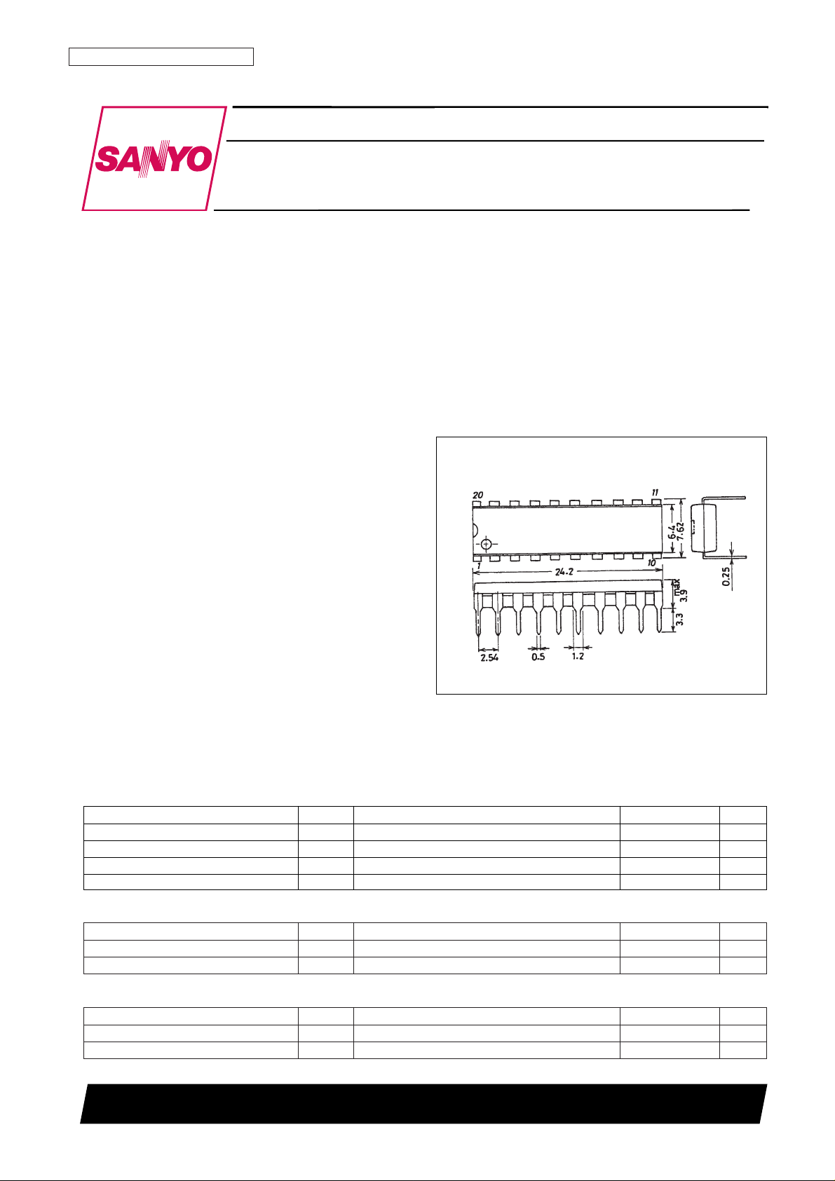
Package Dimension
unit: mm
3021B-DIP20
SANYO: DIP20
[LA2650]
LA2650
SANYO Electric Co.,Ltd. Semiconductor Bussiness Headquarters
TOKYO OFFICE Tokyo Bldg., 1-10, 1 Chome, Ueno, Taito-ku, TOKYO, 110 JAPAN
Bass Boost IC
Monolithic Linear IC
Parameter Symbol Conditions Ratings Unit
Maximum supply voltage V
CC
max 12 V
Allowable power dissipation Pd max Ta ≤ 70°C 450 mW
Operating temperature Topr –25 to +70 °C
Storage temperature Tstg –40 to +150 °C
Specifications
Maximum Ratings at Ta = 25°C
Parameter Symbol Conditions Ratings Unit
Recommended supply voltage V
CC
9V
Operating voltage range V
CC
op 5 to 10 V
Operating Conditions at Ta = 25°C
Parameter Symbol Conditions Ratings Unit
Low-level voltage V
IL
0 to 1.5 V
High-level voltage V
IH
3.5 to *5.5 V
Control Data Input Voltage Levels
Note: When VCCis under 5.7 V, the maximum value shall be VCC– 0.2 V.
Page 2

No. 5652-2/13
LA2650
Parameter Symbol Conditions
Ratings
Unit
min typ max
Quiescent current
I
CCO
T Boost: off 5 8 13 mA
I
CCO
B Boost: on 6 9 14 mA
Voltage gain
VGT V
IN
= 0 dBm, Boost: off –2 0 +2 dB
VGB V
IN
= 0 dBm, Boost: on –2 0 +2 dB
BST1
Boost: on, f
i
= 50 Hz, BST = 35 dB,
25.5 28.5 31.5 dB
ADD = 0 dB, V
IN
= –30 dBm
BST2
Boost: on, f
i
= 50 Hz, BST = 35 dB,
21 24 27 dB
Boost level: high
ADD = 0 dB, V
IN
= –20 dBm
BST3
Boost: on, f
i
= 50 Hz, BST = 35 dB,
13 15 17 dB
ADD = 0 dB, V
IN
= –10 dBm
BST4
Boost: on, f
i
= 50 Hz, BST = 35 dB,
5 7 9 dB
ADD = 0 dB, V
IN
= 0 dBm
BST1
Boost: on, f
i
= 50 Hz, BST = 30 dB,
15 18 21 dB
ADD = –6 dB, V
IN
= –20 dBm
Boost level: low
BST2
Boost: on, f
i
= 50 Hz, BST = 30 dB,
8 10 12 dB
ADD = –6 dB, V
IN
= –10 dBm
BST3
Boost: on, f
i
= 50 Hz, BST = 30 dB,
1.5 3.5 5.5 dB
ADD = –6 dB, V
IN
= 0 dBm
Maximum output voltage
V
O
maxT THD = 1%, Boost: off 2.00 2.55 V
V
O
maxB THD = 1%, Boost: on 2.00 2.55 V
THD T
V
IN
= –10 dBm, Boost: off,
0.008 0.03 %
Total harmonic distortion
BPF = 400 Hz to 30 kHz
THD B
VIN= –10 dBm, Boost: on, fi= 50 Hz,
0.3 0.9 %
LPF = 30 kHz
CT T
VO= 0 dB, Rg = 10 kΩ, DIN AUDIO,
80 88 dB
Crosstalk
Boost: off
CT B
VO= 0 dB, Rg = 10 kΩ, DIN AUDIO,
50 59 dB
Boost: on
V
NO
T
Rg = 10 kΩ, JIS A, Boost: off,
–97 –90 dBm
Output noise voltage
Boost ADD = off
V
NO
B Rg = 10 kΩ, JIS A, Boost: on –91 –84 dBm
LED current I
LED
RED LED 11 15 19 mA
Electrical Characteristics at Ta = 25°C, VCC= 9 V, fi= 1 kHz, RL= 10 kΩ, BST = 35 dB, ADD = 0 dB, BST:ADD = ON
Page 3
No. 5652-3/13
LA2650
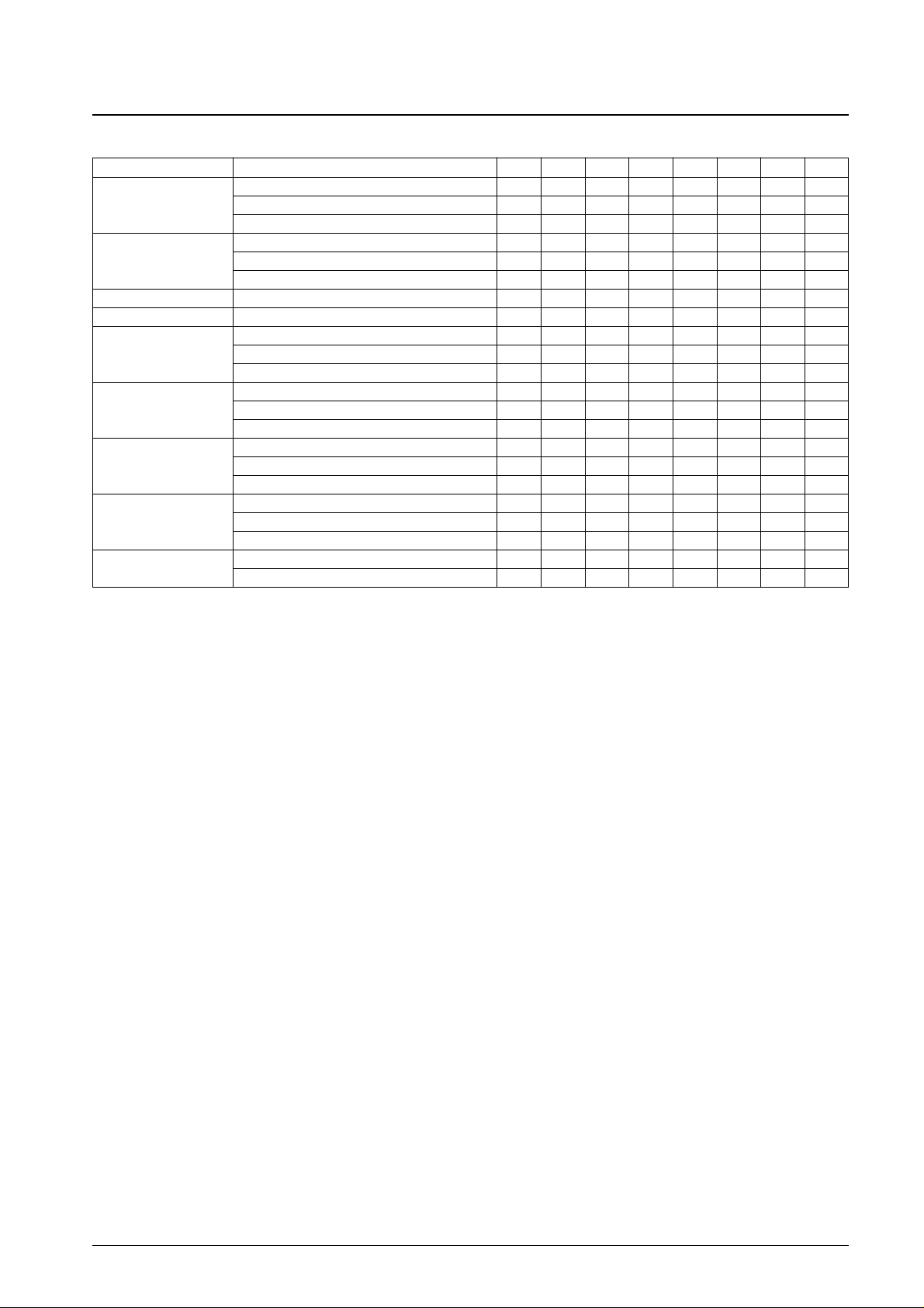
Control Data for the Parameters in the Electrical Characteristics
*=don’t care
Parameter Conditions D1 D2 D3 D4 D5 D6 D7 D8
Quiescent current
I
CCO
T Boost: on L L L L L L L L
I
CCO
B Boost: off H H H H H H L H
Voltage gain V
IN
= 0 dBm
VG T Boost: off L L L L L L L L
VG B Boost: on H H H H H H L H
Boost level: high Boost: on, f
i
= 50 Hz, BST = 35 dB, ADD = 0 dB H H H H H H L H
Boost level: low Boost: on, f
i
= 50 Hz, BST = 30 dB, ADD = –6 dB H L H L H H L H
Maximum output voltage THD = 1%
V
O
maxT Boost: off L L L L L L L L
V
O
maxB Boost: on H H H H H H L H
Total harmonic distortion V
IN
= –10 dBm
THD T Boost: off, BPF = 400 Hz to 30 kHz L L L L L L L L
THD B Boost: on, f
i
= 50 Hz, LPF = 30 kHz H H H H H H L H
Crosstalk V
O
= 0 dBm, Rg = 10 kΩ, DIN AUDIO
CT T Boost: off L L L L L L L L
CT B Boost: on H H H H H H L H
Output noise voltage Rg = 10 kΩ, JIS A
V
NO
T Boost: off, Boost ADD = off L L L L L L L L
V
NO
B Boost: on H H H H H H L H
LED current
I
LED
RED LED * * * * * * H *
Page 4
DC-CUT
VCA NF
5 to 10 V
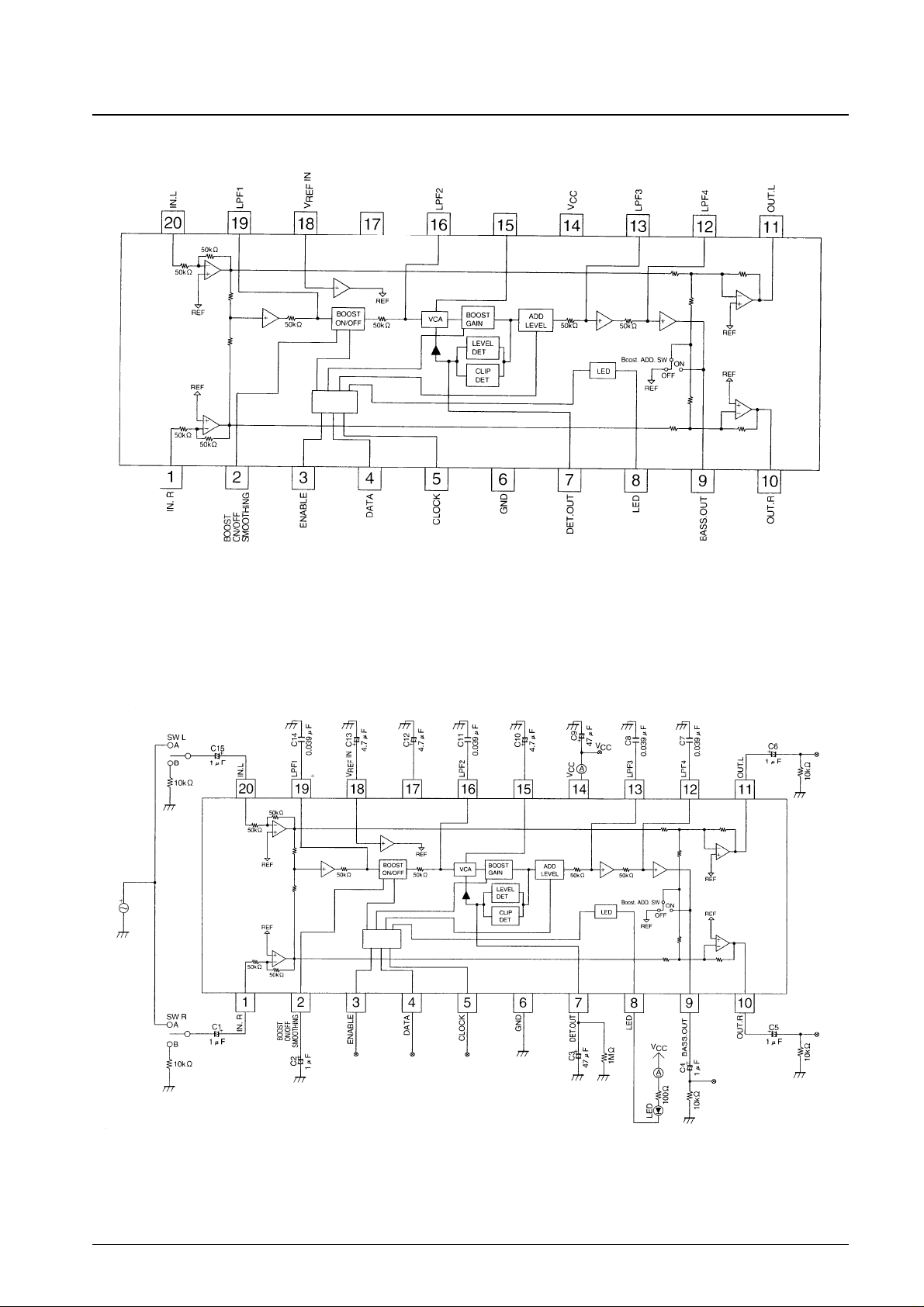
Block Diagram
No. 5652-4/13
LA2650
VCA NF
DC-CUT
DECODER
DECODER
Test Circuit
Page 5
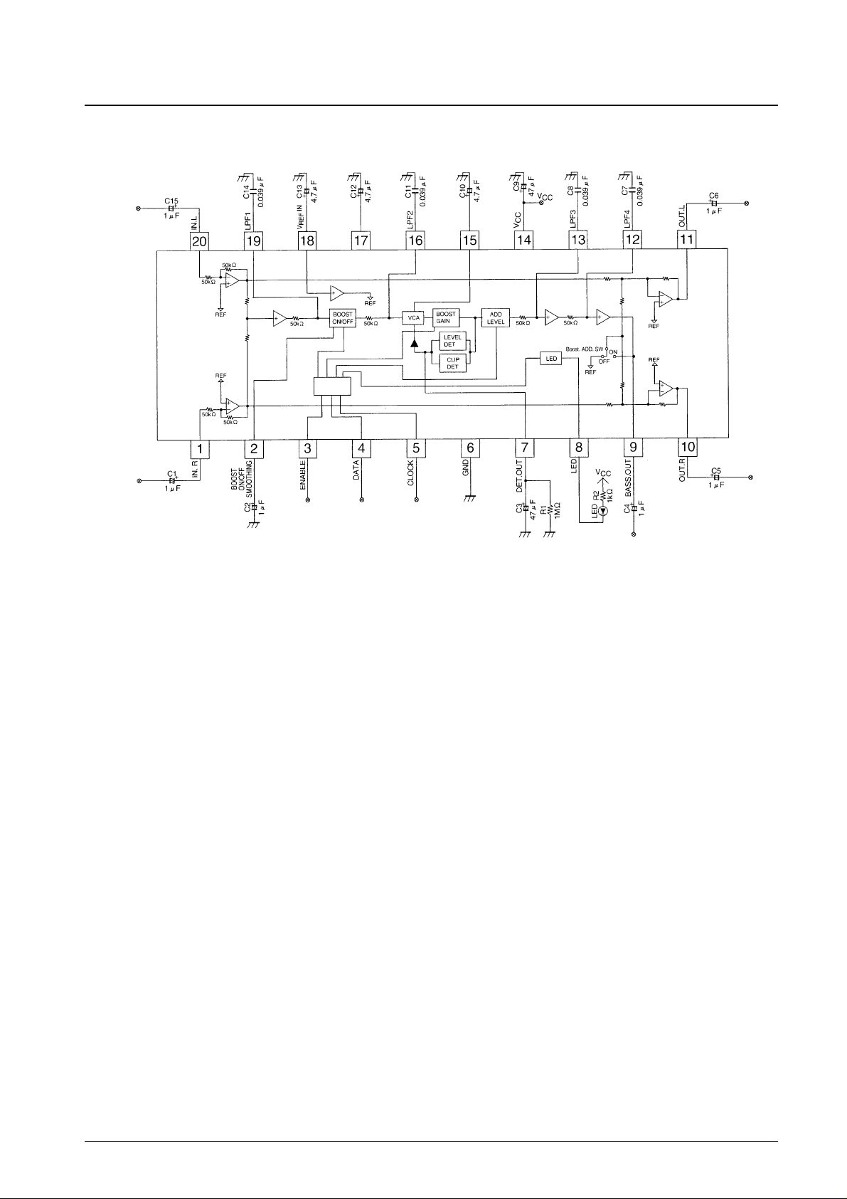
Sample Application Circuit
No. 5652-5/13
LA2650
DC-CUT
VCA NF
5 to 10 V
DECODER
Page 6
Notes on LA2650 Operation
LPF cutoff frequency
Use the following formula to calculate the cutoff frequency:
· fc = 1/(2πCR) Hz
However: R = 50 kΩ, since the resistor is on chip.
Thus the cutoff frequency can be set by the external capacitor.
Example: C = 0.039 µF (As in the sample application circuit)
fc = 81.6 Hz
Maximum boost gain
Use the following formula to calculate the maximum boost gain.
· BASS OUT total gain (GB) = α +4 × 20 log10(1 + 4π2f2C2R2)
–1/2
+ β
Here,
α = Boost gain (20, 25, 30, or 35 dB)
β = Addition level (0, –3, –6, –9, –15, –20, –25, or –35 dB)
f: Frequency
C: The LPF external capacitor
R = 50 kΩ (built in)
Example: When α = 35 dB, β = 0 dB, f = 50 Hz, C = 0.039 µF (As in the application circuit)
GB= 29.46 dB
No. 5652-6/13
LA2650
Pin Functions
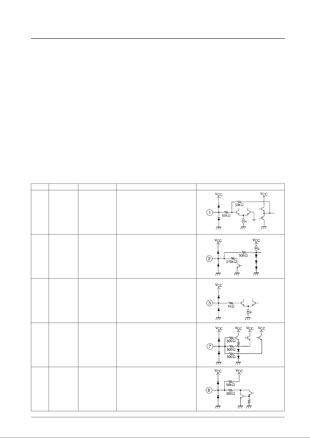
Pin No. Pin Pin voltage (V) Pin function Equivalent circuit
1 IN-L 1/2 V
CC
Signal input pin
20 IN-R The input impedance is 50 kΩ
2 BOOST 0.7 to 2 Smoothing pin for boost on/off switching
ON/OFF
SMOOTHING
3 ENABLE Apply either 0 or 5 V. Serial control data input pins
4 DATA
5 CLOCK
7 DET-OUT 1.7 to 3.5 The detection attack and recovery times are set
by the external resistor and capacitor connected
to this pin.
8 LED V
CC
max. LED cathode
Influx current: 20 mA (maximum)
Continued on next page.
Page 7

No. 5652-7/13
LA2650
Pin No. Pin Pin voltage (V) Pin function Equivalent circuit
9 BASS-OUT 1/2 V
CC
Low boost output for 3D systems
10 OUT-R 1/2 V
CC
Signal outputs
11 OUT-L
12 LPF4 1/2 V
CC
LPF connection for the low-boost circuit
13 LPF3 Internal resistor: 50 kΩ
19 LPF1
15 VCA NF 1/2 V
CC
VCA feedback
16 LPF2 1/2 V
CC
LPF connection for the low-boost circuit
Internal resistor: 50 kΩ
17 DC-CUT 1/2 V
CC
Connection for DC-cut capacitor
18 V
REF
IN 1/2 V
CC
V
REF
amplifier reference
Continued from preceding page.
Note: Pin voltage values are typical values.
Page 8

External Components
• C1, C15(0.22 to 10 µF)
Input coupling capacitor.
Note that the low-frequency gain is reduced at lower capacitances.
The value of these capacitors determines the extreme low-frequency cutoff.
• C2(0.22 to 2.2 µF)
Boost on/of switching circuit smoothing capacitor.
The on/off switching time can be adjusted by changing the value of this capacitor. However, note that if the value is
lowered excessively, switching noise (spikes) may appear.
• C3(10 to 220 µF)
Detection capacitor.
The attack and recover times can be adjusted by changing the value of this capacitor.
• C4, C5, C6(0.22 to 10 µF)
Output coupling capacitors.
• C7, C8, C11, C
14
Low boost LPF capacitors.
The low boost curve can be adjusted by changing the values of these capacitors. These capacitors may be omitted or,
inversely, secondary or tertiary structures may be used.
• C9(22 to 220 µF)
Power supply capacitor.
• C10(1.0 to 22 µF)
VCA NF capacitor.
Note that lowering the value of this capacitor will lower the low-frequency boost.
This capacitor determines the extreme low-frequency cutoff.
• C12(1.0 to 22 µF)
DC cut capacitor
Note that lowering the value of this capacitor will lower the low-frequency boost.
This capacitor determines the extreme low-frequency cutoff.
• C13(1.0 to 22 µF)
RF reference LPF capacitor.
The RF SVRR can be modified by changing the value of this capacitor.
• R1(200 kΩ to 3.9 MΩ)
Detection recovery time adjustment (discharge resistor)
Note that the total harmonic distortion is increased as the value of this resistor is reduced.
• R2(0 to 1 kΩ)
LED current adjustment.
LED current ≈ (VCC– V
LED
– 0.9)/(R2+ 300)
The maximum LED current is 20 mA.
No. 5652-8/13
LA2650
Page 9

Control Format
No. 5652-9/13
LA2650
Add Level Select
D1, D2, D3 Add level Notes
H, H, H 0 dB
H, H, L –3 dB
H, L, H –6 dB
H, L, L –9 dB
L, H, H –15 dB
L, H, L –20 dB
L, L, H –25 dB
L, L, L –35 dB Initial setting for the V
CC
on time
Boost Gain Select
D4, D5 Boost gain Notes
H, H 35 dB
H, L 30 dB
L, H 25 dB
L, L 20 dB Initial setting for the V
CC
on time
Left and right channel boost add on/off
L H
D6 off on
LED on/off
L H
D7 off on
Boost on/off
Mode Switching
• Add level select
— Selects the addition level at the output mixing amplifier for the low-frequency signals from the boost amplifier.
• Boost gain select
— Selects the amplification applied to low-frequency signals by the boost amplifier.
• Left and right channel boost add on/off
— Turns addition of the low-frequency boosted signal to the left and right channels on or off.
• LED on/off
— Turns the LED on or off.
• Boost on/off
— Turns the amplification of low-frequency signals on or off.
L H
D8 off on
Note: The VCCon time and all other data is initialized to low.
Data
Page 10
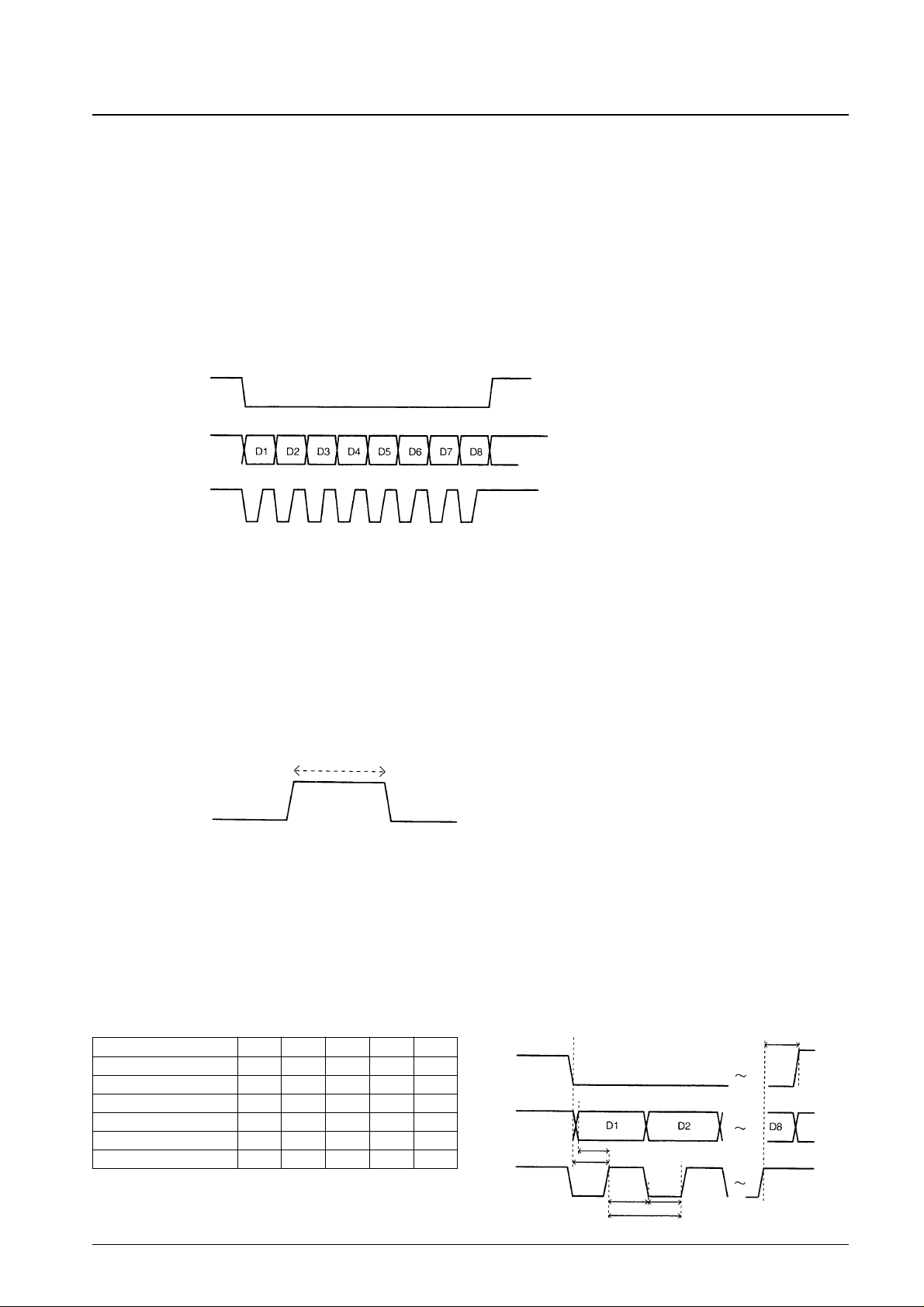
Recommended Data Transfer Procedure
The boost gain select and the left and right channel boost add on/off settings should only be set at power on. During
normal operation, control the device by setting the add level select and boost on/off settings. Using the add level select
and boost on/off settings for control is superior from the standpoint of minimizing switching noise (spikes).
Limiter (ALC) Operation
• The level limiter operates when the boost gain amplifier output level reaches about 2 V rms, and suppress further level
increases above that point.
• The non-clipping limiter operates to prevent boost gain amplifier output clipping at power-supply voltages (about 8.5 V
and lower) at which the output cannot be amplified to the operating level of the level limiter.
• Notes on Control Data
— Data is read in on the rising edge of the clock signal.
— Data consists of 8 bits, D1 through D8.
— The input data is latched on the rising edge of the enable signal.
— When the LA2650 is not being controlled, the clock and the enable signal must be held high.
— Intervals between commands
The timing of the intervals on the enable signal must meet the conditions shown in the figure below.
• Initial Settings at Power on
— All data is reset to low when power is first applied.
— Applications should send their initial data settings once the IC is fully operational after power is applied, i.e. about
0.5 second after power is applied.
• Data Timing
No. 5652-10/13
LA2650
Timing characteristics min typ max unit
Enable clock delay time t
ec
5 µs
Data clock delay time t
dc
5 µs
Clock high-level hold time t
ch
5 µs
Clock low-level hold time t
cl
5 µs
Clock enable delay time t
ce
5 µs
Clock cycle time t
ck
10 µs
At least 10 µs
Enable
Enable
Enable
t
ce
t
ch
t
ec
t
dc
t
ck
t
cl
Data
Data
Clock
Clock
Page 11
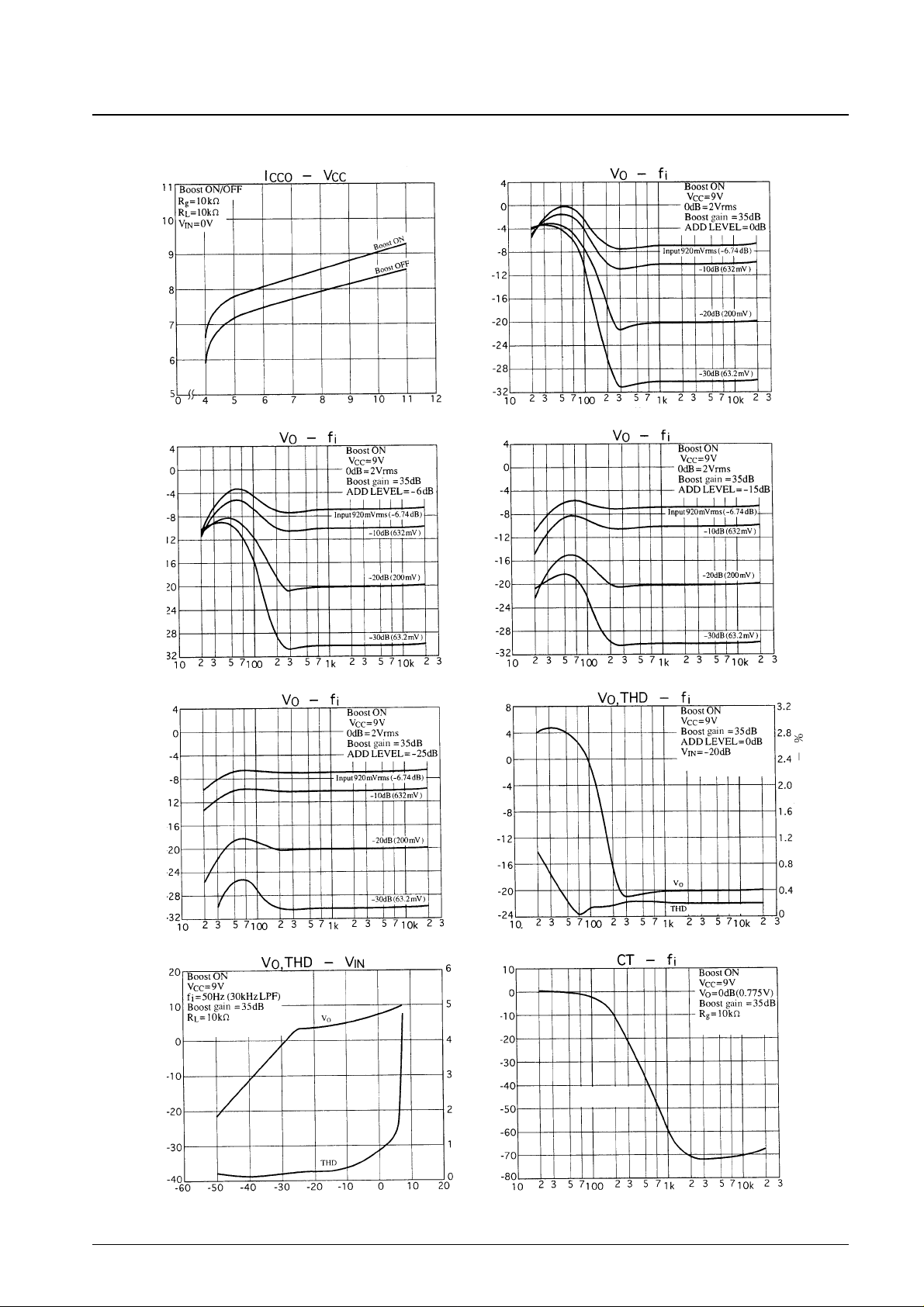
Total harmonic distortion, THD – %
crosstalk, CT – dB
No. 5652-11/13
LA2650
Quiescent current, I
CCO
– mA
Output voltage, V
O
– dB
Output voltage, V
O
– dB
Output voltage, V
O
– dB
Output voltage, V
O
– dB
Output voltage, V
O
– dBOutput voltage, V
O
– dB
Total harmonic distortion, THD – %
Supply voltage, VCC, – V
Input frequency, fi– Hz
Input frequency, fi– Hz
Input frequency, fi– Hz
Input voltage, VIN– dBm
Input frequency, fi– Hz
Input frequency, fi– Hz
Input frequency, fi– Hz
Filter: flat
Filter: 80 kHz LPF
L → R
R → L is identical.
I/O C = 1 µF
Page 12
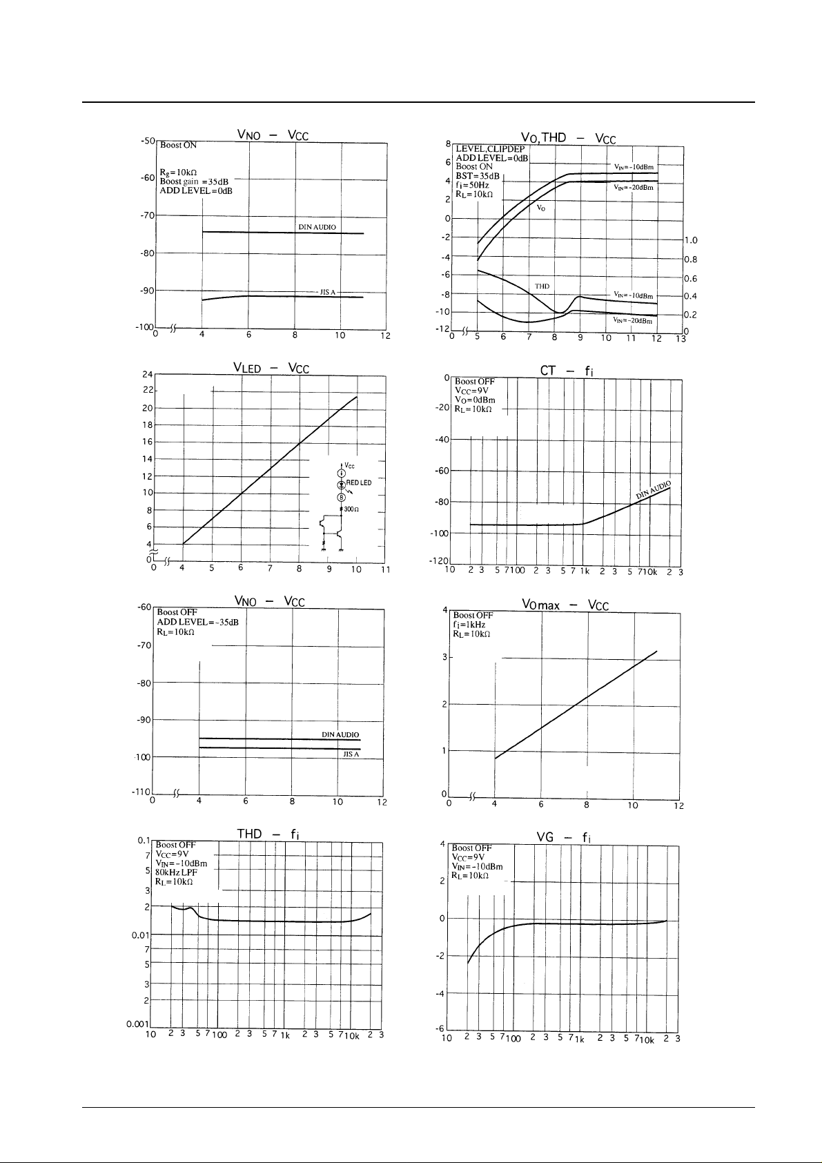
No. 5652-12/13
LA2650
Voltage gain, VG – dB
Output noise voltage, V
NO
– dB
Output voltage, V
O
– dBm
Current drain, I
LED
– mA
Output noise voltage, V
NO
– dBm
Total harmonic distortion, THD – %
Crosstalk, CT – dB
Maximum output voltage, V
Omax
– V
Supply voltage, VCC– V
Supply voltage, VCC– V
Supply voltage, VCC– V
Supply voltage, VCC– V
Input frequency, fi– Hz
Input frequency, fi– Hz
Supply voltage, VCC– V
Input frequency, fi– Hz
Input C = 1 µF
Input C = 1 µF
I/O C = 1 µF
THD = 1%
I/O C = 1 µF
Rg = 10 kΩ
RL= 10 kΩ
I/O C = 1 µF
I/O C = 1 µF
Rg = 10 kΩ
L → R
R → L is identical.
Total harmonic distortion, THD – %
With no LED
series resistor
Page 13
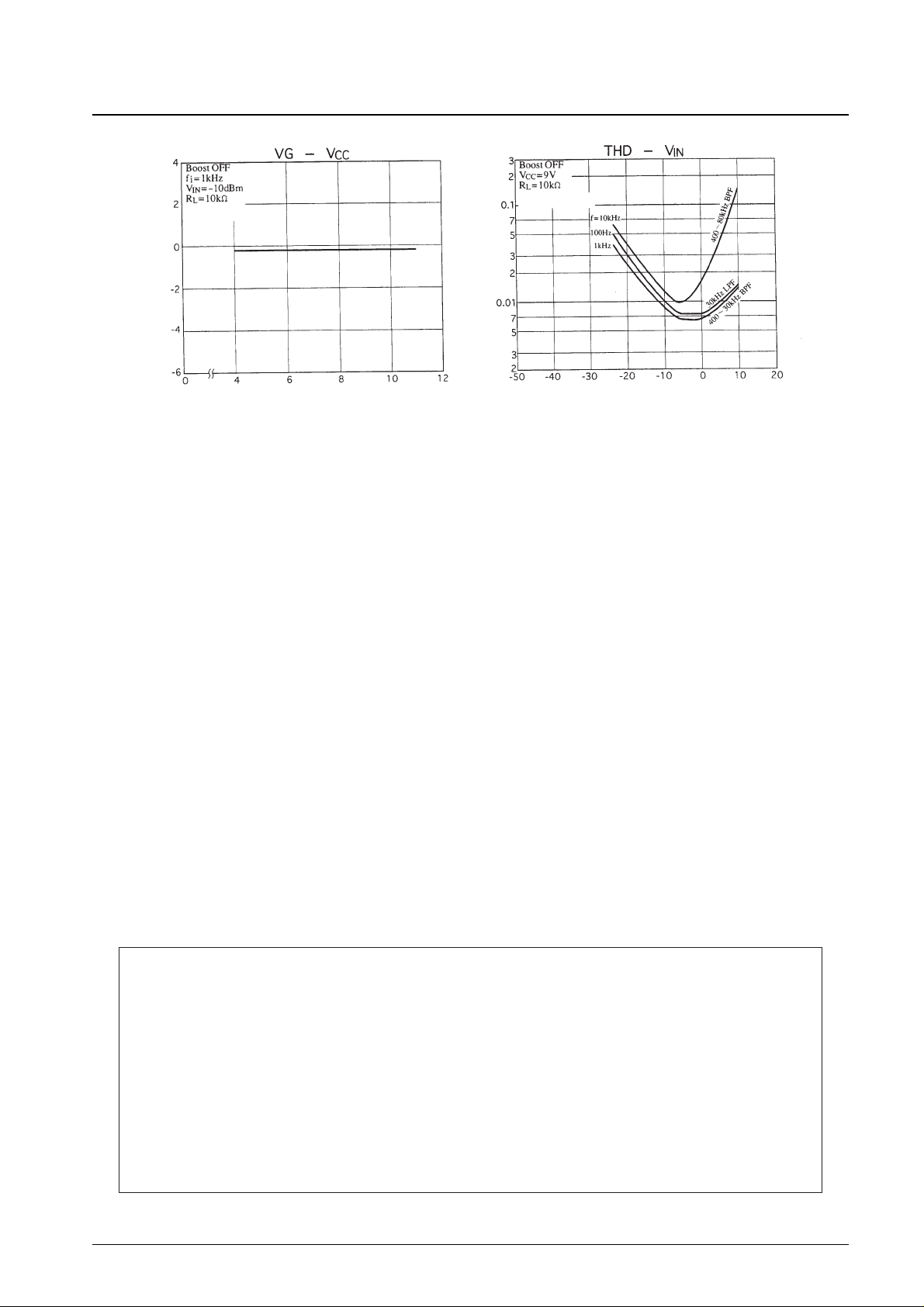
No. 5652-13/13
LA2650
This catalog provides information as of May, 1997. Specifications and information herein are subject to change
without notice.
■ No products described or contained herein are intended for use in surgical implants, life-support systems, aerospace
equipment, nuclear power control systems, vehicles, disaster/crime-prevention equipment and the like, the failure of
which may directly or indirectly cause injury, death or property loss.
■ Anyone purchasing any products described or contained herein for an above-mentioned use shall:
➀ Accept full responsibility and indemnify and defend SANYO ELECTRIC CO., LTD., its affiliates, subsidiaries and
distributors and all their officers and employees, jointly and severally, against any and all claims and litigation and all
damages, cost and expenses associated with such use:
➁ Not impose any responsibility for any fault or negligence which may be cited in any such claim or litigation on
SANYO ELECTRIC CO., LTD., its affiliates, subsidiaries and distributors or any of their officers and employees
jointly or severally.
■ Information (including circuit diagrams and circuit parameters) herein is for example only; it is not guaranteed for
volume production. SANYO believes information herein is accurate and reliable, but no guarantees are made or implied
regarding its use or any infringements of intellectual property rights or other rights of third parties.
Voltage gain, VG – dB
Supply voltage, VCC– V
Total harmonic distortion, THD – %
Input voltage, VIN– dBm
Input C = 1 µF
Input C = 1 µF
 Loading...