

Page 1

Overview
The LA2232 and LA2232M are RDS demodulator ICs
that provide both a 57 kHz bandpass filter as well as ARISK and DK signal recognition functions on chip. Costeffective RDS decoder systems can be constructed by
using an LA2232 or 2232M in conjunction with a
synchronization and error detection/correction LSI from
the LC7070 series. The LA2232 and 2232M provide
improved sensitivity LA2230 and 2230M.
Applications
• RDS signal demodulation
• ARI signal demodulation and SK and DK recognition
Functions
• 57 kHz bandpass filter
• RDS signal demodulation
• Bit rate clock regeneration
• RDS identification output
• ARI signal demodulation
• SK identification output
• DK identification output
• Adjustable ARI detection sensitivity
Features
• High RDS demodulation sensitivity
• Reduced costs and PCB area due to the inclusion of an
on-chip 57 kHz bandpass filter
• Supports improved interference rejection characteristics
by providing ARI detection sensitivity adjustment
• Quick operation startup due to a built-in rapid charging
circuit for use at power application.
Package Dimensions
unit: mm
3067-DIP24S
unit: mm
3112-MFP24S
Ordering number : EN4416A
21097HA(OT) No. 4416-1/9
SANYO: DIP24S
[LA2232]
SANYO: MFP24S
[LA2232M]
SANYO Electric Co.,Ltd. Semiconductor Bussiness Headquarters
TOKYO OFFICE Tokyo Bldg., 1-10, 1 Chome, Ueno, Taito-ku, TOKYO, 110 JAPAN
RDS Decorder
LA2232, 2232M
Monolithic Linear IC
Page 2

No. 4416A-2/9
LA2232, 2232M
Specifications
Maximum Ratings at Ta = 25°C
Parameter Symbol Conditions Ratings Unit
Maximum supply voltage V
CC
max Pins 13, 14, 15, 23 12 V
LA2232: Ta ≤ 80°C 450 mW
Allowable power dissipation Pd max LA2232M: Ta ≤ 37.5°C 450 mW
LA2232M: Ta = 80°C 280 mW
Entering current I
LED
Pins 13, 14, 15 20 mA
Operating temperature Topr –30 to +80 °C
Storage temperature Tstg
LA2232 –40 to +125 °C
LA2232M –40 to +150 °C
Operating Conditions at Ta = 25°C
Parameter Symbol Conditions Ratings Unit
Recommended supply voltage V
CC
Pin 23 5.0 V
Operating voltage range V
CC
op Pin 23 4.7 to 5.5 V
Operating Characteristics at Ta = 25°C, VCC= 5.0 V
Ratings
Parameter Symbol
min typ max
Unit
Quiescent current 14 22 28 mA
Band pass filter gain f = 57 kHz 9 12.5 17 dB
f = 60 kHz (57 kHz = 0 dB) –6 –2.5 0 dB
Band pass filter selectivity f = 54 kHz (57 kHz = 0 dB) –6 –3.5 0 dB
f = 38 kHz (57 kHz = 0 dB) –39 –33 dB
PLL capture range 5 mVrms CW input
–0.5 %
+0.8 %
RDS detection sensitivity The pin 6 input when pin 15 goes low 0.4 1.0 mVrms
SK detection sensitivity The pin 6 input when pin 14 goes low 1.0 2.0 mVrms
DK detection sensitivity The pin 6 input when pin 13 goes low 1.1 2.0 mVrms
The maximum input on pin 6 for the (ARI + RDS)
30 50 mVrms
RDS
signal when pin 15 goes low
Input dynamic range
The maximum input on pin 6 for the RDS signal
250 mVrms
when pin 15 goes low
DK
The maximum input on pin 6 for the ARI signal
75 100 mVrms
when pin 15 goes low
Bit rate clock jitter ±8 ±9 ±10 µs
RDS lockup time
The time until pin 15 goes low following RDS
35 ms
becoming a 3 mV input
SK lockup time
The time until pin 14 goes low following ARI 45 ms
becoming an 8 mV input
SK + RDS lockup time
The time until pin 15 goes low following RDS +
80 ms
ARI becoming an 8.5 mV input
Data output
The high level for pin 17 4.7 4.9 5.0 V
The low level for pin 17 0 0.1 0.3 V
Bit rate clock output
The high level for pin 18 4.7 4.9 5.0 V
The low level for pin 18 0 0.1 0.3 V
VCO free-running frequency 453 456 459 kHz
Page 3
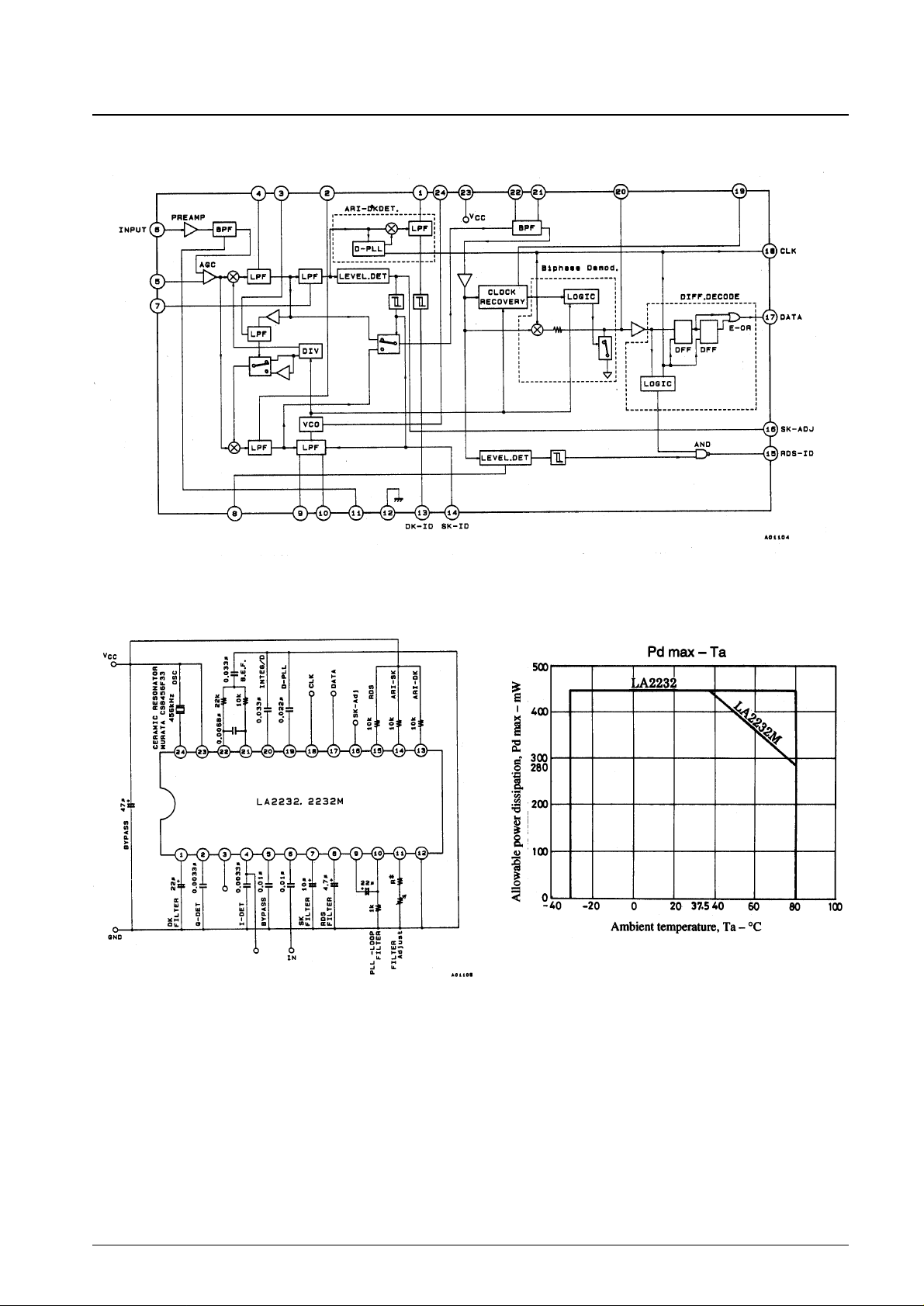
Equivalent Circuit Block Diagram
Test Circuit
No. 4416A-3/9
LA2232, 2232M
*R = 6.8 kΩ (for the LA2232)
R = 5.6 kΩ (for the LA2232M
Unit (resistance: Ω, capacitance: F)
Page 4
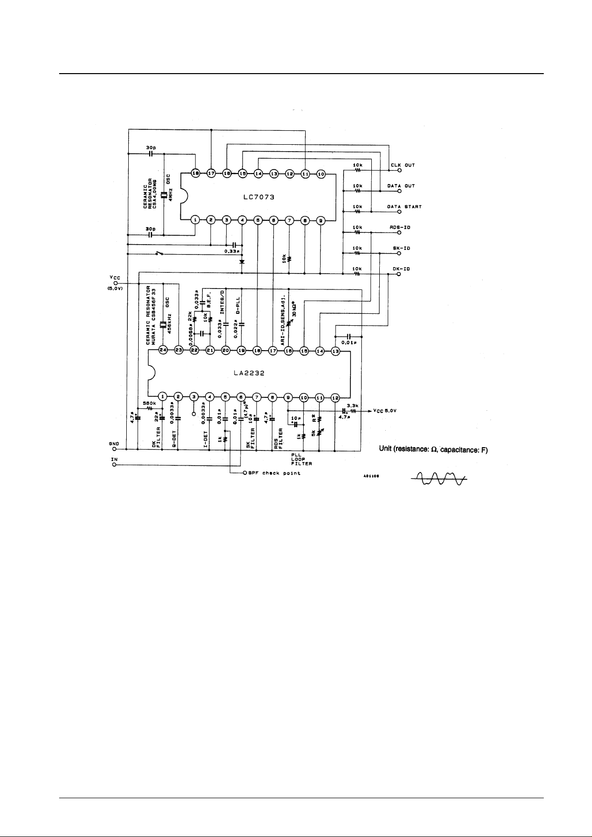
Sample Application Circuit Using the LA2232/M and the LC7073/M
Adjusting the 57 kHz BPF
(A) Check the output level of the bi-phase signal from pin 4 or pin 22 (with the pin 6 RDS input at about 1 mVrms and the ALC circuit not operating).
(B) Check the signal level of the BPF checkpoint (with the pin 6 RDS input in the range 3 to 6 mVrms or higher).
No. 4416A-4/9
LA2232, 2232M
3 to 6 mVrms
Recommended input signal level
(when RDS ∆f = ±2.0 kHz)
*R = 6.8 kΩ (for the LA2232)
R = 5.6 kΩ (for the LA2232M)
↑
Bi-phase signal
Page 5
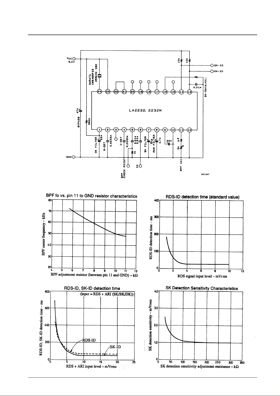
ARI Decoder Application Circuit
No. 4416A-5/9
LA2232, 2232M
*R = 6.8 kΩ (for the LA2232)
R = 5.6 kΩ (for the LA2232M)
Unit (resistance: Ω, capacitance: F)
Page 6
No. 4416A-6/9
LA2232, 2232M
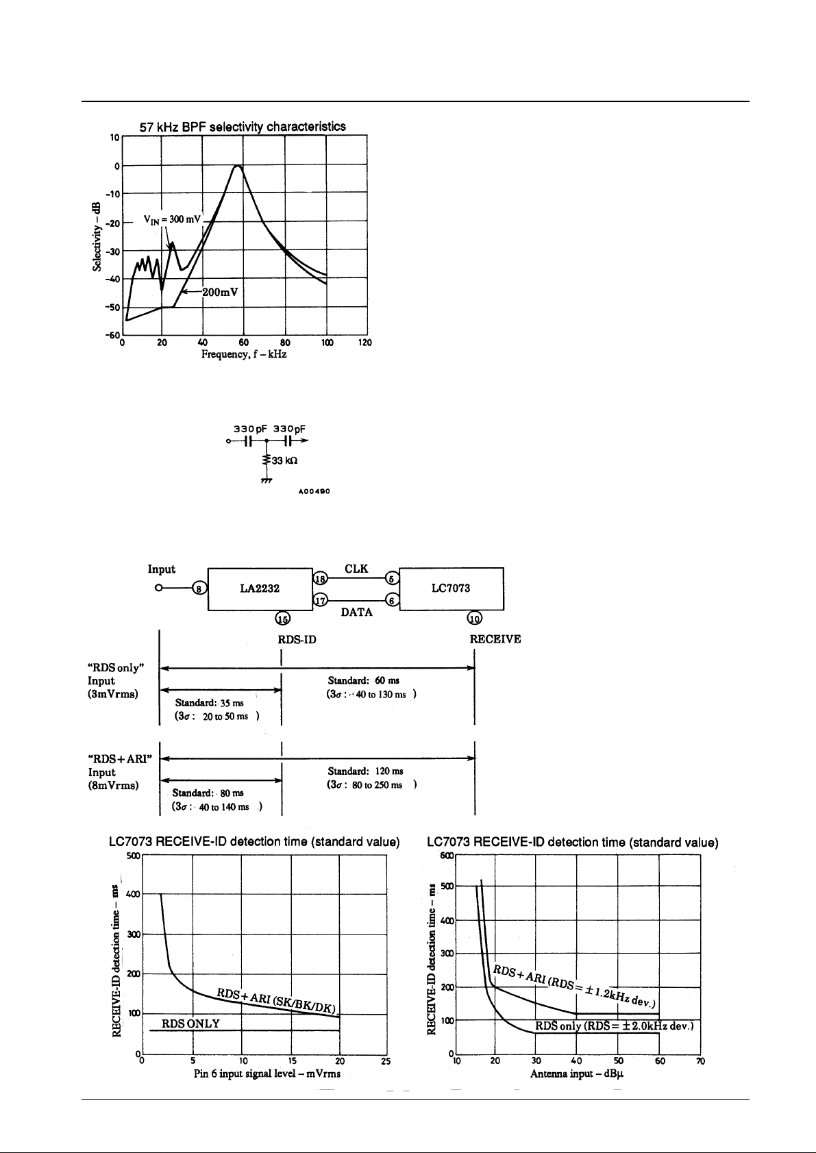
• For the LA2232, an input level of under 300 mVrms on pin 6 is desirable for a 100% FM demodulation output.
• We recommend the use of a pre-high pass filter as shown in the figure below if the 100% FM demodulation output level is over 300 mVrms.
FM demodulation signal input To the LA2232 pin 6
RDS-ID (LA2232), RECEIVE-ID (LC7073) Detection Time
(the RECEIVE-ID indicates synchronization completion).
Page 7
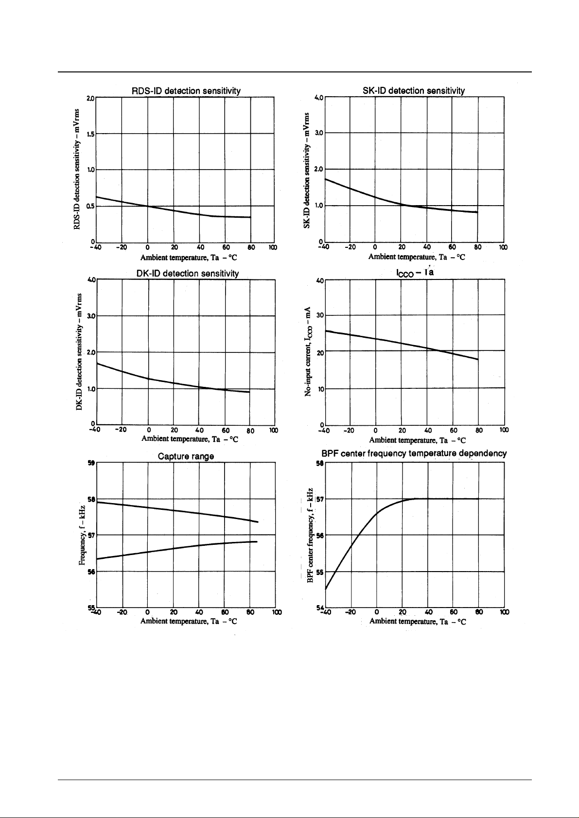
No. 4416A-7/9
LA2232, 2232M
Page 8
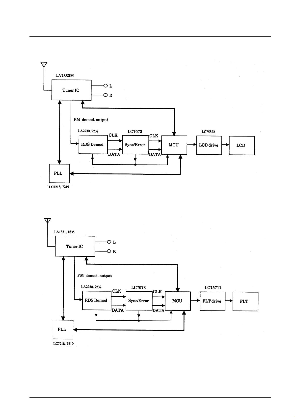
RDS Application IC Lineup
(1)
(2)
No. 4416A-8/9
LA2232, 2232M
Page 9

No. 4416A-9/9
LA2232, 2232M
This catalog provides information as of July, 1997. Specifications and information herein are subject to change
without notice.
■ No products described or contained herein are intended for use in surgical implants, life-support systems, aerospace
equipment, nuclear power control systems, vehicles, disaster/crime-prevention equipment and the like, the failure of
which may directly or indirectly cause injury, death or property loss.
■ Anyone purchasing any products described or contained herein for an above-mentioned use shall:
➀ Accept full responsibility and indemnify and defend SANYO ELECTRIC CO., LTD., its affiliates, subsidiaries and
distributors and all their officers and employees, jointly and severally, against any and all claims and litigation and all
damages, cost and expenses associated with such use:
➁ Not impose any responsibility for any fault or negligence which may be cited in any such claim or litigation on
SANYO ELECTRIC CO., LTD., its affiliates, subsidiaries and distributors or any of their officers and employees
jointly or severally.
■ Information (including circuit diagrams and circuit parameters) herein is for example only; it is not guaranteed for
volume production. SANYO believes information herein is accurate and reliable, but no guarantees are made or implied
regarding its use or any infringements of intellectual property rights or other rights of third parties.
 Loading...