

Page 1

Ordering number: EN4158
Monolithic Linear IC
LA2000M
Audio Level Sensor
Overview
LA2000M is an IC for detecting interprogram spaces to pick
out the starting point of a program immediately preceding or
following a musical program recorded on tape, and to detect
end of tape.
Used in
.
Radio-cassette recorders
.
Cassette decks
.
Car stereos
Applications
.
Detection of spaces between programs recorded on tape
.
Detection of end of tape
.
Other
Features
.
Has transistors capable of driving plungers with maximum
50 mA, and a protective diode to prevent induced reverse
voltages.
.
Can provide designated time delays by externally connected
capacitors and resistors.
.
Has a comparator with stable hysteresis to handle variations
in power supply voltage.
.
Detects unrecorded portions of tape.
Package Dimensions
unit : mm
3032B-MFP8
[LA2000M]
SANYO : MFP8
Specifications
Maximum Ratings at Ta = 25°C
Parameter Symbol Conditions Ratings Unit
Maximum supply voltage V
Allowable power dissipation Pd max 300 mW
Flow-in current I
Operating temperature Topr −20 to +75 °C
Storage temperature Tstg −40 to +125 °C
Note:1. The voltage at pin 7 must not exceed the supply voltage at pin 8.
2. The maximum current flowing into pin 7 should be no greater than 0.5 mA.
max 15 V
CC
max 50 mA
6
SANYO Electric Co.,Ltd. Semiconductor Bussiness Headquarters
TOKYO OFFICE Tokyo Bldg., 1-10, 1 Chome, Ueno, Taito-ku, TOKYO, 110 JAPAN
42896HA(II) No. 4158-1/7
Page 2
LA2000M
Operating Conditions at Ta = 25°C
Parameter Symbol Conditions Ratings Unit
Operating supply voltage V
Operating Characteristics at Ta = 25°C, VCC=9.0V,f=1kHz
Parameter Symbol Conditions min typ max Unit
Circuit current I
Output transistor saturating
voltage
Output diode forward voltage V
Output-off level in input
equivalent
Comparator-on level V
Comparator-off level V
Pin 7 high level V
Output transistor leakage
current
Output diode leakage current I
CC
V
CE (sat)I6
V
TH-H
TH-L
7
I
L-TR
L-Di
op 3.5 to 14 V
CC
f = 1 kHz, VIN= −45 dBm 6 12 mA
= 50 mA 0.5 1.8 V
IF= 50 mA 0.7 1.5 V
F
IN
f = 1 kHz −43 −50 −54 dBm
pin 0.45 0.55 V
3.0 3.5 4.0 V
1.8 2.2 2.6 V
100 µA
100 µA
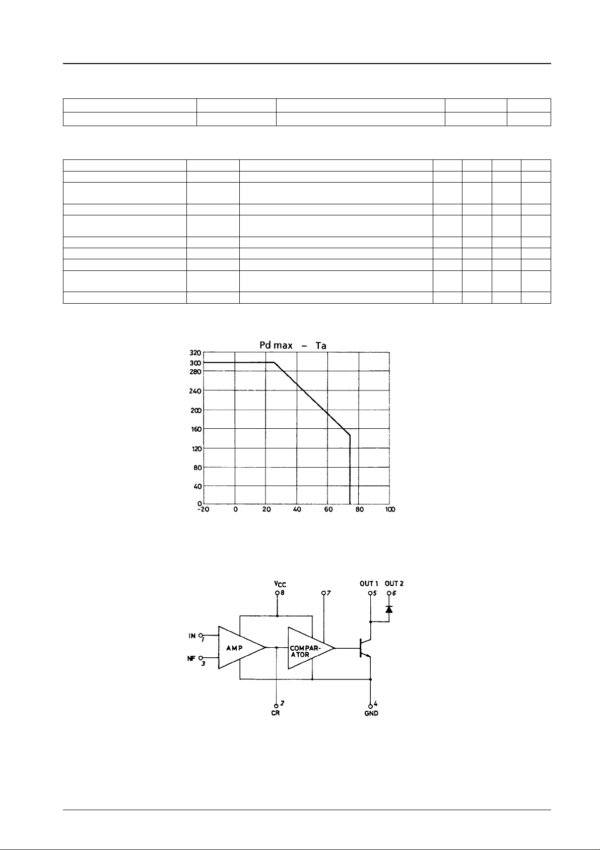
Allowable power dissipation, Pd max − mW
Equivalent Circuit Block Diagram
Ambient temperature, Ta − °C
No.4158-2/7
Page 3
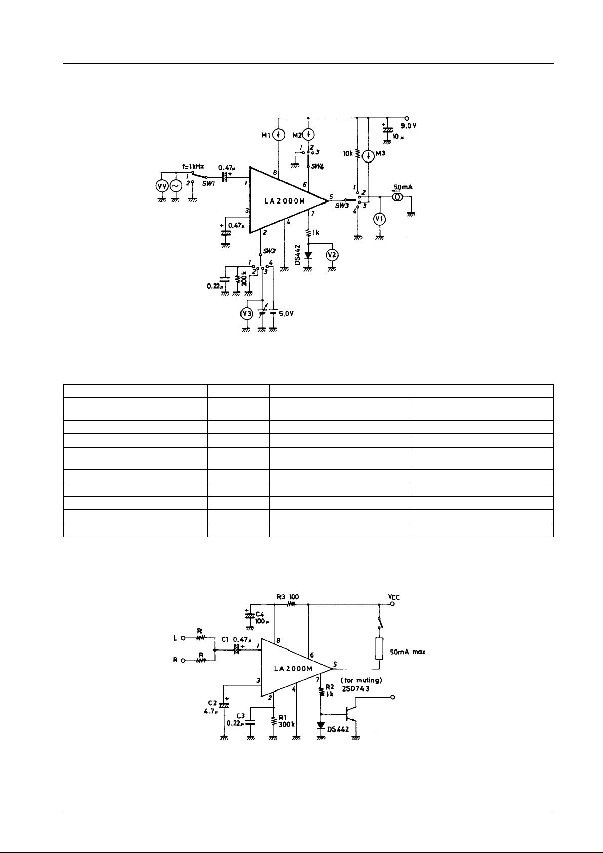
Test Circuit
LA2000M
Unit (resistance: Ω, capacitance: F)
Test Conditions
Test items Symbol SW-1 SW-2 SW-3 SW-4 Conditions
Circuit current I
Output transistor saturation voltage V
Output diode forward voltage V
Output-off level in input equivalent V
Comparator-on level V
Comparator-off level V
Pin 7 high level Vp-7 2413Measure V
Output transistor leakage current I
Output diode leakage current I
CC
CE (sat)
F
IN
H
L
TL
DL
1113Measure current flowing into pin 8 at
2223Measure VINat pin 5
2421Measure VINat pin 5
1113Input level (v.v) when pin 5 turns
2313Measure V3when pin 5 turns over
2313Measure V3when pin 5 turns over
2433Measure M3
2442Measure M2
V
IN
over
= −45 dB
Sample Application Circuit 1
Mechanism-coupled switch
(OFF at play mode)
Plunger
at pin 7
2
Unit (resistance: Ω, capacitance: F)
No.4158-3/7
Page 4
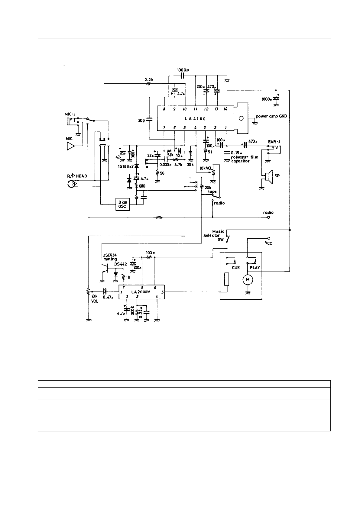
Sample Application Circuit 2
LA2000M
Use a mechanism for the plunger off while
functioning for program selection
Unit (resistance: Ω, capacitance: F)
1. Externally connected components
C1 Input coupling capacitor 0.47 to 2.2 µF recommended.
C2 NF capacitor Capacitance is reduced, so the off level in input equivalent becomes lower in the bass
C3, R1 For designation of time delays Any time delay can be obtained by adequate choice of C3 and R1. We recommend
C4, R3 Power supply ripple filter
R2 Bias resistor For diode when pin 7 is used to drive external transistors. A 1 kΩ resistor is
frequency range. We recommend 1 to 10 µF.
150 kΩ to 500 kΩ for R1.
recommended.
No.4158-4/7
Page 5
2. Individual pins and their operations
Input signal level, VIN− dBm
LA2000M
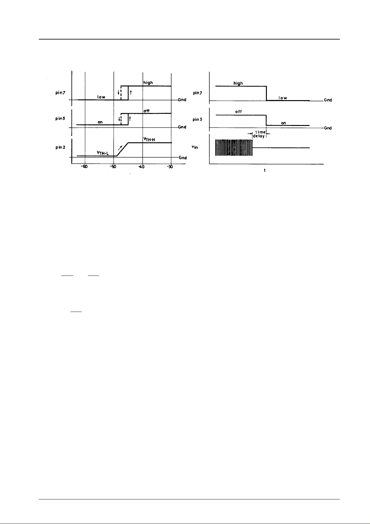
As shown above, when input level is raised and the pin 2 voltage reaches the V
over. (V
.
pin 5 is for driving plungers. When it is on the ‘‘L’’ side, pin 5 turns on and can draw current up to 50 mA maximum.
.
Pin 6 is a diode that prevents reverse voltages induced when the plunger is turned off from on.
.
Pin 7 functions in phase with pin 5 and can drive external transistors (such as for MUTE).
3. Time delays and obtaining CRs
When input signals that have been applied at a level not less than −45 dBm are removed, discharging occurs through the CR
connected at pin 2, lowering pin 2 potential. A time delay is provided before the hysteresis comparator turns over.
Accordingly,
E1/E0, within the IC, is 0.26. A desired time delay is obtained by an appropriate choice of τ (τ =C
is obtained by the following formula:
We recommend 150 kΩ to 500 kΩ for R when determining CR.
= −45 dBm).
IN
E1
E0
t=−τIn
t = 1.34 × C
E1
E0
=−
3R1
t
τ
e
(sec)
E0 : Initial voltage
E1 : Threshold voltage
τ : Time constant
level of the comparator, pins 5 and 7 turn
TH-H
). Therefore, the time delay
3R1
4. IC usage notes
.
Maximum ratings
When maximum ratings are surpassed, destruction or deterioration may result.
.
Interpin short circuits and reverse insertions
These cause destruction or deterioration of the IC: be careful when mounting on circuit board.
.
Voltage applied to pin 7 should never exceed pin 8 voltage.
.
The current flowing into pin 7 is to be 0.5 mA maximum.
No.4158-5/7
Page 6
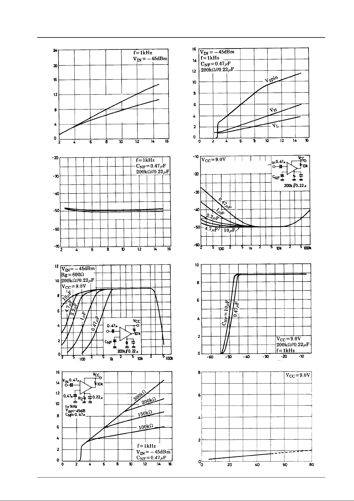
ICC−V
CC
LA2000M
pin, VH,VL−V
V
2
CC
−mA
CC
Circuit current, I
− dBm
IN
Input level, V
Quiescent
Operating
Supply voltage, VCC−V
VIN−V
CC
Off
On
−V
L
,V
H
pin, V
2
V
Input level when pin 5
[L] → [H]
− dBm
IN
Input level, V
Supply voltage, VCC−V
V
−f
IN
pin−V
2
V
pin−V
2
V
Supply voltage, V
V2pin−f
Frequency,f−Hz
V2pin−V
CC
CC
−V
pin−V
2
V
−V
CE (sat)
V
Frequency,f−Hz
pin−V
V
2
IN
Input level, VIN− dBm
V
CE (sat)−IC
Supply voltage, VCC−V
Output transistor saturation voltage,
Collector current, IC−mA
No.4158-6/7
Page 7
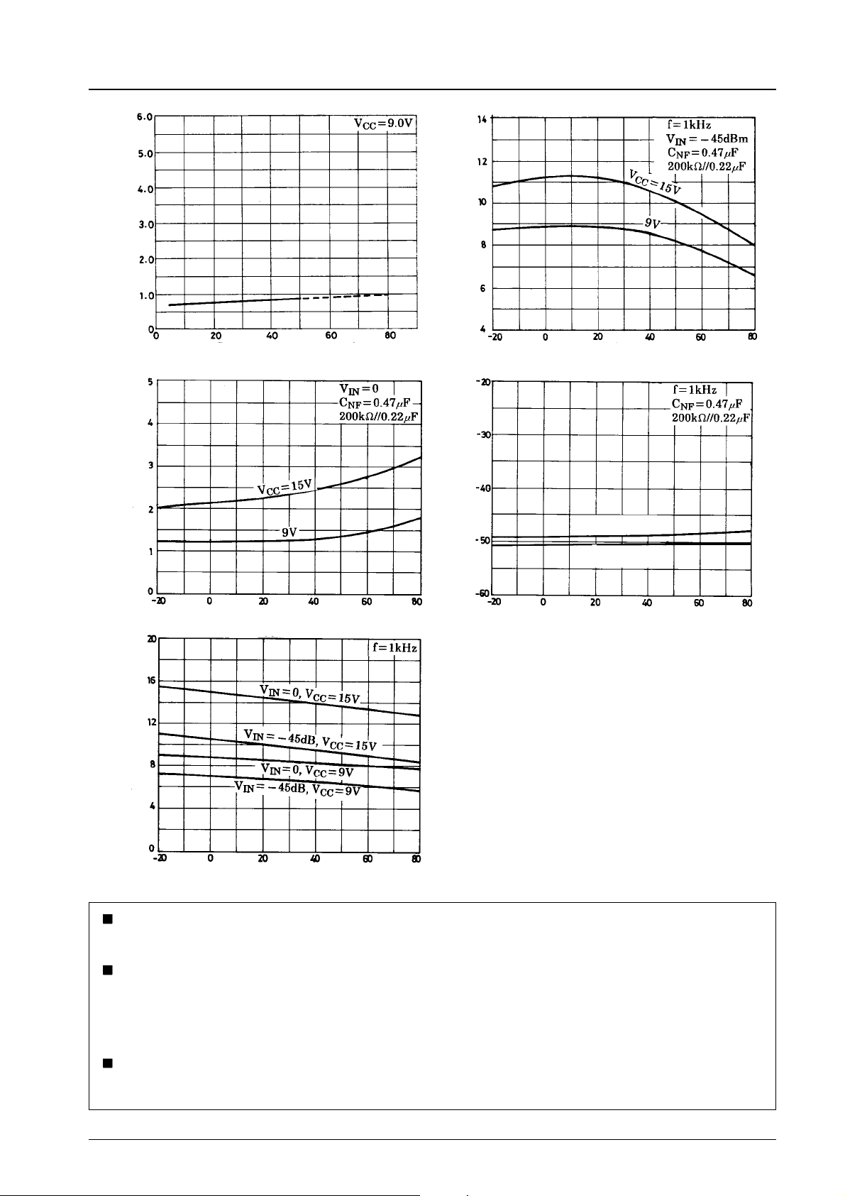
LA2000M
−V
F
Output diode forward voltage, V
pin−mW
2
V
VF−Di
Diode forward current, Di − mA
V2pin−Ta
pin−V
2
V
− dBm
IN
Input level, V
pin−Ta
V
2
Ambient temperature, Ta − °C
−Ta
V
IN
Off level
On level
Ambient termperature, Ta − °C
Ambient temperature, Ta − °C
ICC−Ta
−mA
CC
Circuit current, I
Ambient temperature, Ta − °C
No products described or contained herein are intended for useinsurgicalimplants, life-support systems, aerospace equipment,
nuclear power control systems, vehicles, disaster/crime-prevention equipment and the like, the failure of which may directly or
indirectly cause injury, death or property loss.
Anyone purchasing any products described or contained herein for an above-mentioned use shall:
1 Accept full responsibility and indemnify and defend SANYO ELECTRIC CO., LTD., its affiliates, subsidiaries and distributors
and all their officers and employees, jointly and severally, against any and all claims and litigation and all damages, cost and
expenses associated with such use:
2 Not impose any responsibility for any fault or negligence which may be cited in any such claim or litigation on SANYO
ELECTRIC CO., LTD., its affiliates, subsidiaries and distributors or any of their officers and employees jointly or severally.
Information (including circuit diagrams and circuit parameters) herein is for example only; it is not guaranteed for volume
production. SANYO believes information herein is accurate and reliable, but no guarantees are made or implied regarding its use
or any infringements of intellectual property rights or other rights of third parties.
This catalog provides information as of April, 1996. Specifications and information herein are subject to change without notice.
No.4158-7/7
 Loading...