

Page 1
Overview
The LA1837 is a single-chip AM/FM IF and MPX IC that
supports electronic tuning and was developed for use in
home stereo systems. It is optimal for use in automatic
station selection systems that use the SD and IF counting
techniques.
Functions
AM: RF amplifier, mixer, oscillator, IF amplifier,
detector AGC, oscillator buffer, S-meter, narrowband SD, IF buffer
FM IF: IF amplifier, quadrature detector, S-meter, S-
curve detector, IF buffer output
MPX: PLL stereo decoder, stereo display, forced mono,
VCO stop, post amplifier, audio muting, adjacent
channel interference rejection function
Features
• On-chip MPX VCO (no external components required)
• Adjacent channel interference rejection function
(third and fifth order)
• Supports both the SD and the IF counting techniques.
•
The AM and FM SD sensitivities can be set independently.
•
The AM and FM output levels can be set independently.
•
Improved AM practical sensitivity and high-input
distortion characteristics
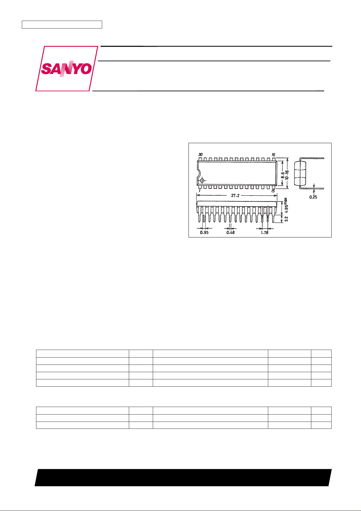
Package Dimensions
unit: mm
3061-DIP30S
Monolithic Linear IC
Ordering number : EN5688
82097HA(OT) No. 5688-1/9
SANYO: DIP30S
[LA1837]
SANYO Electric Co.,Ltd. Semiconductor Bussiness Headquarters
TOKYO OFFICE Tokyo Bldg., 1-10, 1 Chome, Ueno, Taito-ku, TOKYO, 110 JAPAN
Single-Chip Home Stereo IC with
Electronic Tuning Support
LA1837
Parameter Symbol Conditions Ratings Unit
Maximum supply voltage V
CC
max 12 V
Allowable power dissipation Pd max Ta ≤ 70°C 550 mW
Operating temperature Topr –20 to + 70 °C
Storage temperature Tstg –40 to +125 °C
Specifications
Maximum Ratings at Ta = 25°C
Parameter Symbol Conditions Ratings Unit
Recommended supply voltage V
CC
9V
Operating voltage range V
CC
op 7 to 11 V
Operating Conditions at Ta = 25°C
Page 2
No. 5688-2/9
LA1837
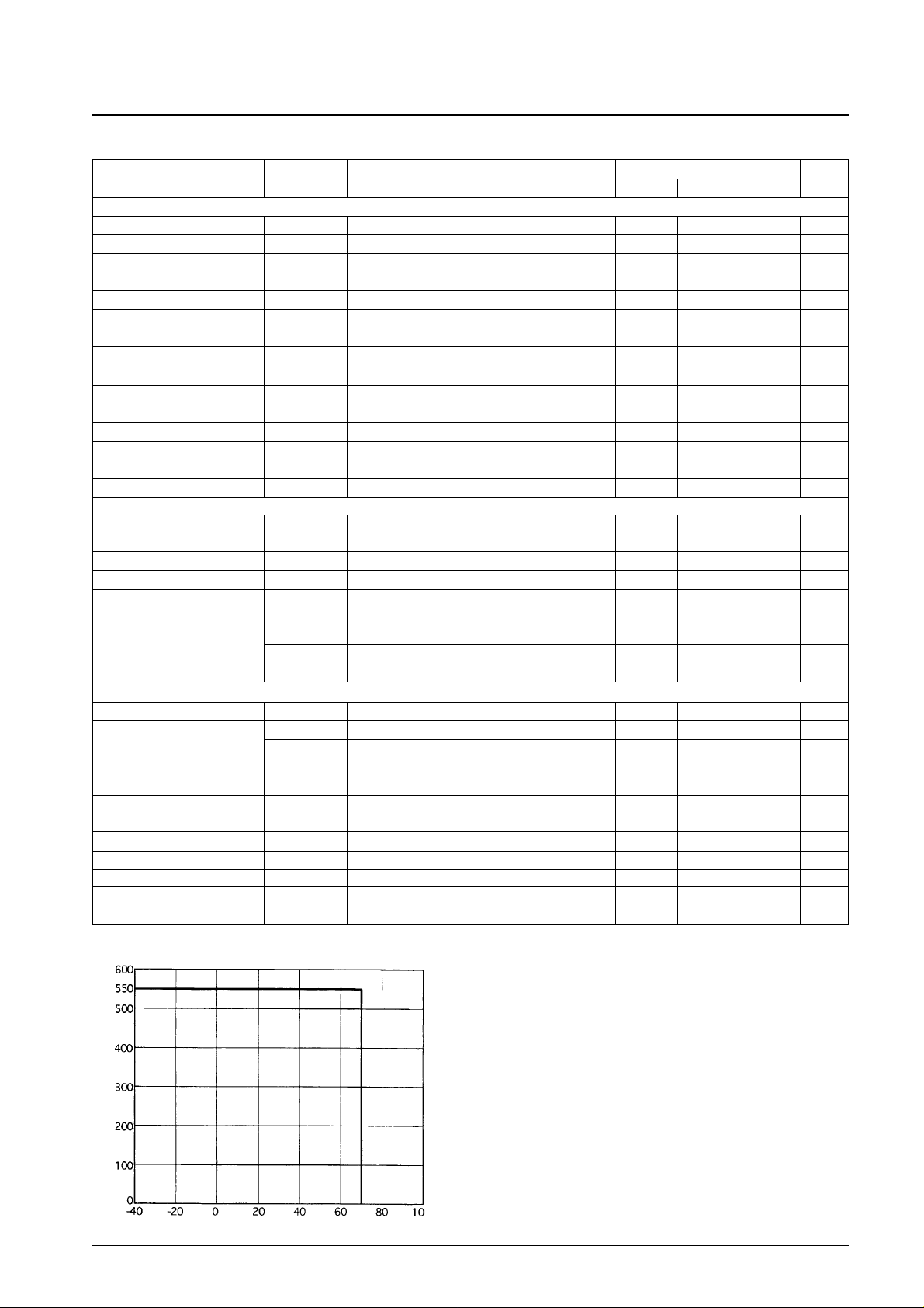
Parameter Symbol Conditions
Ratings
Unit
min typ max
[FM Mono Characteristics] fc = 10.7 MHz, fm = 1 kHz, with the coil adjusted so that V
AFC
– V
REG
= 0 V
Current drain I
CCO
-FM
With no input 18 31 44 mA
Demodulation output V
O
FM
100 dBµ, 100% mod. The pin 16 output 730 1100 1460 mVrms
Channel balance C.B-mono 100 dBµ, 100% mod. The pin 16 output/pin 17 output –1.5 0 +1.5 dB
Total harmonic distortion (mono) THD
FM(1)
100 dBµ, 100% mod. The pin 16 output 0.3 1.3 %
Total harmonic distortion (mono) THD
FM(2)
100 dBµ, 200% mod. The pin 16 output 1.0 5 %
Signal-to-noise ratio S/N
FM
100 dBµ, 100% mod. The pin 16 output 72 80 dB
AM rejection ratio AMR 100 dBµ, AM 30 % mod. The pin 16 output 45 65 dB
Limiting input voltage –3 dBL.S.
100 dBµ, 100% mod. Referenced to the output.
26 32 38 dBµ
The input such that the output is down –3 dB.
LED sensitivity SD
On-FM
51 60 69 dBµ
LED bandwidth SD
BW
100 dBµ 85 120 170 kHz
IF count buffer output V
IFBuff-FM
100 dBµ. The pin 13 output 80 120 160 mVrms
S-meter output
V
SM-FM(1)
0 dBµ. The pin 11 output 0 0.1 0.5 V
V
SM-FM(2)
100 dBµ. The pin 11 output 3.6 4.3 5.0 V
Muting attenuation Mute-Att 100 dBµ, 100% mod. The pin 16 output 75 85 dB
[FM Stereo Characteristics] fc = 10.7 MHz, 100 dBµ, fm = 1 kHz, L + R = 90%, Pilot = 10%
Separation (left) Sep
L
L mod. The pin 16 output/pin 17 output 30 45 dB
Separation (right) Sep
R
R mod. The pin 17 output/pin 16 output 30 45 dB
Stereo on level ST
ON
The pilot modulation such that V7 is under 0.7 V. 1.3 2.7 5 %
Stereo off level ST
OFF
The pilot modulation such that V7 is over 4.5 V. 1.5 %
Total harmonic distortion (main) THD-main L+R mod. The pin 16 output 0.3 1.3 %
Brej-3rd
fs = 113 kHz, Vs = 90 %, Pilot = 10 %, The pin
40 dB
Adjacent channel interference
16 output vs. the L-R mod. 1 kHz demodulated output
rejection ratio
Brej-5th
fs = 189 kHz, Vs = 90 %, Pilot = 10 %, The pin
40 dB
16 output vs. the L-R mod. 1 kHz demodulated output
[AM Characteristics] fc = 1000 kHz, fm = 1 kHz
Current drain I
CCO-AM
With no input 15 25 35 mA
Detector output
V
OAM(1)
23 dBµ, 30% mod. The pin 16 output 100 180 360 mVrms
V
OAM(2)
80 dBµ, 30% mod. The pin 16 output 200 320 500 mVrms
Signal-to-noise ratio
S/N
AM(1)
23 dBµ, 30% mod. The pin 16 output 18 22 dB
S/N
AM(2)
80 dBµ, 30% mod. The pin 16 output 49 55 dB
Total harmonic distortion (mono)
THD
AM(1)
80 dBµ, 30% mod. The pin 16 output 0.4 1.2 %
THD
AM(2)
80 dBµ, 80% mod. The pin 16 output 1.0 4.0 %
LED sensitivity SD
On-AM
17 27 37 dBµ
Local oscillator buffer output V
OSC-AM
With no input. The pin 30 output 110 160 220 mVrms
IF counter buffer output V
IFBuff-AM
80 dBµ, no modulation. The pin 13 output 160 220 300 mVrms
ST-IF output V
STIF-AM
80 dBµ, no modulation. The pin 7 output 16 34 48 mVrms
S-meter output V
SM-AM
0 dBµ, no modulation. 0 0 0.2 V
Electrical Characteristics at Ta = 25°C, VCC= 9 V, in the specified Test Circuit
Allowable power dissipation, Pd max – mW
Ambient temperature, Ta – °C
Pd max – Ta
Page 3
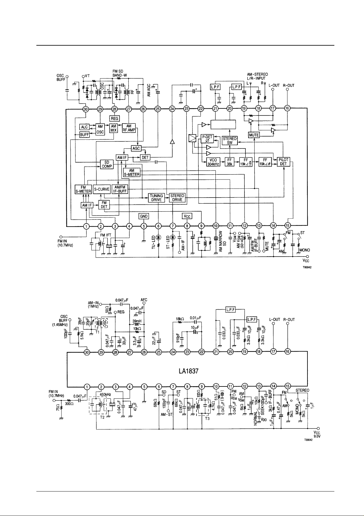
Block Diagram
No. 5688-3/9
LA1837
Test Circuit Diagram
FM SD
ADJ
3 rd 5 th
DECODER
ANTI-BIRDIE
FM
Page 4
Pin No. Pin function Pin voltage (V) Pin description Equivalent circuit
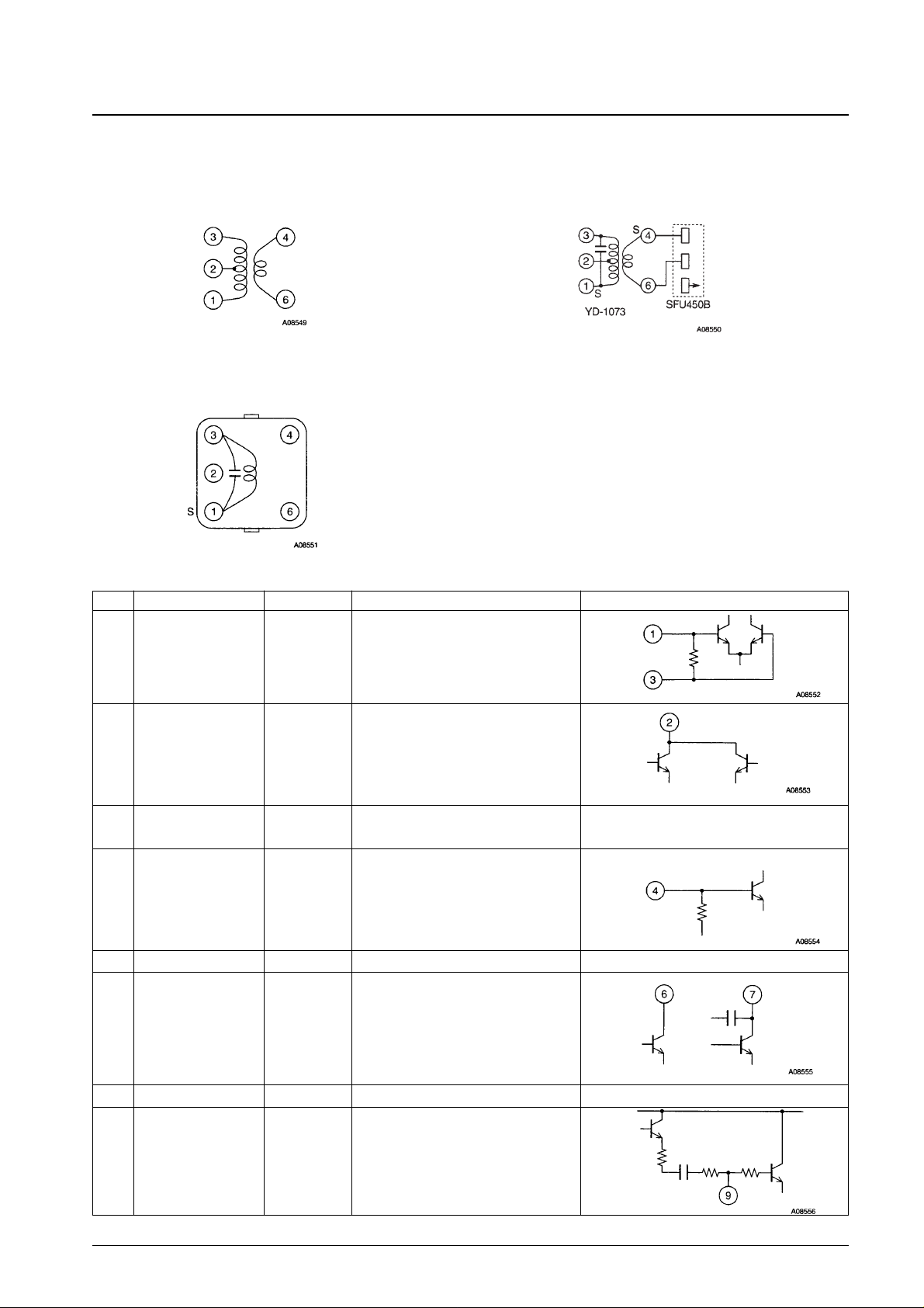
Coil Specifications
No. 5688-4/9
LA1837
· AM oscillator (for the DUT)
HW-50425 (Mitsumi Electric Co., Ltd.)
· IFT
YD-1073-1 (Mitsumi Electric Co., Ltd.)
· FM detector
600BEAS-9715Z (The Toko Electric Corporation)
Pin Functions
1
FM IF input
Vreg
2
AM mixer output
V
CC
Input impedance ri = 330 Ω
Connect the mixer coil between this pin and
V
CC
.
3 FM IF input bypass
Vreg
Also functions as the MPX regulator filter.
4
5
6
7
8
9
AM IF input
GND
TU - LED
ST - LED
AM-IF output
V
CC
FM detector
Vreg
0 V
V
CC
V
CC
V
CC
V
CC
Input impedance ri = 2 kΩ
Active low
Open collector output
AM stereo IF output (pin 7)
The current input must not exceed 150 µA.
Recommended detector coil: 600BEAS9715Z
(The Toko Electric Corporation)
See pin 1.
Continued on next page.
➂ - ➁ 2T
➃ - ➅ 9T
➁ - ➀ 86T
QO ≥ 80
L = 270 µH
➀ - ➁ 58T
➃ - ➅ 7T
➁ - ➂ 94T
fO= 450 kHz
QO= 110
Includes an internal
180-pF capacitor.
SFU450B included.
➂ - ➀ 22T
f = 10.7 MHz
QO = 40
Includes an internal
82-pF capacitor.
Page 5
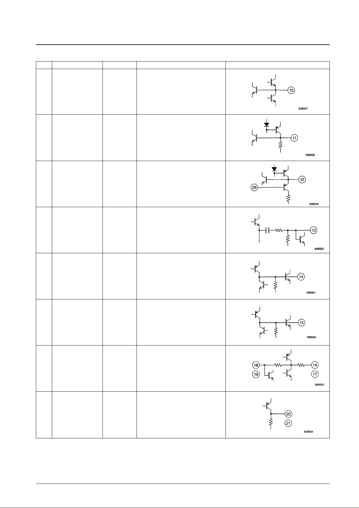
Pin No. Pin Function Pin voltage (V) Pin description Equivalent circuit
No. 5688-5/9
LA1837
AM narrow band CF
connection
1.3 V
Recommended narrow band CF: BFU450
C4N (Murata Mfg. Co., Ltd.)
If the narrow band SD is not used, bypass
this circuit with a 50-Ω resistor and a 0.047µF capacitor connected in series.
10
FM S-meter output 0 V
R
L
= 8 kΩ
11
AM S-meter output
AM SD sensitivity
adjustment
0 V (AM)
The AM SD sensitivity is adjusted with the
value of the external resistor connected
between this pin and ground.
12
AM and FM IF buffer
output, output control
switch (mute switch)
0 V
V13 ≤ 0.5 V: Reception state
1.4 V ≤ V13 ≤ 2.2 V: IF buffer output turned
on
V13 ≥ 3.5 V:
IF buffer output and muting are
turned on
13
Phase comparator
low-pass filter
(FM/AM switching)
V
CC
– 1.4 (FM)
0 V (AM)
Connecting this pin to ground through a
resistor sets the IC to AM mode.
Resistor value limits:
2.7 kΩ (when V
CC
= 7 V)
3.9 kΩ (8 V) 5.1 kΩ(9 V)
6.2 kΩ(10 V) 7.5 kΩ (11 V)
14
Pilot detector low-pass
filter (forced mono)
(VCO stop)
V
CC
– 1.0
If a current of 50 µA or greater flows from
this pin, the system is forced to mono.
Connecting this pin to ground stops the
VCO.
The resistor limit values are the same as for
pin 14.
15
Post amplifier input and
output
Vreg
Vreg
Output impedance r
o
= 200 Ω
Pin 16: right output, pin 17: left output
Inverting inputs
Pin 18: right input, pin 19: left input
R
NF
= 33 kΩ
16
17
18
19
MPX output
3.5 V
3.5 V
Output impedance r
o
= 3.3 kΩ
Pin 20: right de-emphasis
Pin 21: left de-emphasis
20
21
Continued on next page.
Continued from preceding page.
Page 6
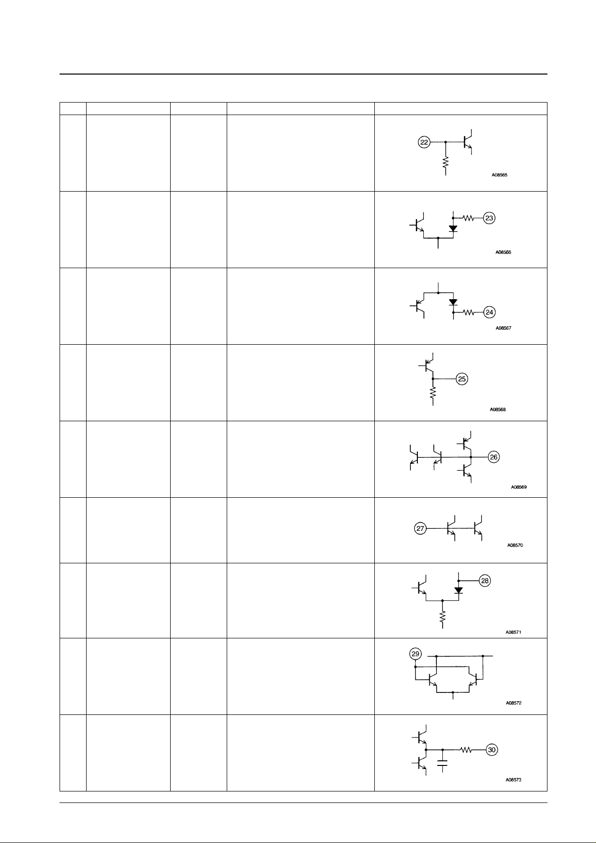
No. 5688-6/9
LA1837
Continued from preceding page.
Pin No. Pin Function Pin voltage (V) Pin description Equivalent circuit
MPX input 2.9 V
Input impedance ri= 20 kΩ
22
FM demodulator output
2.8 V (FM)
2.8 V (AM)
Output impedance r
o
= 3.0 kΩ
The separation can be modified by inserting
a capacitor between this pin and ground.
Set V
O
sub/VOmain to be about 0 dB.
23
AM detector output
0 V (FM)
0.5 V (AM)
Output impedance r
o
= 3.3 kΩ
The AM frequency characteristics can be
modified by adjusting the time constants of
the circuits between this pin and pin 22, and
between this pin and ground.
24
AM AGC
0 V (FM)
0.5 V (AM)
The built-in load resistor R = 11 kΩ.25
AFC Vreg
The FM SD bandwidth can be modified with
the external resistor connected between
this pin and pin 28.
26
AM RF input Vreg Use this pin at the same potential as pin 28.27
REG Vreg Vreg = 3.6 V28
OSC Vreg
Use an oscillator coil between this pin and
pin 28.
29
Oscillator buffer output,
FM SD sensitivity
adjustment
1.6 V (FM)
1.3 V (AM)
The FM SD sensitivity can be modified with
the external resistor connected between
this pin and ground.
Output impedance r
o
= 20 Ω
30
Page 7
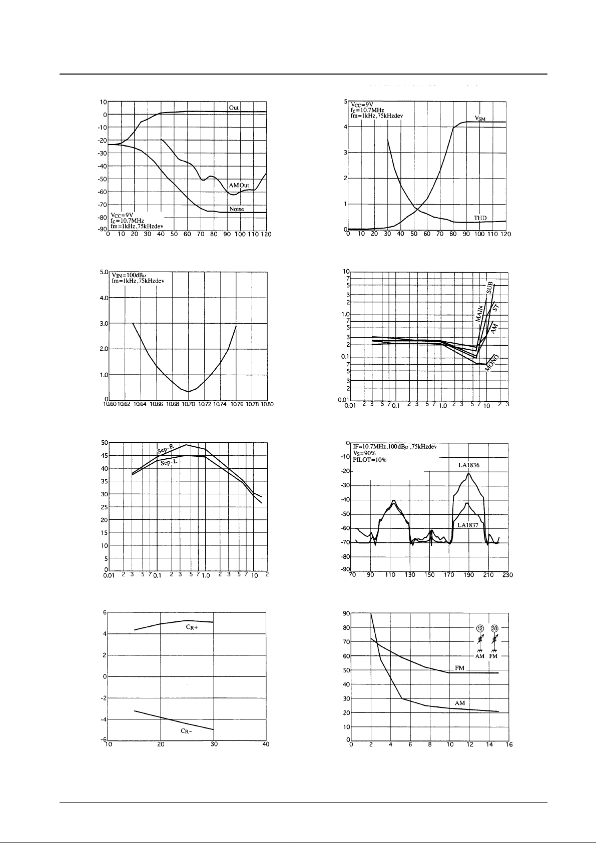
No. 5688-7/9
LA1837
Output – dBm
Input – dBµ
Overall FM Characteristics
Total harmonic distortion, THD – %
S-meter output, V
SM
– V
Iinput – dBµ
FM THD/VSM Characteristics
Total harmonic distortion, THD – %
Frequency, fC– MHz
FM THD Band Characteristics
Total harmonic distortion, THD – %
Frequency, freq – kHz
Distortion vs. Frequency Characteristics
Separation – dB
Frequency, freq – kHz
Separation vs. Frequency Characteristics
Vobat – dB
Frequency, fS– Hz
Adjacent Channel Interference Rejection Ratio
Capture range – %
Pilot – mV
Capture Range Characteristics
SD on – dBµ
Rsdadj – kΩ
SD Sensitivity Adjustment Characteristics
Referenced to the L-R
demodulated output.
FM THD/VSMCharacteristics
Page 8
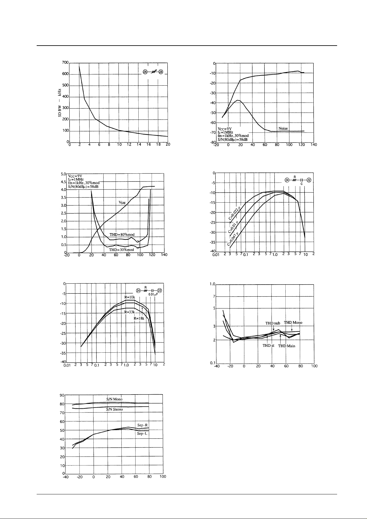
No. 5688-8/9
LA1837
SD BW – kHz
Radj – kΩ
SD Sensitivity Adjustment Characteristics
Total harmonic distortion, THD – %
S-meter output, V
SM
– V
Input – dBµ
AM THD/VSMCharacteristics
Output – dBm
Input – dBµ
Overall AM Characteristics
Output voltage, V
O
–dBV
Frequency, fm – kHz
AM Detector Output Frequency Characteristics (1)
Output voltage, V
O
–dBV
Frequency, fm – kHz
AM Detector Output Frequency Characteristics (2)
Separation, Sep – dB
S/N – dB
Ambient temperature, Ta – °C
Separation vs. Ambient Temperature Characteristics
Total harmonic distortion, THD – %
Ambient temperature, Ta – °C
Distortion vs. Ambient Temperature Characteristics
Output
Page 9

No. 5688-9/9
LA1837
This catalog provides information as of August, 1997. Specifications and information herein are subject to
change without notice.
■ No products described or contained herein are intended for use in surgical implants, life-support systems, aerospace
equipment, nuclear power control systems, vehicles, disaster/crime-prevention equipment and the like, the failure of
which may directly or indirectly cause injury, death or property loss.
■ Anyone purchasing any products described or contained herein for an above-mentioned use shall:
➀ Accept full responsibility and indemnify and defend SANYO ELECTRIC CO., LTD., its affiliates, subsidiaries and
distributors and all their officers and employees, jointly and severally, against any and all claims and litigation and all
damages, cost and expenses associated with such use:
➁ Not impose any responsibility for any fault or negligence which may be cited in any such claim or litigation on
SANYO ELECTRIC CO., LTD., its affiliates, subsidiaries and distributors or any of their officers and employees
jointly or severally.
■ Information (including circuit diagrams and circuit parameters) herein is for example only; it is not guaranteed for
volume production. SANYO believes information herein is accurate and reliable, but no guarantees are made or implied
regarding its use or any infringements of intellectual property rights or other rights of third parties.
 Loading...