

Page 1
Ordering number : ENN6310A
30300RM (OT) No. 6310-1/14
Overview
The LA1650 and LA1650C receive long-wave time
standard broadcasts (JG2AS in Japan and DCF77 in
Germany) and detect and output the time code multiplexed
on the long-wave time standard broadcast signal. Clocks
can automatically correct their time using the time code
information received by the LA1650 and LA1650C.
Features
• Low-voltage operation (VCCop = 1.2 V and higher)
• Low current drain (500 µA for @ 10 dBµ V input)
• Standby mode current: Less than 1 µA
• High sensitivity (Reception is possible at
Vin = 10 dBµ V.)
• Packages: DIP18 (LA1650)
Chip (LA1650C)
Functions
• RF amplifier, rectifier, detector, time code output,
standby circuit
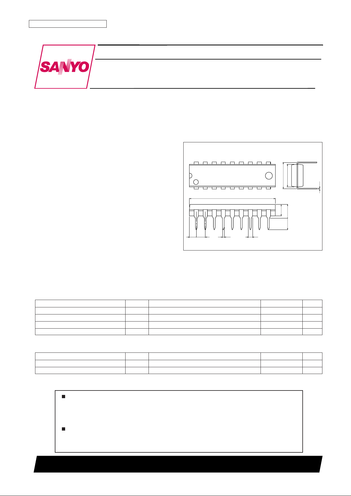
Package Dimensions
unit: mm
3007A-DIP18
1
9
18
10
24.2
1.94 2.54
1.20.5
3.25
3.3
3.85max
0.25
7.62
6.4
SANYO: DIP18
[LA1650]
LA1650, 1650C
SANYO Electric Co.,Ltd. Semiconductor Company
TOKYO OFFICE Tokyo Bldg., 1-10, 1 Chome, Ueno, Taito-ku, TOKYO, 110-8534 JAPAN
Time Code Reception ICs
Monolithic Linear IC
Any and all SANYO products described or contained herein do not have specifications that can handle
applications that require extremely high levels of reliability, such as life-support systems, aircraft’s
control systems, or other applications whose failure can be reasonably expected to result in serious
physical and/or material damage. Consult with your SANYO representative nearest you before using
any SANYO products described or contained herein in such applications.
SANYO assumes no responsibility for equipment failures that result from using products at values that
exceed, even momentarily, rated values (such as maximum ratings, operating condition ranges, or other
parameters) listed in products specifications of any and all SANYO products described or contained
herein.
Parameter Symbol Conditions Ratings Unit
Maximum supply voltage V
CC
max 7.5 V
Allowable power dissipation Pd max Ta ≤ 75°C 100 mW
Operating temperature Topr –20 to +75 °C
Storage temperature Tstg –40 to +125 °C
Specifications
Maximum Ratings at Ta = 25°C
Parameter Symbol Conditions Ratings Unit
Recommended supply voltage V
CC
1.5 V
Operating supply voltage range V
CC
OP 1.2 to 6.5 V
Operating Conditions at Ta = 25°C
Page 2
No. 6310-2/14
LA1650, 1650C
Parameter Symbol Conditions
Ratings
Unit
min typ max
[Overall Characteristics]
Current drain I
CCO
No input 400 540 680 µA
Operating current I
CCfIN
= 40 kHz, VIN= 10 dBµV 370 510 650 µA
Standby current ISTB With the pin 5 (pad 5) voltage at 0 V 0.1 1.0 µA
[Amplifier Input Characteristics]
Input impedance ZI 1pin (PAD1) 450 kΩ
Input frequency range FIN 37.5 80.0 kHz
Minimum input voltage V
IN
min Pin 1 (pad 1) input 1 µVrms
Maximum input voltage V
IN
max Pin 1 (pad 1) input 100 mVrms
[Amplifier Output Characteristics] With pin 1 (pad 1) as the input pin, f
IN
= 40 kHz
Output voltage (1) V
O
1 No input, the pin 11 output 10 20 34 mVrms
Output voltage (2) V
O
2VIN= 10 dBµV, the pin 11 output 15 28 48 mVrms
Output voltage (3) V
O
3VIN= 20 dBµV, the pin 11 output 25 40 62 mVrms
Output voltage (4) V
O
4VIN= 80 dBµV, the pin 11 output 35 48 88 mVrms
[TCO Output Characteristics] With pin 1 (pad 1) as the input pin, f
IN
= 40 kHz
Output voltage (high) V
O
H No input 1.40 1.45 V
Output voltage (low) V
O
LVIN= 10 dBµV 0.05 0.10 V
Output pulse width (500 ms input) T500
V
IN
= 0 to 100 dBµV, AM modulation
480 500 650 ms
(1 Hz square wave, duty = 50%, 100% modulation)
Output pulse width (800 ms input) T800
VIN= 0 to 100 dBµV, AM modulation
750 800 970 ms
(1 Hz square wave, duty = 80%, 100% modulation)
Output pulse width (200 ms input) T200
V
IN
= 0 to 100 dBµV, AM modulation
180 200 400 ms
(1 Hz square wave, duty = 20%, 100% modulation)
Operating Characteristics at Ta = 25°C, VCC= 1.5 V, with the pin 5 used as V
CC,
in the specified test circuit,
unless otherwise specified. Values in parentheses refer to the LA1650C. (Using the Yamaichi Electronics IC37N1803 socket.)
Page 3
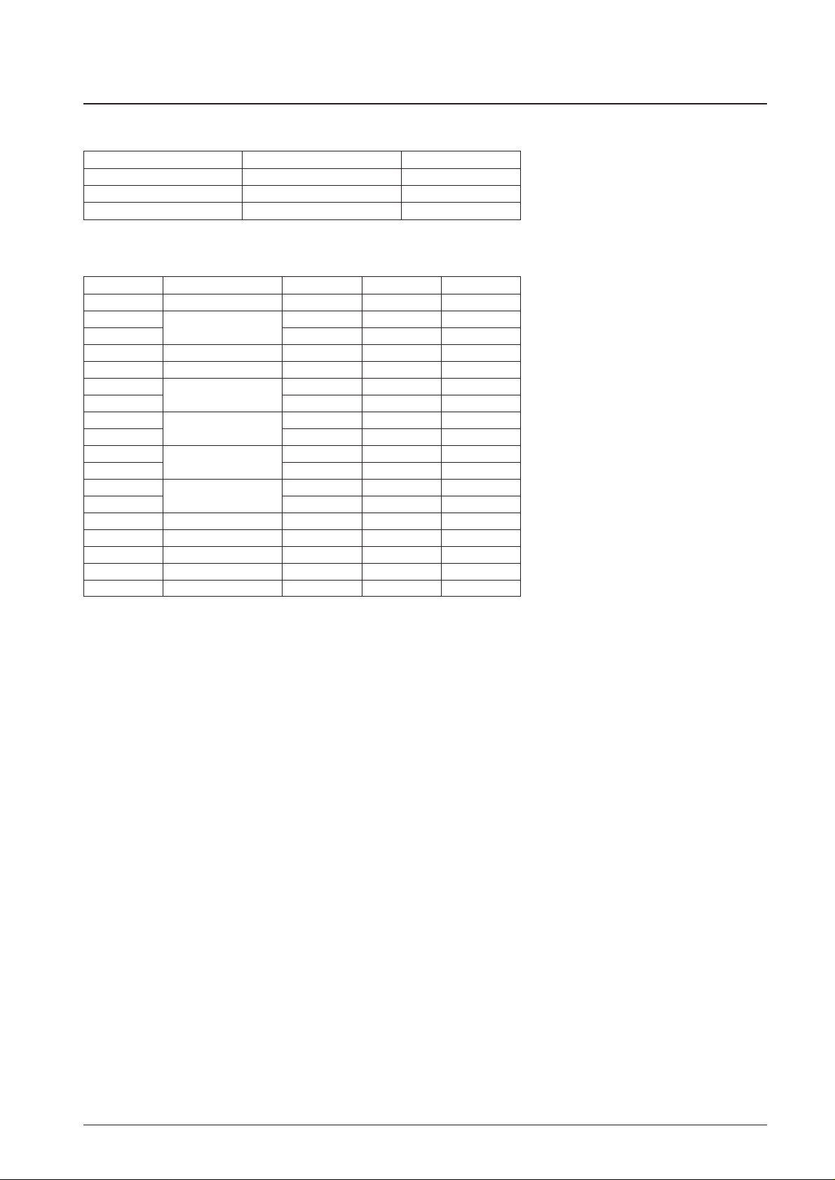
Chip Specifications (LA1650C)
No. 6310-3/14
LA1650, 1650C
Pad Coordinates (LA1650C)
Note: The origin (0, 0) is taken to be the left lower corner in the metal pattern figure on the next page.
The pad coordinates are the values of the coordinates of the center of the pad.
PAD Pad Symbol X-axis Y-axis
P1 Amplifier (1) input INPUT 585 1914
P2
AGC
AGC2 385 1914
P3 AGC1 154 1734
P4 V
CC
V
CC
158 1410
P5 Standby mode PON 154 1221
P6
Amplifier (1) output
AMP1_OUT1 154 711
P7 AMP1_OUT2 164 201
P8
Amplifier (2) input
AMP2_IN1 397 154
P9 AMP2_IN2 597 154
P10
Amplifier (2) output
AMP2_OUT2 864 154
P11 AMP2_OUT1 1086 154
P12
REC input
REC_IN1 1264 361
P13 REC_IN2 1264 531
P14 REC output REC_OUT1 1264 701
P15 DEC input DEC_IN1 1264 1455
P16 DEC output TCO 1264 1625
P17 GND GND 1113 1914
P18 REG REG 849 1914
Chip size 1.41 ×2.06 mm
2
Chip thickness 330 (±20) µm
Pad size 140 × 140 µm
2
Pad opening 115 × 115 µm
2
Page 4
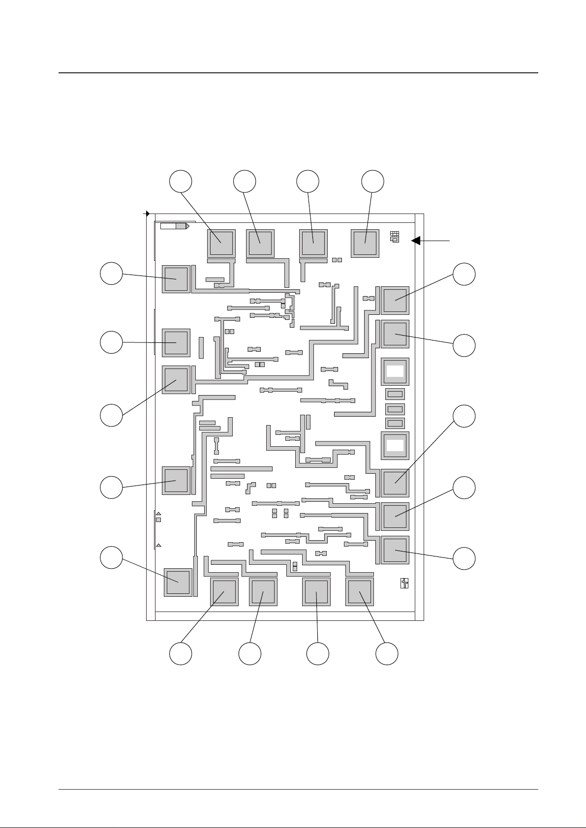
Metal Pattern Figure
No. 6310-4/14
LA1650, 1650C
2 1 18 17
16
1A1650
X : 1.41
Y : 2.06
15
14
13
12
111098
7
6
5
4
3
Pattern
Chip size
1A1650
A12842
NC
NC
Page 5
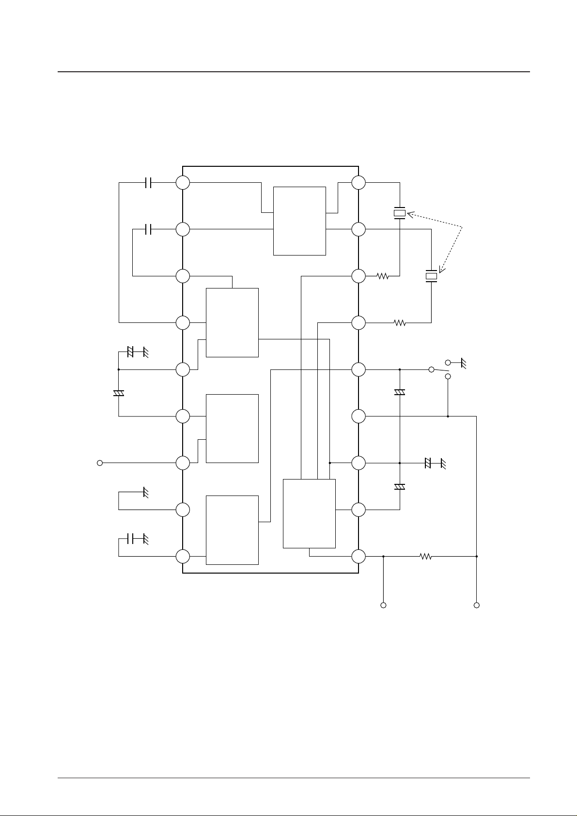
Block Diagram and Test Circuit
No. 6310-5/14
LA1650, 1650C
1
Input
V
CC
2
10µF22µF
10µF
22µF
0.015µF
TCO
1MΩ
1MΩ
1000pF
1000pF
Power ON Standby
40 kHz crystal
100µF
3 4 5 6 7 8 9
18 17 16 15 14 13 12 11 10
AMP(1)
REG DEC
AMP(2)
REC
51Ω
+
+
+
+
+
A12758
Page 6
No. 6310-6/14
LA1650, 1650C
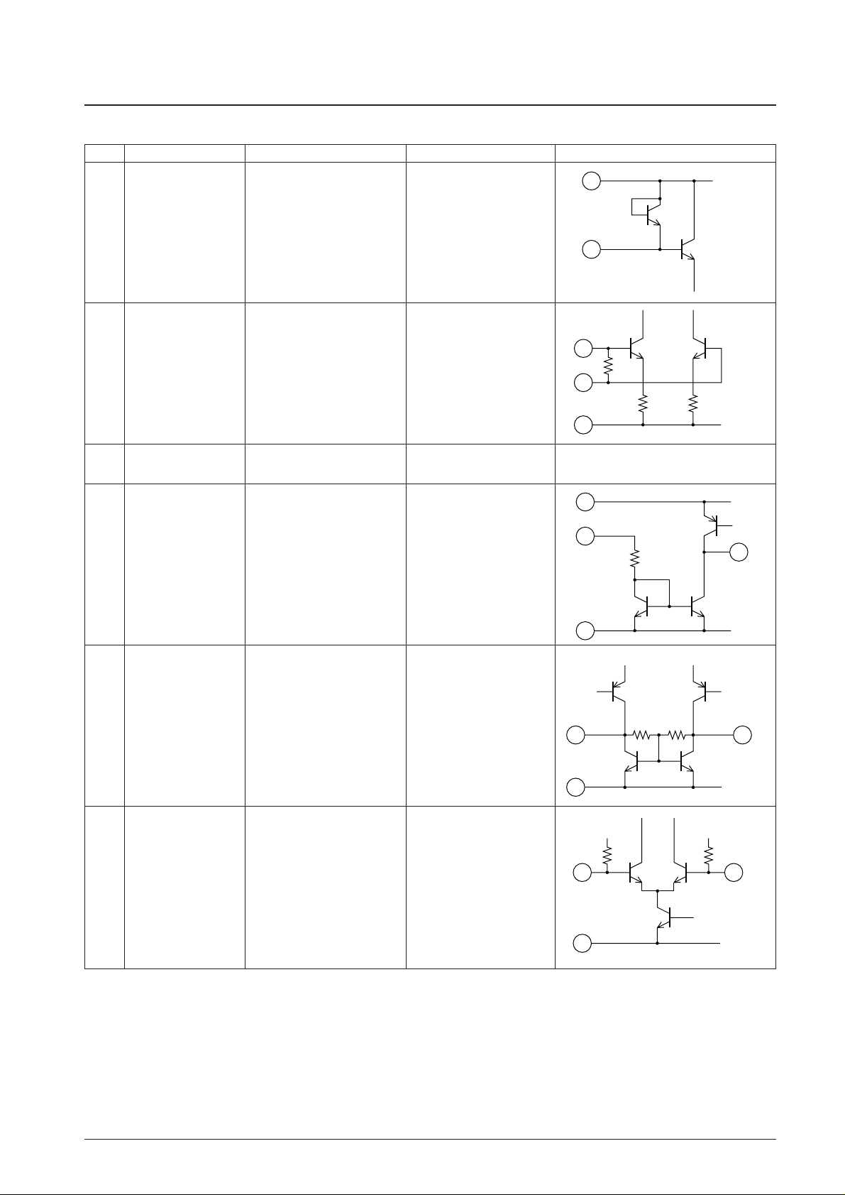
Pin Functions (VCC= 1.5 V)
Pin No. Function No-signal voltage (V) Notes Equivalent circuit
1.5
The input impedance, Zi, is
450 kΩ.
Connect the antenna coil
between pins 1 and 4.
Recommended coil: ACL-80
(Sumida Electronics)
1 Amplifier (1) input
4
1
A12759
0.6
0.6
The AGC operating speed is
determined by the capacitor
connected between pin 3 and
ground.
2
3
AGC (1) input
AGC (2) input
3
2
17
A12760
1.54
V
CC
1.5
This LA1650 operates normally
with pin 5 at V
CC
. The device
goes to standby mode (I
CC
≤ 1
µA) when this pin is pulled to
ground.
5 PON
4
5
18
17
A12761
0.7
Connect the crystal oscillator
elements between pins 6 and 8,
and pins 7 and 9.
Recommended element: VTC200 (Seiko Instruments)
40 kHz, 12.5 pF
6
7
Amplifier (1) output
6 7
17
A12762
0.8
RIN= 20 kΩ
8
9
Amplifier (2) input
8
R
IN
R
IN
17
9
A12763
Continued on next page.
Page 7
No. 6310-7/14
LA1650, 1650C
Continued from preceding page.
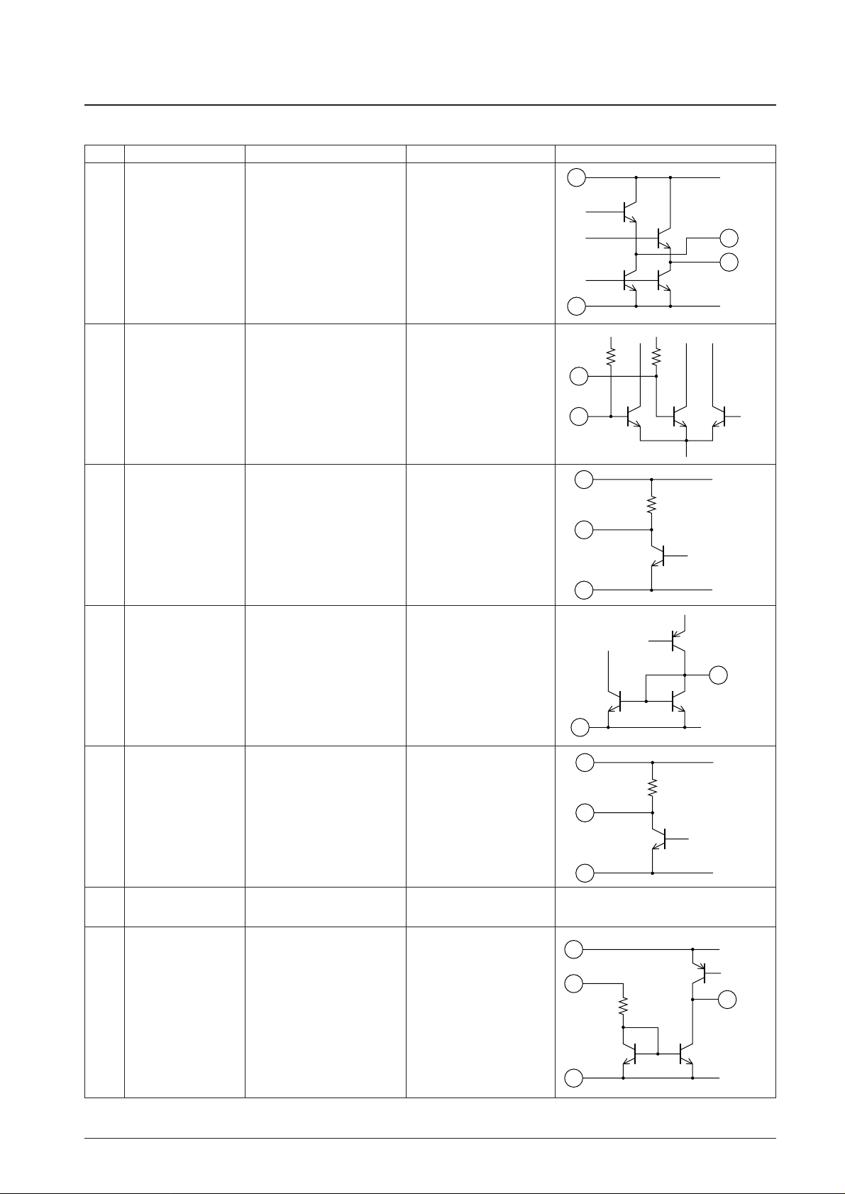
Pin No. Function No-signal voltage (V) Notes Equivalent circuit
0.7 Emitter-follower output
10
11
Amplifier (2) output
10
11
4
17
A12764
0.8
Full-wave rectifier circuit input
R
IN
= 20 kΩ
12
13
REC input
13
12
R
IN
R
IN
A12765
0.8
Full-wave rectifier circuit output
R
OUT
= 75 kΩ
High-frequency components
are smoothed by the capacitor
connected between pin 14 and
ground.
14 REC output
4
R
OUT
14
17
A12766
0.7 Wave shaping circuit input15 DEC input
17
15
A12767
—
Wave shaping circuit output
R
OUT
= 100 kΩ
This pin outputs the time code.
(Inverted output)
16 DEC output
4
R
OUT
16
17
A12768
017 GND
0.8
Vreg = VCC– 0.7 V
18 REG
4
5
18
17
A12769
Page 8
Block Functional Descriptions
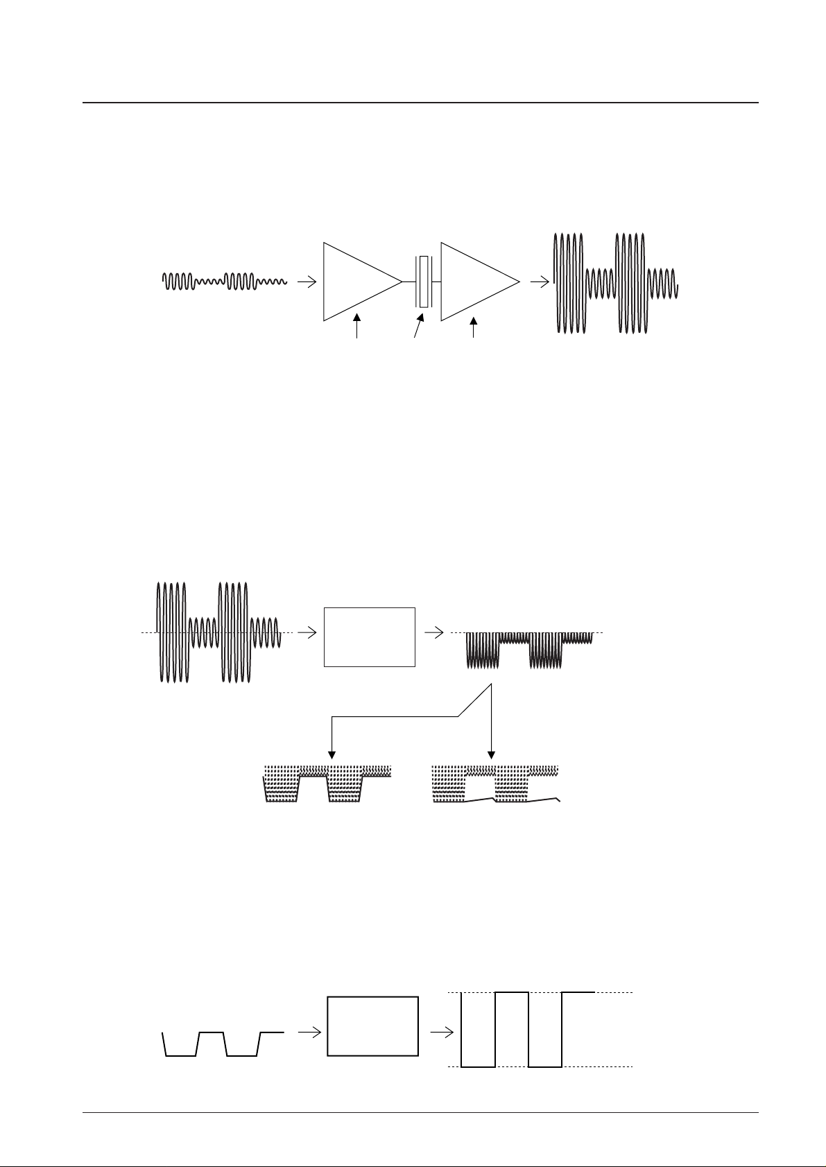
Amplifier Block
The radio signal picked up by the bar antenna (resonant frequency: 40 kHz for Japan) is amplified by amplifier 1 which
includes an AGC function, and is passed through a 40 kHz crystal element used as a bandpass filter. This signal is then
amplified further by amplifier 2. The total gain from the amplifier 1 input to the amplifier 2 output is 90 dB when the
AGC is disabled.
The AGC voltage is set up to be about 0.6 V when there is no input present. However, since charging is performed by a
small current of only a few µA, we recommend precharging if the LA1650 is used for reception immediately after power
is applied. (Charge to about 1.0 V for about 100 ms.)
DEC Block
The time code signal (1 Hz) from which the 40 kHz carrier has been removed is input to the DEC block, and wave
shaping is applied to create a serial output signal in which 1 and 0 have the levels VCCand ground, respectively.
No. 6310-8/14
LA1650, 1650C
AMP(1) witn AGC AMP(2)Crystal
A12770
Since amplifier 1 has frequency characteristics of –3 dB at fc = 80 kHz from the output level at fc = 40 kHz, and
amplifier 2 has frequency characteristics that are flat up to 100 kHz, this IC can support the standard radio frequencies
used in any country simply by changing bar antenna and the resonant frequency of the crystal used.
REC Block
The 40 kHz carrier signal output from amplifier 2 is input to the REC block through a 1000 pF capacitor. The REC block
input impedance is 20 kΩ, which, in conjunction with the 1000 pF capacitor, forms a high-pass filter with a cutoff
frequency of about 8 kHz. The carrier is full-wave rectified within the REC block, split into two signal systems, and
output. One signal system passes through a low-pass filter with a time constant of about 1 s and is then input to the DEC
block. The other passes through a low-pass filter with an even larger time constant and is fed back to amplifier 1 as the
AGC control voltage (pin 3: a DC voltage).
Rectifier
Low-pass filter
(time constant: 1 s)
Low-pass filter
(time constant: several seconds or longer)
To the DEC block AGC voltage (to amplifier 1)
A12771
Decoder
V
CC
GND
A12772
Page 9
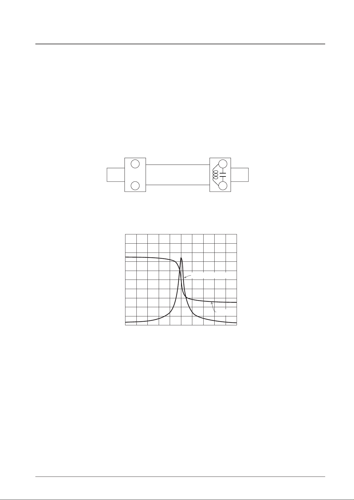
Antenna (prototype) Specifications
Model number: ACL-80 (Sumida Electronics)
Prototype number: 74M-656
Inductance: 588 µH (reference value at 10 kHz)
Tuning frequency: 40 kHz
Mounting capacitance: 27000 pF
Winding: UEW 0.35
Number of windings: 94 turns (4-3)
* Consult with your Sanyo representative before starting mass production.
Pin Connections (back surface)
No. 6310-9/14
LA1650, 1650C
1
2
3
4
S
A12773
0
180
35
–180
10
20
0
40 45
Phase,θ — deg.
Impedance, Z — kΩ
Impedance, Z
Phase, θ
Frequency, f — kHz
θ, Z — f
Page 10
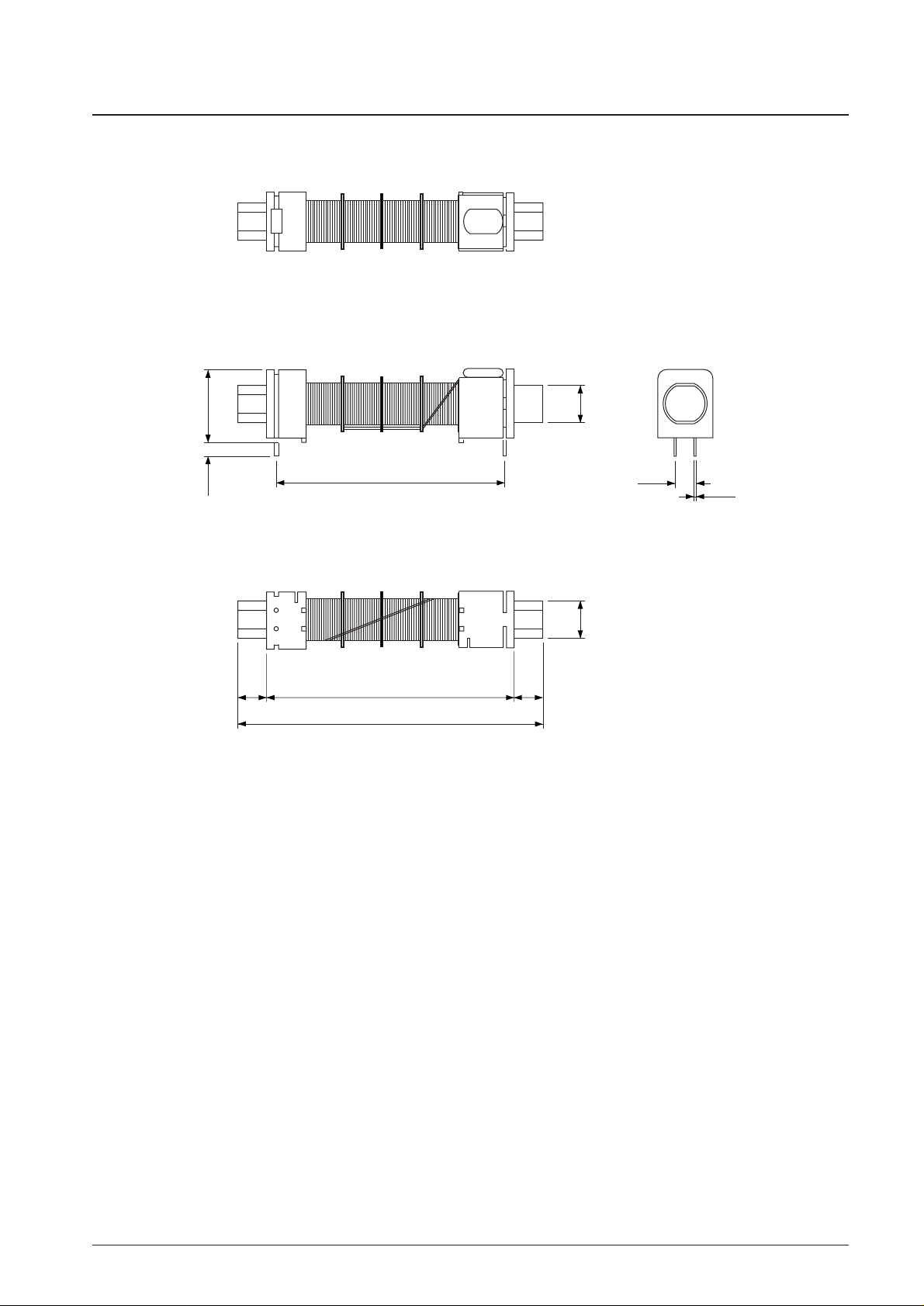
Antenna Dimensions (trigonometric)
No. 6310-10/14
LA1650, 1650C
18.03.5
60.0
5.0
0.7
9.0
ø10.0
7.5 7.5
65.0
80.0
A12843
Page 11
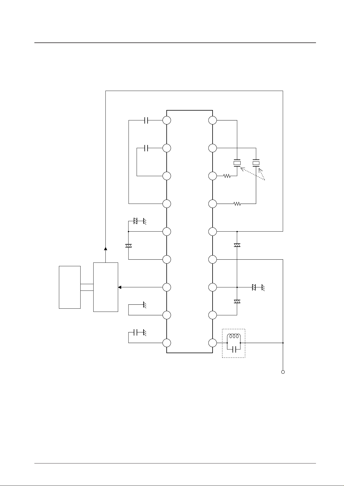
Sample Application Circuit
No. 6310-11/14
LA1650, 1650C
1
V
CC
Bar ANT
2
10µF22µF
10µF
22µF
0.015µF
TCO
PON
1MΩ
1MΩ
1000pF
1000pF
40 kHz crystal
100µF
3 4 5 6 7 8 9
18 17 16 15 14 13 12 11 10
+
+
+
+
+
A12774
Microcontroller
Display
LA1650
Page 12
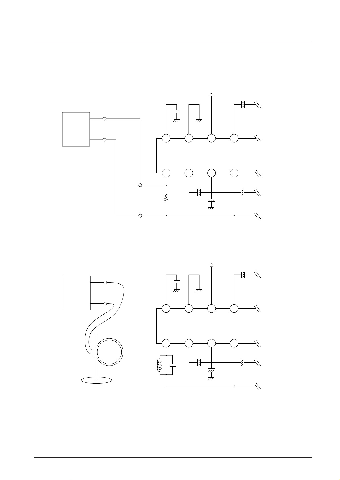
LA1650 Evaluation Procedure
Two relatively simple techniques for measuring the sensitivity index are (1) to input the signal generator output directly
to the IC (see figure 1), and (2) to use an antenna as shown in figure 2.
No. 6310-12/14
LA1650, 1650C
1 2
TCO
3 4
18 17 16 15
+
+
+
+
LA1650
A12776
Bar antenna
Loop antenna
1 2
TCO
51 Ω
SG
3 4
18 17 16 15
+
+
+
+
LA1650
A12775
50 Ω output
SG
Figure 1 Direct Signal Generator Input to the IC
Figure 2 Antenna to Antenna Signal Input
Page 13
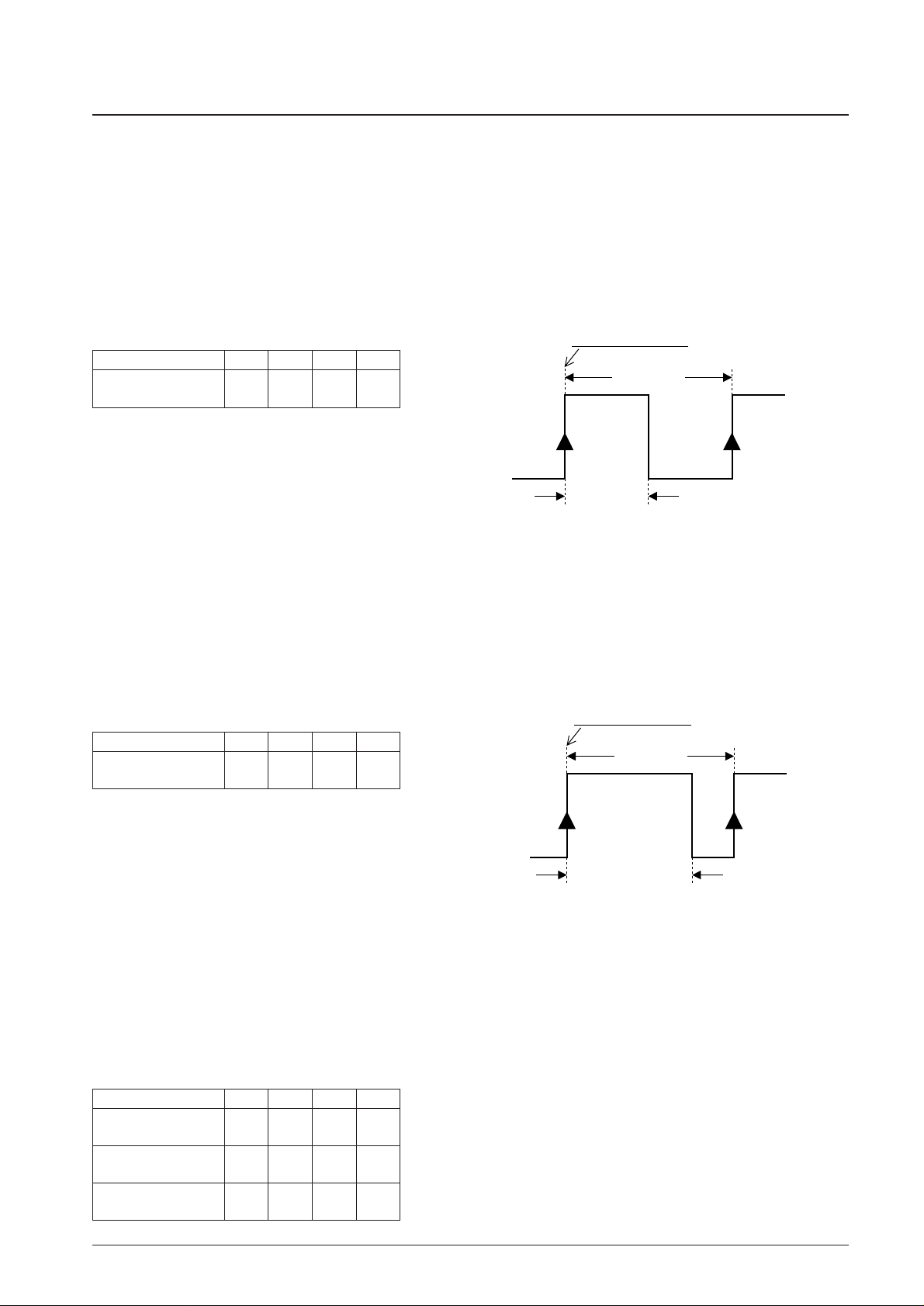
The following three techniques are practical test procedures. Note that since the output from the LA1650 pin 16 is
inverted from the value of the time code, an inverter must be inserted between the output and the microcontroller.
• Continuously output a signal with the value 1 (fc = 40 kHz, AM modulation (90%), fm = 1 Hz (square wave, duty =
50%)) and read out the value 1 from the LA1650. Then, lower the signal generator level until the LA1650 can no
longer correctly output the 1 level. The minimum signal generator level at which correct reception occurs is the
sensitivity.
When monitoring the LA1650 output signal with a microcontroller, monitor the output pulse width for the range listed
in table 1. The output signal should be observed to be a 1 Hz signal, with a period of 1000 ±25 ms. (See figure 3.)
• Continuously output a signal with the value 0 (fc = 40 kHz, AM modulation (90%), fm = 1 Hz (square wave, duty =
80%)) and read out the value 0 from the LA1650. Then, lower the signal generator level until the LA1650 can no
longer correctly output the 0 level. The minimum signal generator level at which correct reception occurs is the
sensitivity.
When monitoring the LA1650 output signal with a microcontroller, monitor the output pulse width for the range listed
in table 2. The output signal should be observed to be a 1 Hz signal, with a period of 1000 ±25 ms. (See figure 4.)
• Create a simulated time standard radio signal (fc = 40 kHz, AM modulation (90%), fm = 1 Hz time code (this signal
you will have to create yourself)) and verify that the time is modified correctly. The sensitivity is then the minimum
level for which the time is modified correctly.
When monitoring the LA1650 output signal with a microcontroller, monitor the output pulse width for the ranges listed
in table 3. The output signal should be observed to be a 1 Hz signal, with a period of 1000 ±25 ms. (See figure 4.)
No. 6310-13/14
LA1650, 1650C
1000 ±25 ms
480 to 650 ms
TCO rise (reference)
A12777
Table 1 Signal Value 1 Range
Item min typ max unit
Output pulse width
480 500 650 ms
(500 ms input)
Table 2 Signal Value 0 Range
Item min typ max unit
Output pulse width
750 800 970 ms
(800 ms input)
Table 3 Time Code Signal Output Ranges
Item min typ max unit
Output pulse width
480 500 650 ms
(500 ms input)
Output pulse width
750 800 970 ms
(800 ms input)
Output pulse width
180 200 400 ms
(200 ms input)
Figure 3 Time Code Value 1 Signal Output
Figure 4 Time Code Value 0 Signal Output
TCO rise (reference)
1000 ±25 ms
750 to 970 ms
A12778
Page 14
PS No. 6310-14/14
LA1650, 1650C
This catalog provides information as of March, 2000. Specifications and information herein are subject to
change without notice.
Specifications of any and all SANYO products described or contained herein stipulate the performance,
characteristics, and functions of the described products in the independent state, and are not guarantees
of the performance, characteristics, and functions of the described products as mounted in the customer’s
products or equipment. To verify symptoms and states that cannot be evaluated in an independent device,
the customer should always evaluate and test devices mounted in the customer’s products or equipment.
SANYO Electric Co., Ltd. strives to supply high-quality high-reliability products. However, any and all
semiconductor products fail with some probability. It is possible that these probabilistic failures could
give rise to accidents or events that could endanger human lives, that could give rise to smoke or fire,
or that could cause damage to other property. When designing equipment, adopt safety measures so
that these kinds of accidents or events cannot occur. Such measures include but are not limited to protective
circuits and error prevention circuits for safe design, redundant design, and structural design.
In the event that any or all SANYO products (including technical data, services) described or contained
herein are controlled under any of applicable local export control laws and regulations, such products must
not be exported without obtaining the export license from the authorities concerned in accordance with the
above law.
No part of this publication may be reproduced or transmitted in any form or by any means, electronic or
mechanical, including photocopying and recording, or any information storage or retrieval system,
or otherwise, without the prior written permission of SANYO Electric Co., Ltd.
Any and all information described or contained herein are subject to change without notice due to
product/technology improvement, etc. When designing equipment, refer to the “Delivery Specification”
for the SANYO product that you intend to use.
Information (including circuit diagrams and circuit parameters) herein is for example only; it is not
guaranteed for volume production. SANYO believes information herein is accurate and reliable, but
no guarantees are made or implied regarding its use or any infringements of intellectual property rights
or other rights of third parties.
 Loading...