

Page 1

LA1600
Ordering number : EN2056B
1-Band AM Radio
Monolithic Linear IC
SANYO Electric Co.,Ltd. Semiconductor Bussiness Headquarters
TOKYO OFFICE Tokyo Bldg., 1-10, 1 Chome, Ueno, Taito-ku, TOKYO, 110 JAPAN
D2797HA (KT)/41594HK/O077KI/4236KI, TS No.2056-1/7
Overview
The LA1600, being an AM tuner IC placed in a 9-pin SIP,
provides the functions of an AM tuner. It is usable in the
band range up to SW band and is especially suited for use
in low-cost AM radios and radio-controlled receivers.
Functions
• AM : RF amp, MIX, OSC, IF amp, detector, AGC.
Features
• Minimum number of external parts required.
• Low current drain (3.7mA).
• Low supply voltage (1.8V min).
• Adoption of double-balanced mixer.
• Usable in the band range up to SW band.
Specifications
Maximum Ratings
at Ta=25°C, See specified Test Circuit.
Parameter Symbol Conditions Ratings Unit
Maximum supply voltage VCCmax Pin 3 9 V
Pin 4 9 V
Pin 8 7 V
Allowable power dissipation Pd max Ta≤70°C 100 mW
Operating temperature Topr –20 to +70 °C
Storage temperature Tstg –40 to +125 °C
Operating Conditions at Ta=25°C
Parameter Symbol Conditions Ratings Unit
Recommended operating voltage V
CC
3V
Operating voltage range V
CC
op 1.8 to 6.0 V
Operating Characteristics at Ta=25°C, V
CC
=3V, See specified Test Circuit.
Parameter Symbol Conditions
Ratings
min typ max
Unit
[AM Characteristics/f=1MHz]
Quiescent current Icco VIN=No input 3.7 4.6 mA
Detection output VO1V
IN
=23dBµ, 1kHz-30% mod –30 –25 –20 dBm
24 43 78 mV
VO2V
IN
=80dBµ, 1kHz-30% mod –18 –14 –10 dBm
97 155 250 mV
S/N S/N1 VIN=23dBµ 18 21.5 dB
S/N2 VIN=80dBµ 48 53 dB
Total harmonic distortion THD1 VIN=80dBµ, 1kHz-30% mod 0.3 1.2 %
THD2 V
IN
=100dBµ, 1kHz-30% mod 0.4 1.5 %
Package Dimensions
unit : mm
3017B-SIP9
[LA1600]
SANYO : SIP9
0.99
0.25
1.35
3.0
22.3
0.51min
5.7max
3.2
1.5
4.8
1.0
2.54
1.3
0.5
1
9
Page 2

LA1600
No.2056-2/7
Equivalent Circuit Block Diagram
IFT (Intermediate Frequency Transformer)
Specified Test Circuit Diagram
Test Circuit 1 :AM-MW
Unit (resistance : Ω, capacitance : F)
Unit (resistance : Ω, capacitance : F)
Unit (resistance : Ω, capacitance : F)
1. Using double tuning coil 2. Using ceramic filter
(Sumida)
(Mitsumi)
(Mitsumi)
(Mitsumi)
(Sumida)
(for PVC22KTL)
Page 3

LA1600
No.2056-3/7
MW Input/Output Characteristics 1
Antenna input voltage – dB/m
Antenna input voltage – dB/m
Antenna input voltage – dB/m
Noise voltage, Detection output – dBm
Total harmonic distortion, THD – %
Current drain, I
CC
– mA
Total harmonic distortion, THD – %
Detection output, Whistle output – dBm
Receiving frequency, fr– kHz
Sensitivity – dB/m Interference – dB
Current Drain, Pin 6 Voltage Characteristics
Whistle Characteristics
Selectivity Characteristic
Spurious Response
Pin 6 voltage – V
MW Reception Characteristics
Attenuation – dB
MW Fidelity Characteristics
Modulation frequency – Hz
Frequency, ∆f – kHz
Attenuation – dB
Noise voltage 1kHz-30% mod
fIN=1MHz
Input=100dB/m
Attenuation
Current drain
Detection output (1kHz-30%)
Frequency, f – Hz
Response – dB
VCCCharacteristics
Supply voltage, VCC– V
Pin 6 voltage – V
Detection output – dBm
Current drain, I
CC
– mA
1MHz reception
ICCno input
Detection output
Distortion
Output=20mV
const.
Pin 6 voltage
Whistle max.
Tracking adjust at each frequency.
IF interference
Image frequency interference
Usable
sensitivity
(1kHz-30% mod, S/N=20dB)
Max. sensitivity
(1kHz-30% mod, detection output 20mV)
Sensitivity – dB/m
Detection output (1kHz-30% mod, 100dB/m)
Sensitivity (1kHz-30% mod, output 20mV)
quiescent
1MHz reception
Page 4
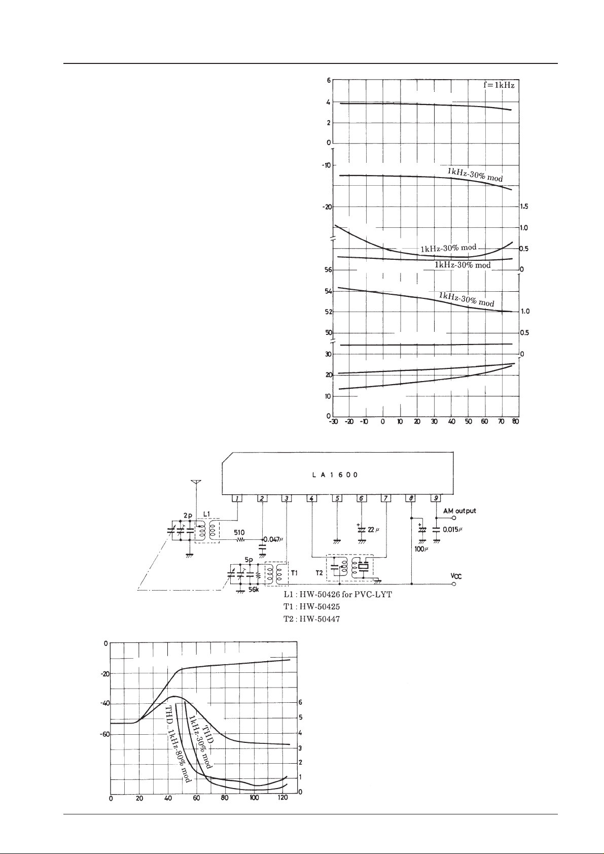
LA1600
No.2056-4/7
Pin 6 voltage – V Distortion – %
Temperature Characteristics
Ambient temperature, Ta – °C
Sensitivity – dBµ
S/N – dB
Current drain, I
CC
– mA
Detection output – dBm
I
CC
quiescent
Detection output input 80dBµ
THD input 100dBµ
THD input 80dBµ
S/N input 80dBµ
V6 quiescent
S/N=20dB sensitivity 1kHz-30% mod
Output 20mV
sensitivity
Test Circuit 2 :AM-MW
(Mitsumi)
(Mitsumi)
(Mitsumi)
Unit (resistance : Ω, capacitance : F)
MW Input/Output Characteristics 2
Antenna input voltage – dB/m
Noise voltage, Detection output – dBm
Total harmonic distortion, THD – %
Noise voltage
Detection output 1kHz-30% mod
1MHz reception
1kHz-30% mod
Page 5
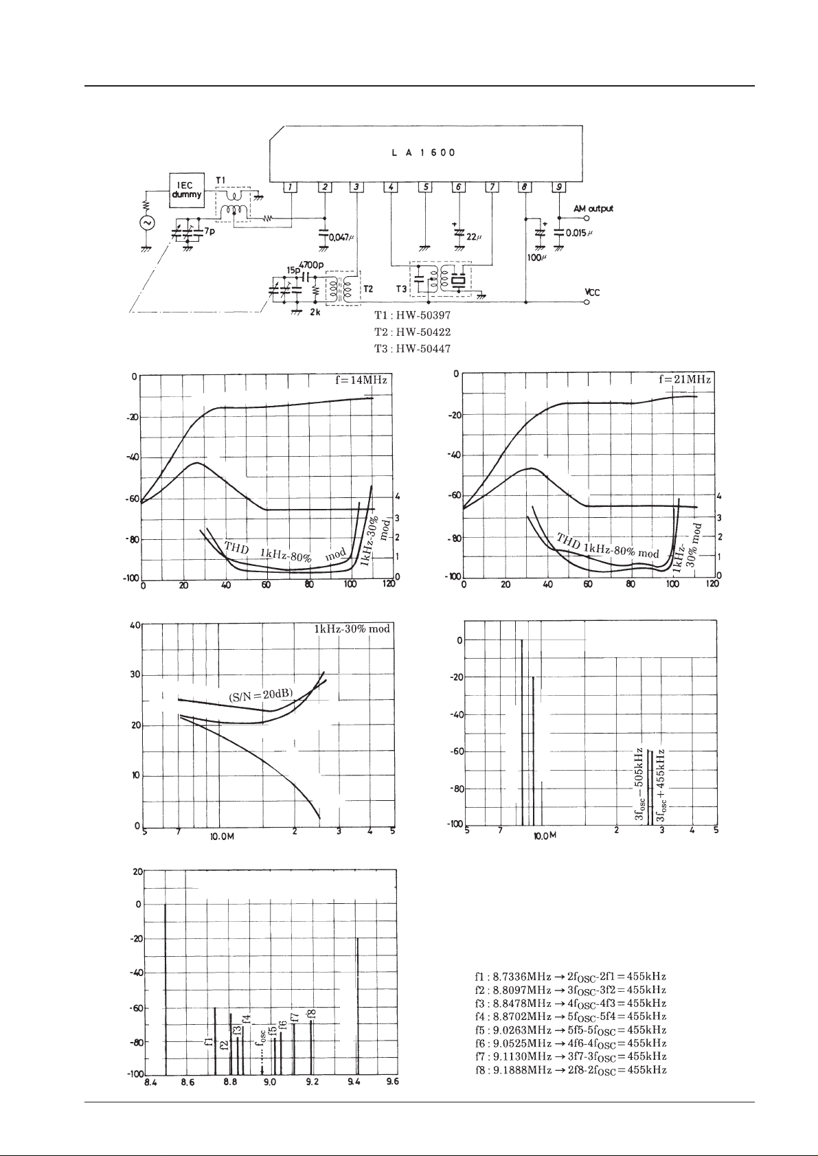
LA1600
No.2056-5/7
Unit (resistance : Ω, capacitance : F)
Test Circuit 3 :SW2 (7.2 to 24.0MHz)
(Mitsumi)
(Mitsumi)
(Mitsumi)
SW2 Input/Output Characteristics
IEC input voltage – dBµ
Noise voltage, Detection output – dBm
Sensitivity – dBµ
Total harmonic distortion, THD – %
Noise voltage
Detection output 1kHz-30% mod
SW2 Reception Characteristics
Receiving frequency, fr– Hz
Image frequency
interference – dB
Max. sensitivity
(Input at
Usable sensitivity
SW2 Input/Output Characteristics
IEC input voltage – dBµ
Noise voltage, Detection output – dBm
Total harmonic distortion, THD – %
Noise voltage
Detection output 1kHz-30% mod
detection output
–30dBm)
Image frequency
interference
Spurious – dB
8.5MHz Spurious Response
Frequency, f – MHz
Receiving frequency
Output –30dBm
(Referenced to ANT input
21dBµ-8.5MHz)
Image frequency
Spurious – dB
8.5 to 9.4MHz Spurious – dB
Receiving frequency, fr– MHz
Receiving frequency
Output –30dBm
(Referenced to ANT input 21dBµ-8.5MHz)
Image frequency
Page 6
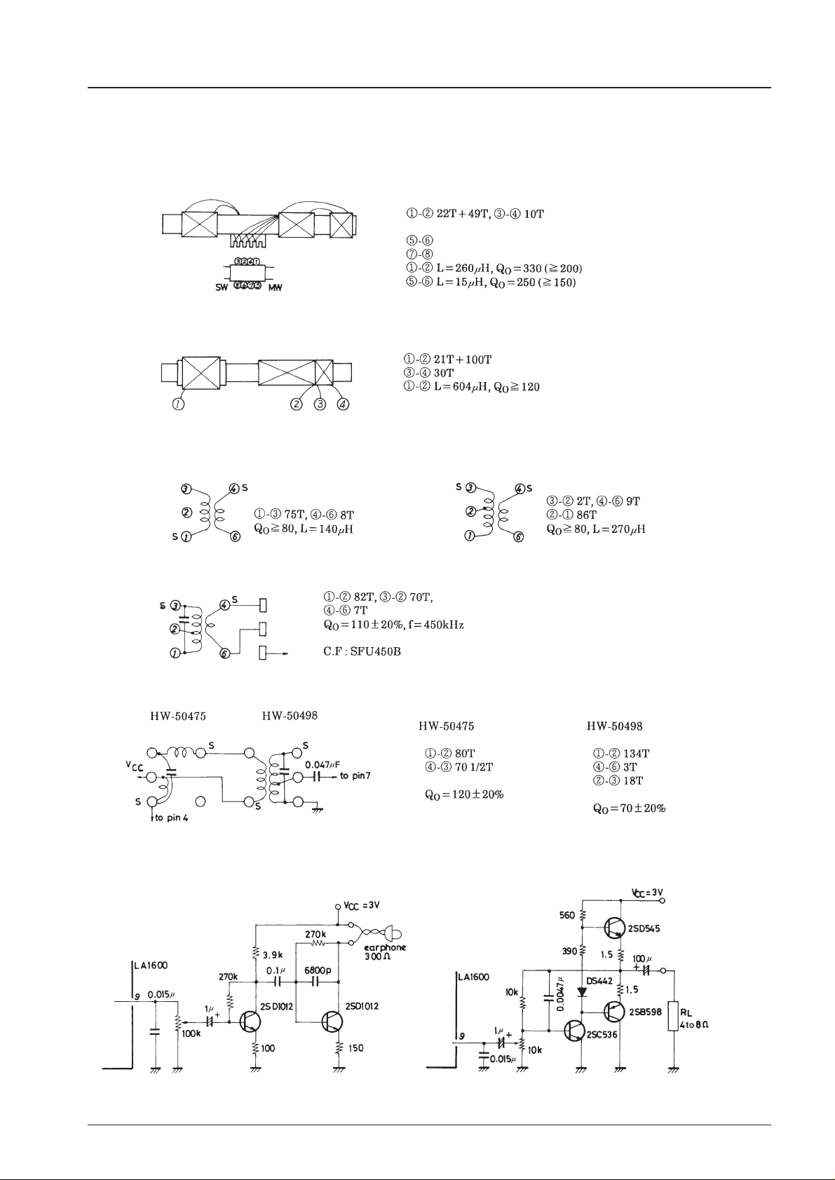
LA1600
No.2056-6/7
Coil Specifications
MW antenna
Bar antenna (for PVC22KTL)
• TN-10896 (Mitsumi)
Tight solenoid direct winding
17T 0.5φ space winding
4T tight solenoid winding
Bar antenna (for PVC-LYT)
• HW-50426 (Mitsumi)
MW OSC
• S-190-036 (Sumida)
For PVC22KTL
• HW-50426 (Mitsumi)
For PVC-LYT
(Mitsumi)
Internal 180pF
AM-IFT
• HW-50447 (Mitsumi)
AM-IFT
Application where a double tuning coil is used
Internal 180pF
(Mitsumi)
Internal 180pF
Sample Application Circuit 1
Earphone
Transistor rank=G280 to 560
Sample Application Circuit 2
Power amp using 3 discrete devices
Transistor rank=E100 to 200
Unit (resistance : Ω, capacitance : F)
Page 7
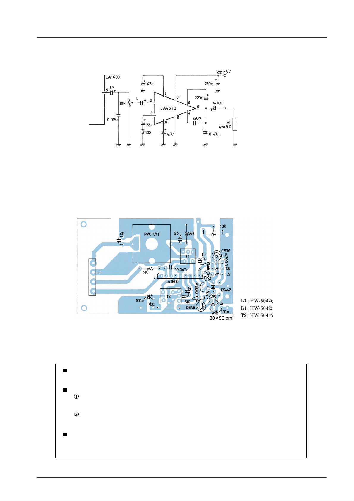
LA1600
No.2056-7/7
Sample Application Circuit 3
Using the LA4510
Sample Printed Circuit Pattern : LA1600 + Power amp using 3 discrete devices
(For the circuit diagram, refer to Test Circuit 2 and Sample Application
Circuit 2.)
Unit (resistance : Ω, capacitance : F)
(Mitsumi)
(Mitsumi)
(Mitsumi)
No products described or contained herein are intended for use in surgical implants, life-support systems,
aerospace equipment, nuclear power control systems, vehicles, disaster/crime-prevention equipment and
the like, the failure of which may directly or indirectly cause injury, death or property loss.
Anyone purchasing any products described or contained herein for an above-mentioned use shall:
Accept full responsibility and indemnify and defend SANYO ELECTRIC CO., LTD., its affiliates,
subsidiaries and distributors and all their officers and employees, jointly and severally, against any
and all claims and litigation and all damages, cost and expenses associated with such use:
Not impose any responsibilty for any fault or negligence which may be cited in any such claim or
litigation on SANYO ELECTRIC CO., LTD., its affiliates, subsidiaries and distributors or any of
their officers and employees jointly or severally.
Information (including circuit diagrams and circuit parameters) herein is for example only; it is not guaranteed for volume production. SANYO believes information herein is accurate and reliable, but no guarantees
are made or implied regarding its use or any infringements of intellectual property rights or other rights of
third parties.
This catalog provides information as of December, 1997. Specifications and information herein are subject
to change without notice.
 Loading...