

Page 1
Ordering number: EN 2725A
Monolithic Linear IC
LA1145, 1145M
FM IF System (Quadrature Detector) for Car Radio
Features
1. On-chip IF count buffer circuit and microprocessorcontrolled switch circuit for ETR.
2. Compared to the LA1140, the LA1145, 1145M offer:
1 Improved signal meter output linearity;
2 Improved band mute temperature stability;
3 Improved S/N ratio;
4 Improved sound quality at weak signal input when
noise is present, and;
5 Improved AMR characteristics during weak signal
input.
3. Reduced parts’ count simplifies design:
1 On-chip IF count buffer circuit;
2 On-chip SD circuit — sensitivity can be set
independently of soft mute characteristics, and;
3 Variable S-meter gradient — three pin S-meter output
(pins 5, 16 and 17) facilitates independent control of
SNC and HCC.
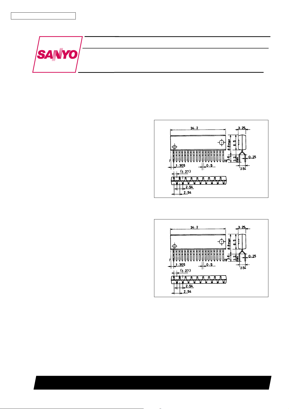
Package Dimensions
unit : mm
3115-SIP18Z
[LA1145]
SANYO : SIP18Z
unit : mm
3036B-MFP20
[LA1145M]
SANYO: MFP20
SANYO Electric Co.,Ltd. Semiconductor Bussiness Headquarters
TOKYO OFFICE Tokyo Bldg., 1-10, 1 Chome, Ueno, Taito-ku, TOKYO, 110 JAPAN
93097HS(II)/3132TS/2118TA No.2725-1/17
Page 2
LA1145, 1145M
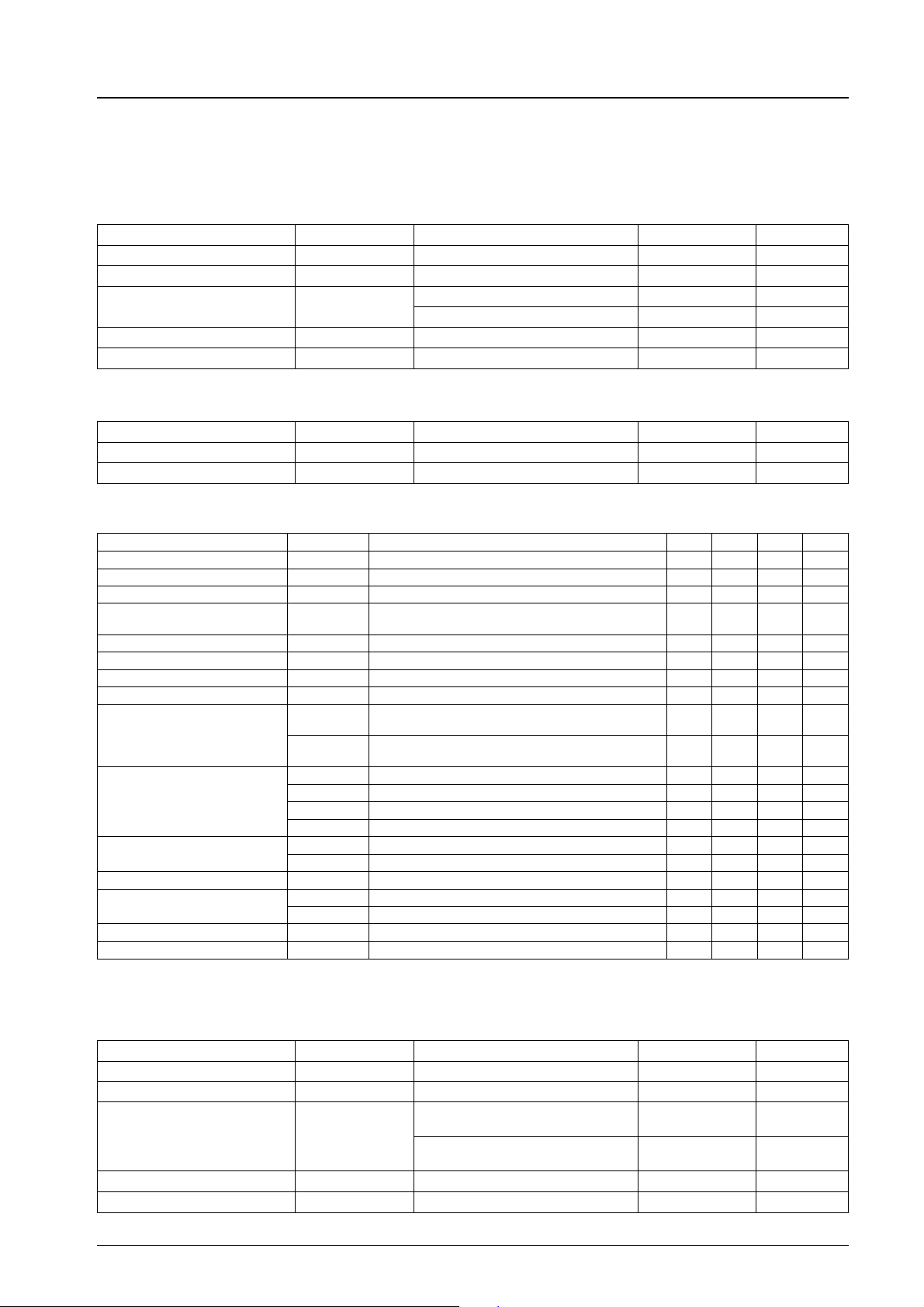
Specifications
[LA1145]
Maximum Ratings atTa=25°C
Parameter Symbol Conditions Ratings Unit
Maximum supply voltage V
Maximum supply current I
Allowable power dissipation Pd max Ta = 65 °C 630 mW
Operating temperature Topr –20 to +70 °C
Storage temperature Tstg –40 to +150 °C
Operating Conditions atTa=25°C
Parameter Symbol Conditions Ratings Unit
Recommended supply voltage V
Operating voltage range V
Operating Characteristics at Ta = 25°C,VCC=8V,fin= 10.7 MHz
max Pin 12 14 V
CC
max Pin 12 45 mA
CC
Ta = 70°C 590 mW
8V
7.5 to 14 V
CC
CC
op
Parameter Symbol Conditions min typ max Unit
Quiescent current I
Current drain I
Demodulation output V
Total harmonic distortion THD
Signal-to-noise ratio S/N V
Input limiting voltage V
Muting sensitivity V
Muting bandwidth BW(mute) V
Muting attenuation
Signal strength indication output
Muting drive output
AM rejection ratio AMR V
Offset voltage
SD sensitivity V
IF count output level V
CCO
CC
O
(lim) 400 Hz tone, 100%, soft mute ON 34 40 46 dBµ
IN
(mute) V15= 2 V 30 36 42 dBµ
IN
mute(1)
mute(2)
V
16-0
V
16-50
V
16-70
V
16-100
V
15-0
V
15-100
V
7-11
V
8-11
SD
(IF) VIN= 100 dBµ, pin 13, CL= 10 pF 110 180 280 mVrms
IN
[LA1145M]
VIN= 0 dBµ 18 26 36 mA
VIN= 100 dBµ 20 29 36 mA
VIN= 100 dBµ, 400 Hz tone, 100% 300 400 520 mVrms
= 100 dBµ, 400 Hz tone, 100%,
V
IN
single tuning coil
= 100 dBµ, 400 Hz tone, 100% 79 85 dB
IN
= 100 dBµ, V18% 0.3 V 140 190 280 kHz
IN
V
= 100 dBµ, V15=2V,
IN
400 Hz tone, 100%
= 100 dBµ, V15=4V,
V
IN
400Hz tone, 100%
VIN= 0 dBµ, RA=10kΩ, pin 16 0 0.1 0.4 V
VIN= 50 dBµ, RA=10kΩ, pin 16 1.4 2.3 3.2 V
VIN= 70 dBµ, RA=10kΩ, pin 16 2.5 4.5 5.5 V
VIN= 100 dBµ, RA=10kΩ, pin 16 5.0 5.5 6.0 V
VIN= 0 dBµ, pin 15 4.0 4.8 5.5 V
VIN= 100 dBµ, pin 15 0 0 0.3 dB
= 100 dBµ, 1 kHz tone, 30% AM 57 70 dB
IN
VIN= 0 dBµ, pins 7 to 11 –0.25 0 +0.25 V
VIN= 0 dBµ, pin 8 to 11 –0.5 0 +0.5 V
Pin 18 50 58 66 dBµ
0.3 0.8 %
10 15 20 dB
25 29 33 dB
Maximum Ratings atTa=25°C
Parameter Symbol Conditions Ratings Unit
Maximum supply voltage V
Maximum supply current I
Allowable power dissipation Pd max Ta = 70°C, mounted on PC board,
Operating temperature Topr –20 to +70 °C
Storage temperature Tstg –40 to +125 °C
max Pin 13 14 V
CC
max Pin 13 45 mA
CC
independent IC
Ta = 25°C, mounted on PC board,
Independent IC
630 mW
630 mW
No. 2725-2/17
Page 3
LA1145, 1145M
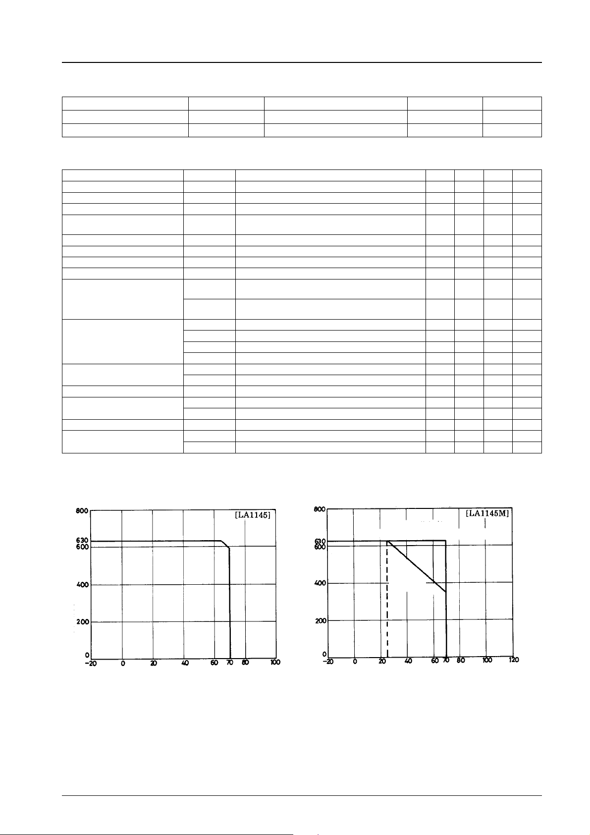
Operating Conditions at Ta = 25°C
Parameter Symbol Conditions Ratings Unit
Recommended supply voltage V
Operating voltage range V
Operating Characteristics at Ta = 25 °C, VCC=8V,fin= 10.7 MHz
Parameter Symbol Conditions min typ max Unit
Quiescent current I
Current drain I
Demodulation output V
Total harmonic distortion THD
Signal-to-noise ratio S/N V
Input limiting voltage V
Muting sensitivity V
Muting bandwidth BW (mute) V
Muting attenuation
Signal strength
indication output
Muting drive output
AM rejection ratio AMR V
Offset voltage
SD sensitivity V
IF count output level
CC
op 7.5to 14 V
CC
CCO
CC
IN
(mute) V16= 2 V 30 36 42 dBµ
IN
mute (1)
mute (2)
V
17-0
V
17-50
V
17-70
V
17-100
V
16-0
V
16-100
V
8-12
V
9-12
SD
V
-On VIN= 100 dBµ, pin 14, CL= 10 pF 110 180 280 mVrms
IF
V
-OFF VIN= 100 dBµ, pin 14, CL=10pF 1 3 mVrms
IF
VIN= 0 dBµ 18 26 36 mA
VIN= 100 dBµ 20 29 40 mA
VIN= 100 dBµ, 400 Hz tone, 100% 300 400 520 mVrms
O
= 100 dBµ, 400 Hz tone, 100%,
V
IN
single tuning coil
= 100 dBµ, 400 Hz tone, 100% 79 85 dB
IN
(lim) 400 Hz tone, 100%, soft mute ON 34 40 46 dBµ
= 100 dBµ, V19% 0.3 V 140 190 280 kHz
IN
V
= 100 dBµ, V16=2V,
IN
400 Hz tone, 100%
= 100 dBµ, V16=4V,
V
IN
400 Hz tone, 100%
VIN= 0 dBµ, R16=10kΩ, pin 17 0 0.1 0.4 V
VIN= 50 dBµ, R16=10kΩ, pin 17 1.4 2.3 3.2 V
VIN= 70 dBµ, R16=10kΩ, pin 17 2.5 4.5 5.5 V
VIN= 100 dBµ, R16=10kΩ, pin 17 5.0 5.5 6.0 V
VIN= 0 dBµ, pin 16 4.0 4.8 5.5 V
VIN= 100 dBµ, pin 16 0 0 0.3 V
= 100 dBµ, 1 kHz tone, 30% AM 57 70 dB
IN
= 0 dBµ, pin 8 to 12 –0.25 0 +0.25 V
V
IN
VIN= 0 dBµ, pin 9 to 12 –0.5 0 +0.5 V
Pin 19 50 58 66 dBµ
8V
0.3 0.8 %
10 15 20 dB
25 29 33 dB
Allowable power dissipation, Pd max – mW
Pdmax–Ta Pdmax–Ta
Ambient temperature, Ta – °C
Allowable power dissipation, Pd max – mW
Mounted on PCB
(90 × 60 × 1.5 mm3glass epoxy
Independent
IC
Ambient temperature, Ta – °C
No. 2725-3/17
Page 4
LA1145, 1145M
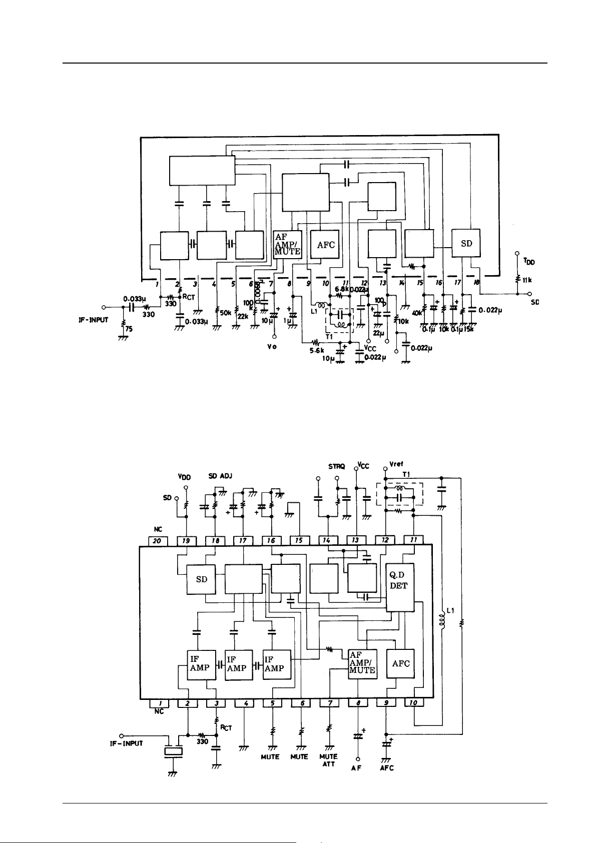
LA1145 Equivalent Circuit Block Diagram
S-meter detector
IF amp
IF amp
IF amp
LA1145M Equivalent Circuit Block Diagram
S-meter Mute
Quadrature
detector
driver
Voltage
regulator
IF
count
Hole
detector/
mute
driver
Unit (resistance: Ω, capacitance: F)
S-meter
detector
Hole
detector/
mute
driver
Start point Gradient
Voltage
regulator
IF
count
*R
is a resistor for variable gain.
CT
Normally 0 Ω.
No. 2725-4/17
Page 5
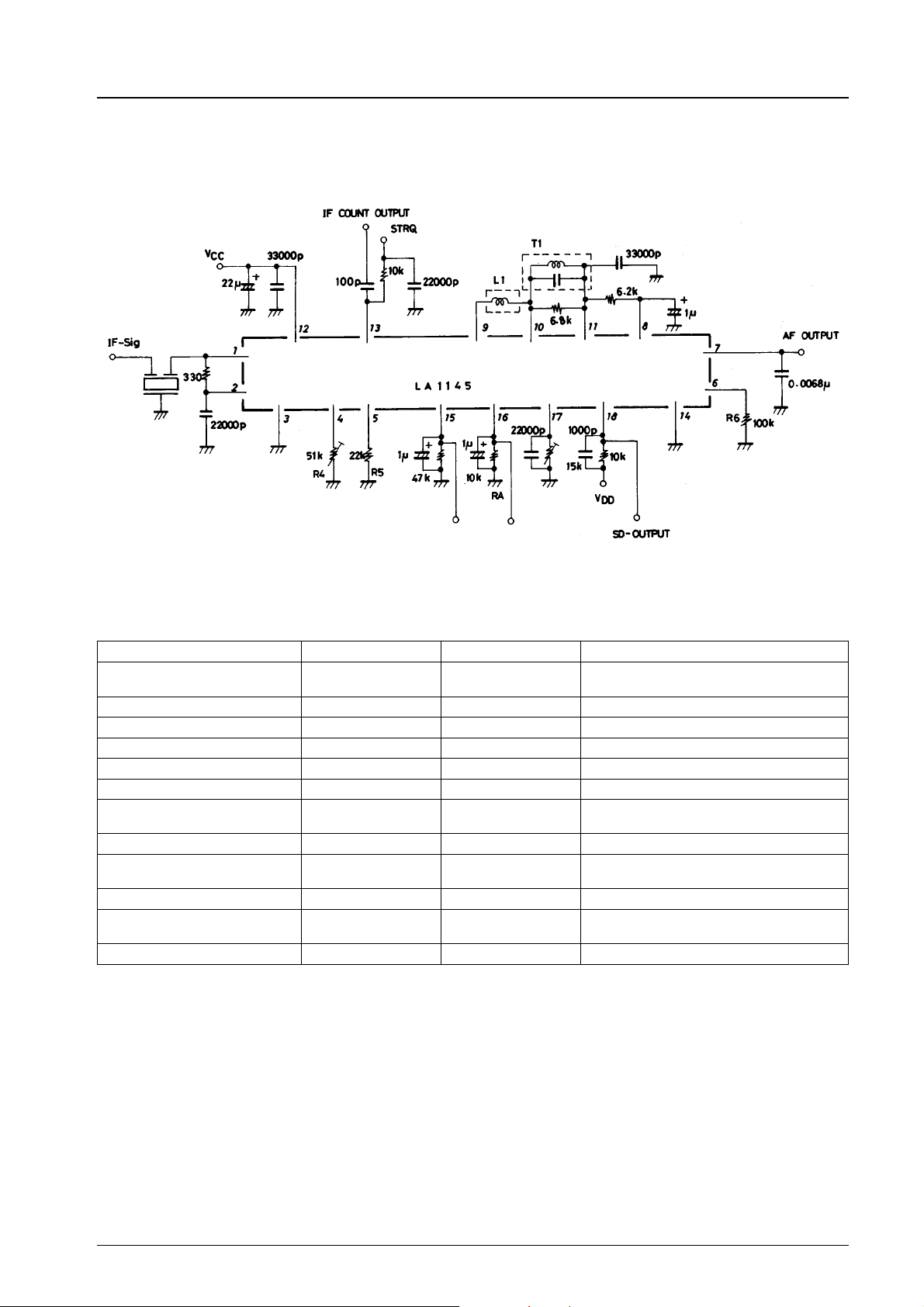
Sample Application Circuit
LA1145, 1145M
50 µs
DC
emphasis
capacitor
Mute driver
output
S-meter
output
Unit (resistance: Ω, capacitance: F)
LS1140 and LS1145 Compared
Parameter LA1140 LA1145 Remarks
Package SIP-16
IF amp, limiter Direct-coupled C-coupled
Quadrature detector jj
AF preamp jj
AFC output jj
Signal meter output j
Band muting j
IF count buffer output – j Common with STRQ
SD circuit – j
S/N 78 dBµ 86 dB
3 dBµ limiting sensitivity 25 dBµ (fixed) 25 to 40 dBµ
Weak signal noise output j
SIP-18Z
MFP-20
j Improved linearity, variable S-meter gradient
C
j
C
j
C
Improved temperature stability,
V
dependent
BE
For the LA1140, Coupled with the soft muting
function.
–3 dBµ limiting sensitivity variable,
independent of soft muting function
L1: 81N-014A (Sumida)
L2: 81N-014B (Sumida)
No. 2725-5/17
Page 6

LA1145, 1145M
LA1145 Pin Description and Typical Voltages
Pin No. Typical Voltage (V) Description Remarks
1 2.6 IF input
2 2.6 IF amp bias
3 0.0 IF amp GND
4 4.0 Mute start control
5 0.2 Mute gradient control
6 2.1 Mute attenuation control
7 4.9 AF output
8 5.0 AFC output
9 4.8 IF output
10 4.8 Quadrature detection input
11 4.8 Voltage regulator output
12 8.0 V
13 0.1 IF count output, control
14 0.0 GND for detection circuit
15 4.8 Mute driver
16 0.2 S-meter output
17 0.2 SD sensitivity control
18 0.1 SD output Open collector
CC
LA1145M Pin Description and Typical Voltages
Pin No. Typical Voltage (V) Description Remarks
1–NC
2 2.6 IF input
3 2.6 IF amp bias
4 0.0 IF amp GND
5 4.0 Mute start control
6 0.2 Mute gradient control
7 2.1 Mute attenuation control
8 4.9 AF output
9 5.0 AFC output
10 4.8 IF output
11 4.8 Quadrature detection input
12 4.8 Voltage regulator output
13 8.0 V
14 0.1 IF count output, control
15 0.0 GND for detection circuit
16 4.8 Mute driver
17 0.2 S-meter output
18 0.2 SD sensitivity control
19 0.1 SD output Open collector
20 – NC
CC
No. 2725-6/17
Page 7
LA1145, 1145M
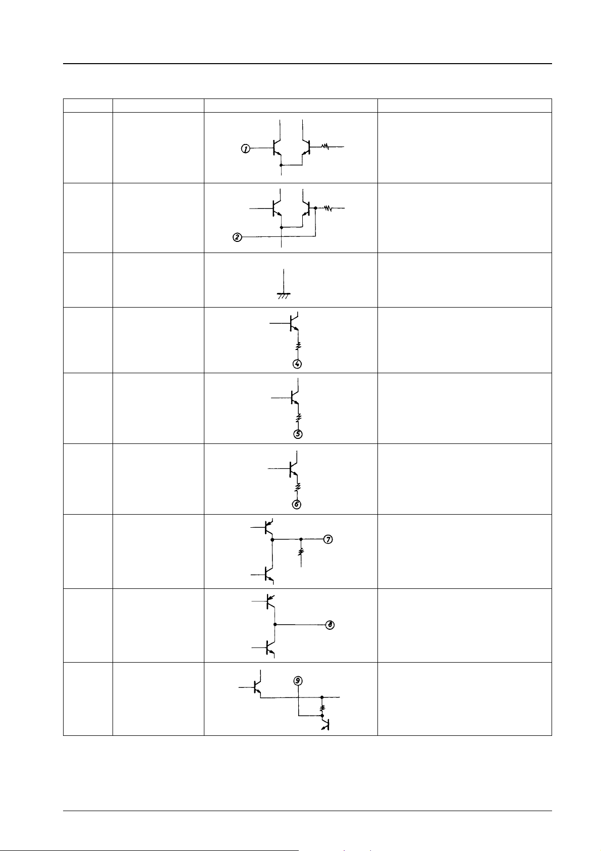
LA1145 Pin Functions (1)
Pin No. Function Internal Equivalent Circuit Notes
1 IF input
2 Bias pin
3 GND
4
5
6 Mute Att
7 FM-AF output
Soft mute start point
control
Soft muting gradient
control pin
IF limiting amp
GND
For setting the soft mute starting point.
Can be used for S-meter output.
For setting the mute gradient from the soft
mute starting point to the noise finishing
point.
For setting amount of mute attenuation.
The demodulation level changes when the
external resistance value is varied.
8 AFC input
9 IF output Output to the phase circuit
No. 2725-7/17
Page 8
LA1145, 1145M
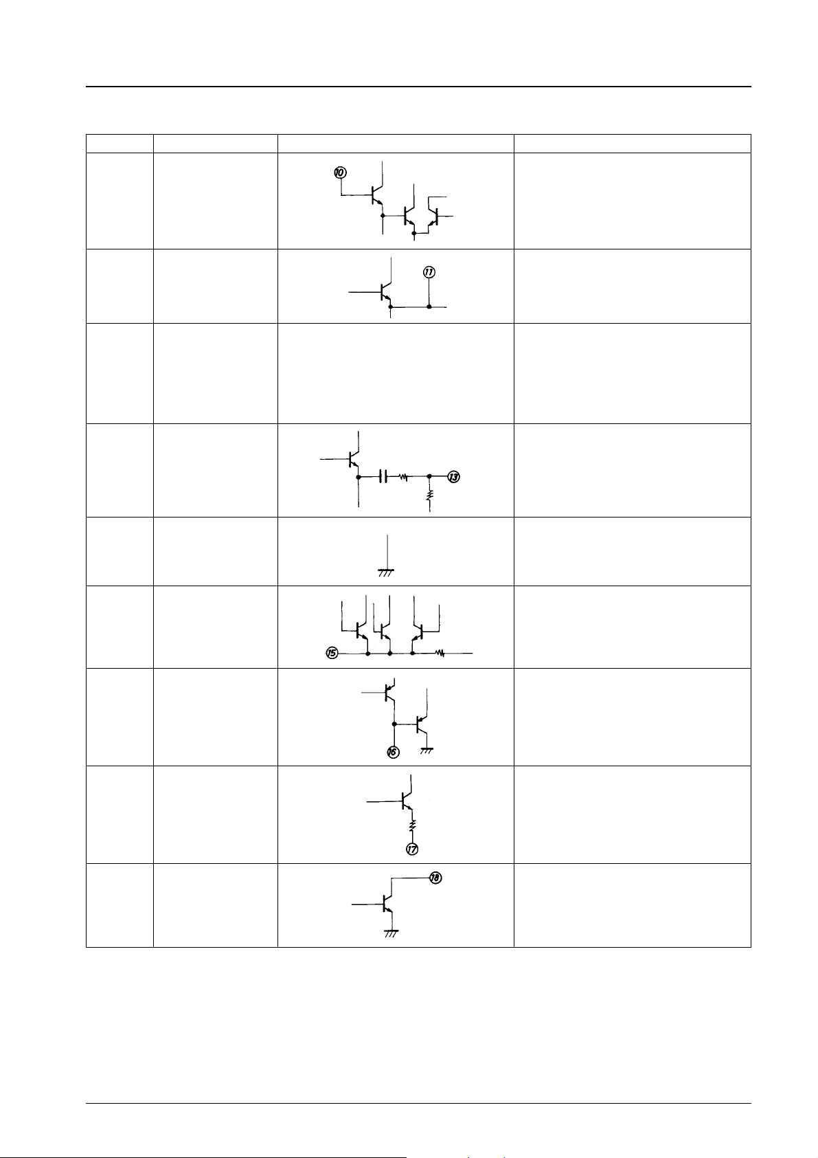
LA1145 Pin Functions (2)
Pin No. Function Internal Equivalent Circuit Notes
IF input via the phase shift circuit. The mute
10 IF input
circuit malfunctions and demodulation output
decreases if the voltage level at this pin
drops below 180 mV.
11 Vref
12 V
13 IF buffer output
14 GND FM detection circuit GND
15 Mute driver
CC
4.8 V
Supply voltage 7.5 to 14 V
Amount of mute attenuation depends on and
is controlled by the voltage at this pin.
16 S-meter output
17 SD sensitivity setting
18 SD output
PNP open collector output
Can be used for S-meter output
High active
No. 2725-8/17
Page 9
LA1145, 1145M
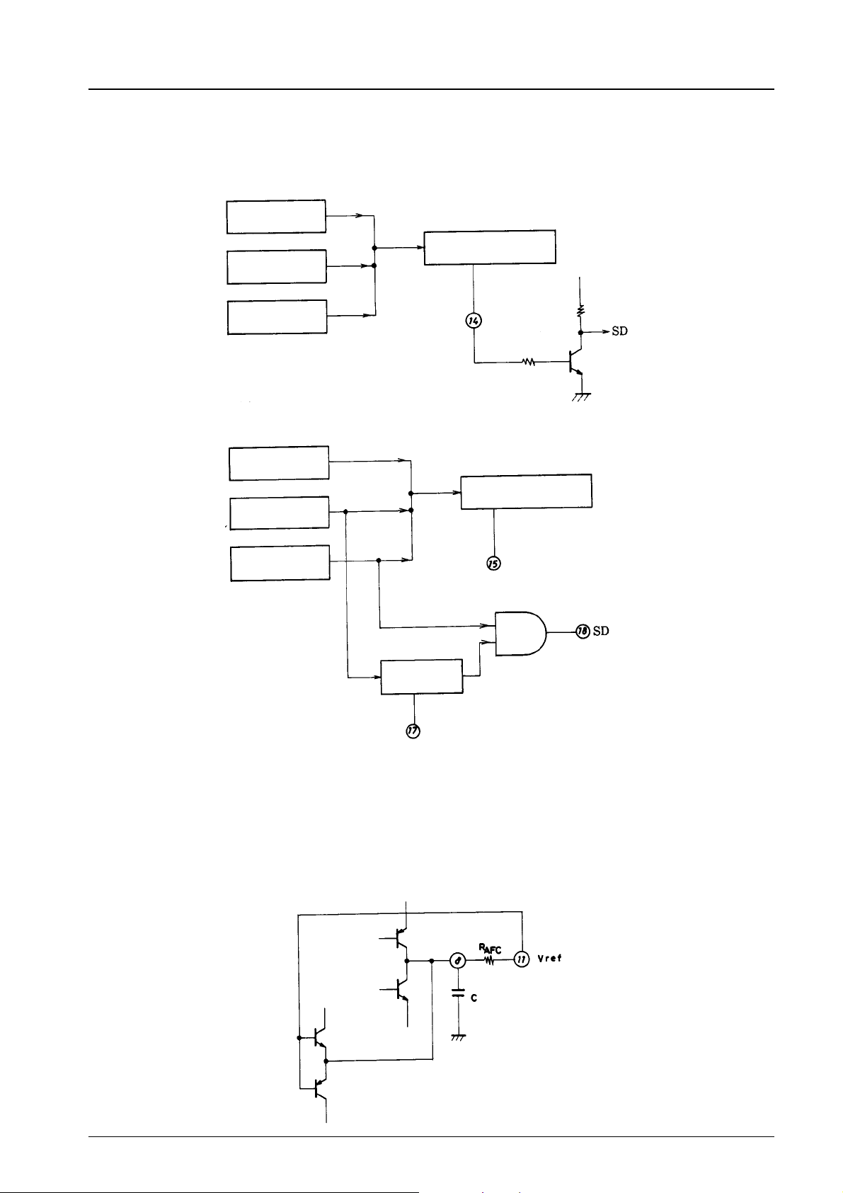
SD Output Circuit
1. LA1145 SD output differs from the LA1140’s pin substitute SD output as shown below. The SD output on the LA1145 does
not operate in conjunction with the soft mute characteristics.
1) LA1140
Hole detector
Mute driver
Signal meter
2) LA1145
Band mute
output
Hole detector
Mute driver
Signal meter
Bandmute
output
Comparator
Exhibit hysteresis
As shown, the SD output is the logical AND of the band mute and S-meter comparator outputs.
2. Signal search using the SD output circuit
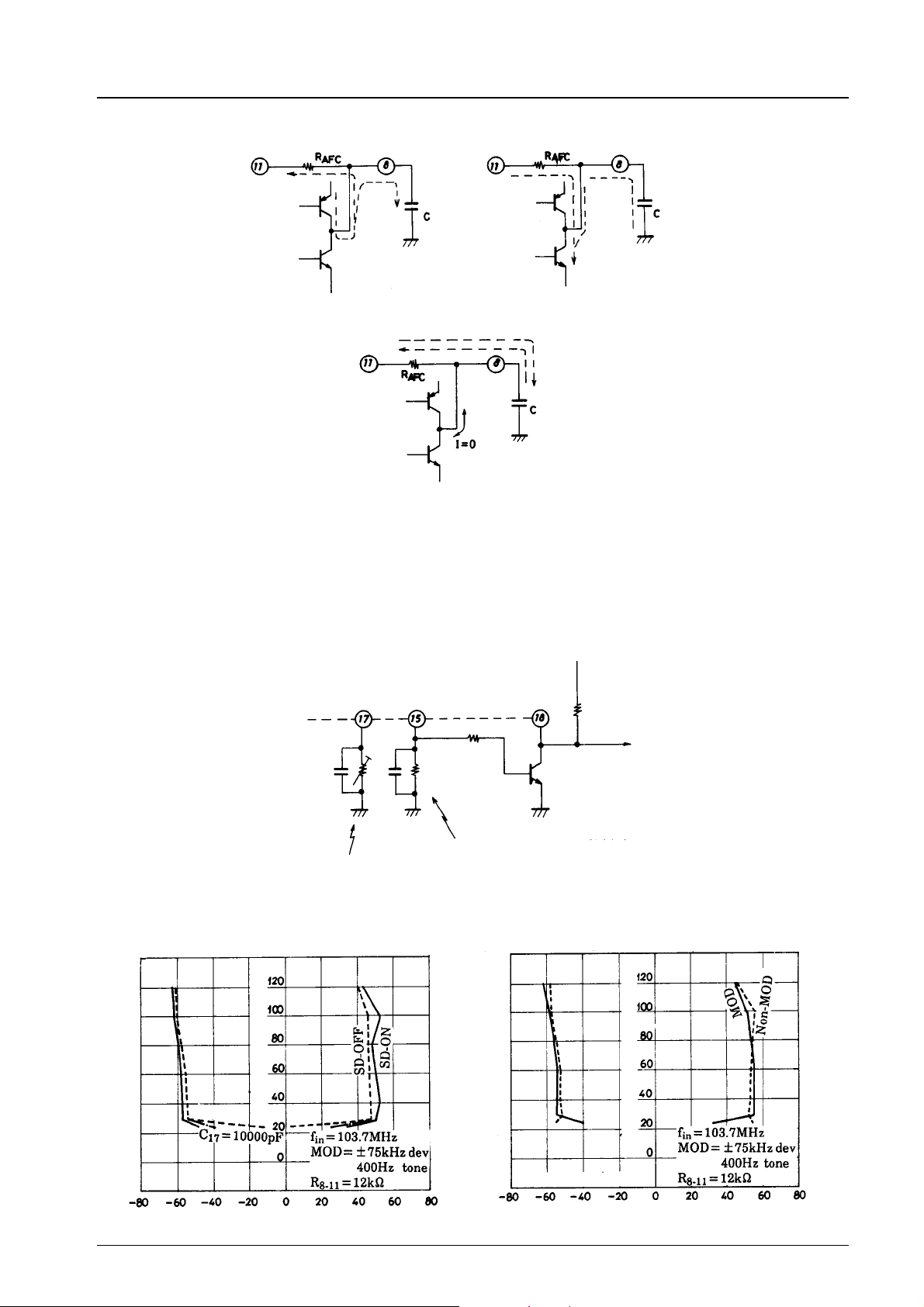
2-1 The transition response characteristics of the SD output circuit depends on the time constants of pins 15, 16, 17 and 8.
As the SD output transition response characteristics are determined by the pin with the largest time constant, erroneous
stopping will result when a search time is less than the largest one.
2-2 Band mute range circuit time constant (pin 8)
An equivalent circuit to the band circuit is shown below.
Mute switch circuit
No. 2725-9/17
Page 10
LA1145, 1145M
1) Current path during detuning
2) Current return path from detuning
The input/output current from pin 8 becomes zero during return.
As can be seen from the above circuit diagrams, the time constant during detuning is determined by the internal PNP
resistance, the NPN collector resistance and the capacitance of the externally- mounted capacitor. This time constant is
determined by the external resistance R
required search time.
and capacitor C. This time constant, τ =R
AFC
× C, must be set depending on the
AFC
3. Narrow-band SD output circuit
An IF count circuit is provided for equipment compatibility for the European marketplace. However, if the band is made
narrow using only the SD circuit, there is a tendency for the number of erroneous stops caused by an undesired signal to
increase. To prevent this, two threshold voltages should be used to control the SD circuit.
SD output
Mute driver pin for the 2nd threshold voltage.
SD sensitivity setting
Band Mute Characteristics (1)
Band Mute Characteristics (2)
ANT input level – dBµ
Without C
17
Frequency, ∆f – kHz
ANT input level – dBµ
With C17= 10000 pF
Frequency, ∆f – kHz
No. 2725-10/17
Page 11
LA1145, 1145M
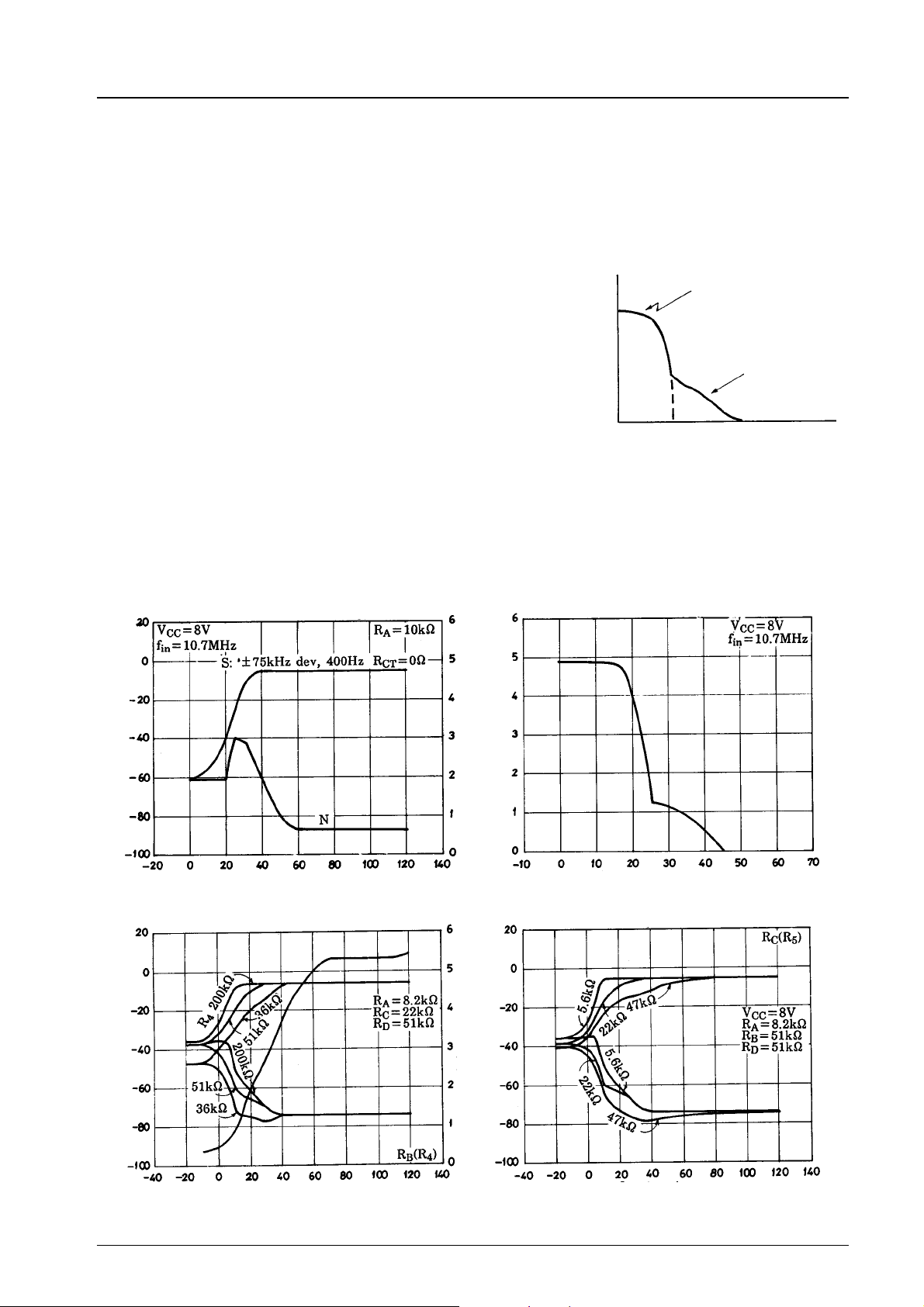
Soft Mute Characteristics
1. Control
The S/N setting (C/N) for weak inputs and the –3 dB limiting sensitivity can be controlled by obtaining the proper value for
the un-soft muted input/output signal characteristic. However, usable sensitivity cannot be controlled as this is determined by
the front end and IF design which are unrelated to soft muting.
2. Soft mute setting
Soft mute operation depends on the S-meter circuit voltage and the hole
detection circuit voltage. As shown in the graph on the right, the degree
of soft muting correlates with the mute drive voltage, V15. The control
signal line of the mute drive voltage switches before and after the
10 dBµ ANT divergence point.
When adjusting the soft mute with a weak signal which does not affect
the S-meter, first adjust it using the hole detection input signal. However,
as the S-meter output will readjust the soft mute level, also adjust the
soft mute using the S-meter output. At this point, the hole detection
output adjusts the gain up to the IF input, causing a variance. Also, the
S-meter output is varied by the value of R
.
16
The LA1145 differs from the LA1140 in that it works with the internal
soft mute circuit continuously engaged.
3. Soft mute transition response characteristic
The degree of soft muting automatically varies according to the change in input field strength. Omitting the influence of the
front end wideband AGC circuit, the LA1145’s response speed is dependent on the time constant at pins 15 and 16.
15
(Mute attenuation)
Mute drive voltage V
Hole detector
S-meter
(Adjust R4, R5)
ANT input level (dBµ)
I/O Characteristics (RCT=0Ω)
Mute Driver Voltage Characteristics
–V
15
S-Meter output voltage – V
Mute driver voltage, V
Demodulation level – dBm/600 Ω
Total harmonic distortion, THD – dB
IF input level, – dBµ
I/O Characteristics (Mute Start Point)
–V
S
I/O Characteristics (Mute Gradient)
IF input level – dBµ
Maximum sensitivity, V
Demodulation level – dBm/600 Ω
ANT input level – dBµ
Demodulation level – dBm/600 Ω
ANT input level – dBµ
No. 2725-11/17
Page 12
LA1145, 1145M
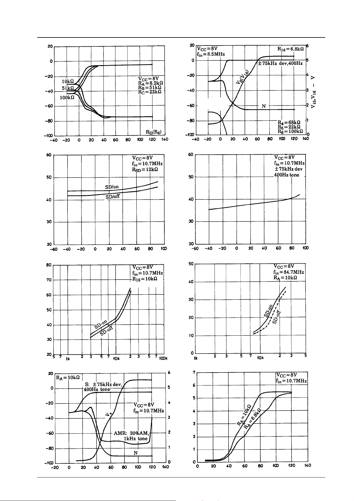
I/O Characteristics (Mute Attenuation Level)
Demodulation level – dBm/600 Ω
ANT input level – dBµ
SD Sensitivity Temperature Characteristics
I/O Characteristics
Mute driver
voltage (V15)
Demodulation level – dB
ANT input level – dBµ
–3 dB Limiting Sensitivity Temperature Characteristics
SD Sensitivity – dBµ
Ambient temperature, Ta – °C
SD Sensitivity Characteristics (IF input)
(S-meter load resistor)
SD sensitivity (IF input level) – dBµ
SD sensitivity resistor value – Ω
I/O Characteristics
–3 dB limiting sensitivity – dBµ
Ambient temperature, Ta – °C
SD Sensitivity Characteristics (ANT input)
SD ON level – dBµ
17RSD-Adj resistor – Ω
S-Meter Characteristics (R
CT
=0Ω)
Output voltage – V
Demodulation level – dBm/600 Ω
Total harmonic distortion, THD – dB
IF input level – dBµ
IF input level – dBµ
No. 2725-12/17
Page 13
LA1145, 1145M
–V
15
Output voltage, V
Attenuation – dB
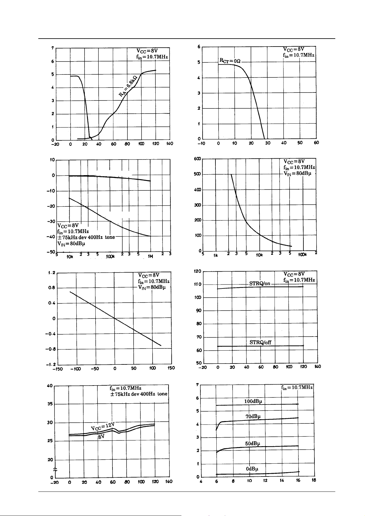
Mute Driver Voltage
IF input level – dBµ
Resistor-Dependent Mute Attenuation
S-level change
Attenuation
Mute Driver Voltage
–V
15
Mute driver voltage, V
IF input level – dBµ
Load Resistance-Dependent Band Muting
Muting range – kHz
Mute driver voltage=4V
Attenuation setting resistor value – Ω
–V
AFC
∆V
Current Drain Characteristics
–mA
CC
AFC Characteristics
Frequency, ∆f – kHz
Muting
Load resistance – Ω
IF Count Output Characteristics
IF count output level – dBµ
IF input level – dBµ
Power Supply-Dependent S-Meter Output Voltage
–V
16
Current drain, I
S-Meter output voltage, V
IF input level – dBµ
Supply voltage, VCC–V
No. 2725-13/17
Page 14
LA1145, 1145M
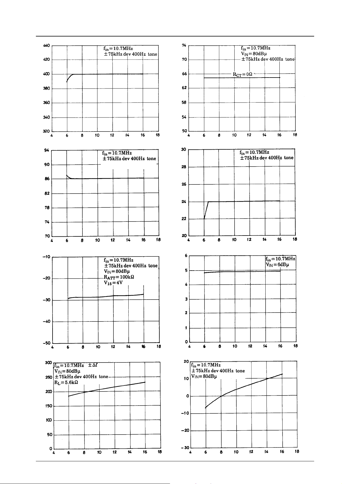
Power Supply-Dependent Demodulation Output
Demodulation output – mVrms
Supply voltage, VCC–V
Power Supply-Dependent S/N
At 2V mute driver voltage
S/N–dB
Power Supply-Dependent AMR
AMR–dB
Supply voltage, VCC–V
Muting Sensitivity Using Hole Detection Output
Supply voltage, VCC–V
Muting Attenuation Characteristics
Attenuation – dB
Supply voltage, VCC–V
Power Supply-Dependent Muting Bandwidth
Muting sensitivity – dBµ
Supply voltage, VCC–V
Power Supply-Dependent Mute Driver Voltage
Mute driver voltage – V
Supply voltage, VCC–V
Tuning Point Shift
Muting bandwidth – kHz
Supply voltage, VCC–V
Tuning drift, ∆f – kHz
Supply voltage, VCC–V
No. 2725-14/17
Page 15
LA1145, 1145M
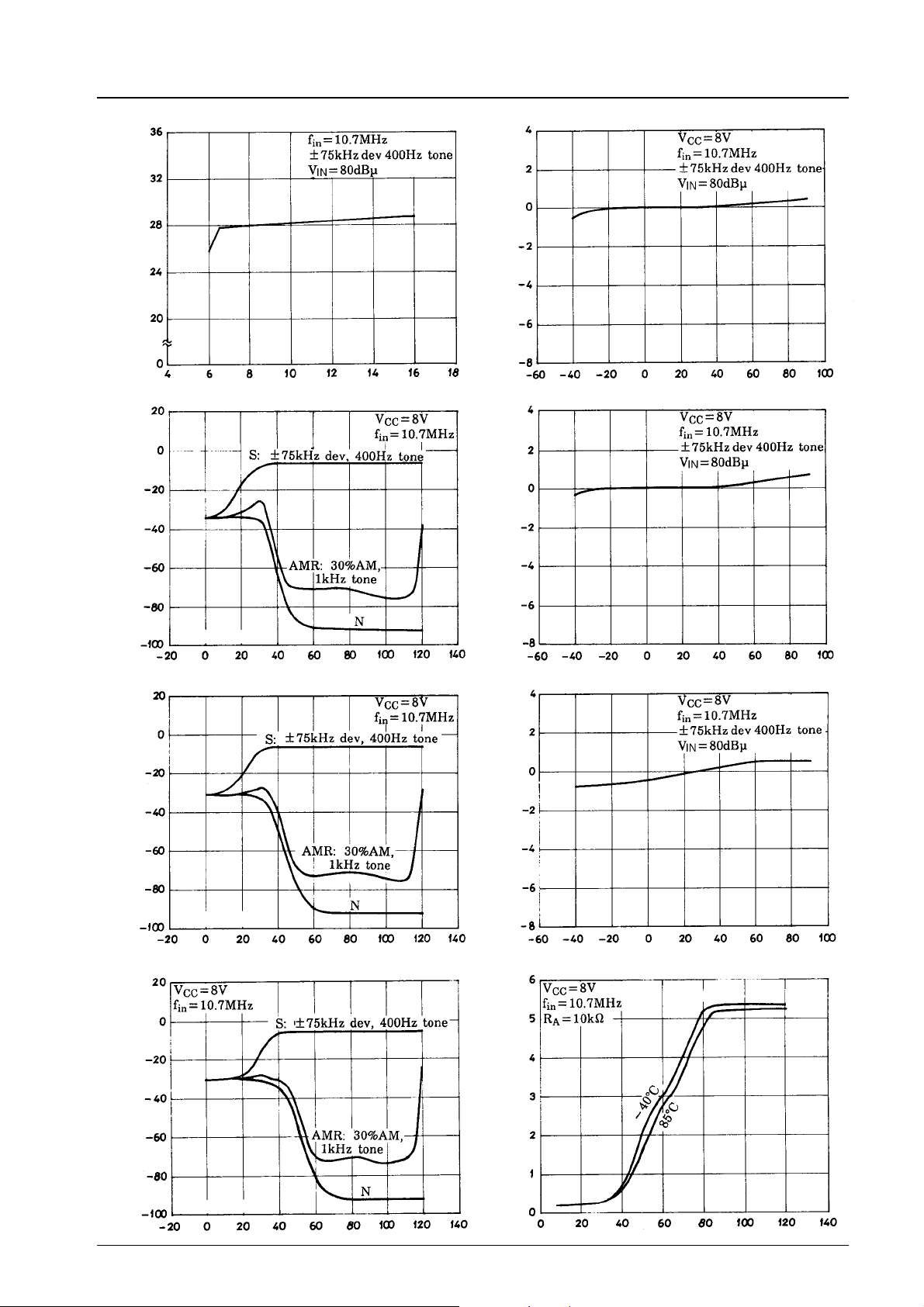
–mA
Current drain, I
CC
Current Drain Characteristics
Supply voltage, VCC–V
I/O Characteristics (RCT=0Ω)
I/O Characteristic (R
CT
=0Ω)
Demodulation level shift – dB
Ambient temperature, Ta – °C
I/O Characteristics (R
= 100 Ω)
CT
Demodulation output – dBm/600 Ω
Demodulation output – dBm/600 Ω
Pin 15 short
IF input level – dBµ
I/O Characteristics (RCT= 100 Ω)
Pin 15 short
IF input level – dBµ
I/O Characteristics (RCT= 510 Ω)
Demodulation level shift – dB
Ambient temperature, Ta – °C
I/O Characteristics (R
= 510 Ω)
CT
Demodulation level shift – dB
Ambient temperature, Ta – °C
S-Meter Characteristics (Temperature Characteristic)
Demodulation output – dBm/600 Ω
Pin 15 short
IF input level – dBµ
S-Meter output voltage – V
IF input level – dBµ
No. 2725-15/17
Page 16
LA1145, 1145M
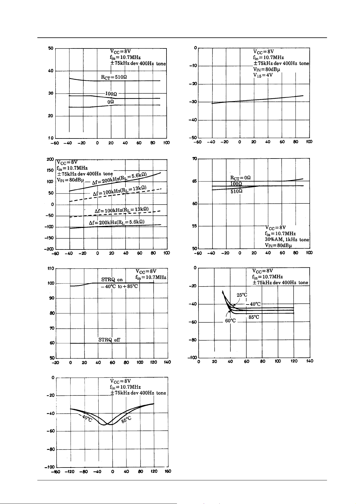
–3 dB Limiting Sensitivity Temperature Characteristics
–3 dB limiting sensitivity – dBµ
Pin 15 short
Ambient temperature, Ta – °C
Muting Bandwidth Temperature Characteristics
Muting Attenuation Characteristics
Muting attenuation – dB
Ambient temperature, Ta – °C
AMR Temperature Characteristics
AMR–dB
Muting bandwidth – kHz
IF count output level – dBµ
Ambient temperature, Ta – °C
IF Count Output Level Shift
IF input level – dBµ
THD Detuning Characteristics
Ambient temperature, Ta – °C
THD Characteristic (Single Tuning Circuit)
∆V
=0V
Total harmonic distortion, THD – dB
AFC
IF input level – dBµ
∆V
Total harmonic distortion, THD – dB
AFC
=0V
Detuning frequency – kHz
No. 2725-16/17
Page 17

LA1145, 1145M
No products described or contained herein are intended for use in surgical implants, life-support systems,
aerospace equipment, nuclear power control systems, vehicles, disaster/crime-prevention equipment and the like,
the failure of which may directly or indirectly cause injury, death or property loss.
Anyone purchasing any products described or contained herein for an above-mentioned use shall:
1 Accept full responsibility and indemnify and defend SANYO ELECTRIC CO., LTD., its affiliates,subsidiaries and
distributors and all their officers and employees, jointly and severally, against any and all claims and litigation
and all damages, cost and expenses associated with such use:
2 Not impose any responsibility for any fault or negligence which may be cited in any such claim or litigation on
SANYO ELECTRIC CO., LTD., its affiliates, subsidiaries and distributors or any of their officers and employees
jointly or severally.
Information (including circuit diagrams and circuit parameters) herein is for example only; it is not guaranteed for
volume production. SANYO believes information herein is accurate and reliable, but no guarantees are made or
implied regarding its use or any infringements of intellectual property rights or other rights of third parties.
This catalog provides information as of September,1997. Specifications and information herein are subject to change without notice.
No. 2725-17/17
 Loading...