

Page 1
HALFBRIDGE OUTPUTS WITH TYPICAL
R
= 0.7Ω
ON
OUTPUTCURRENT CAPABILITY±1.2A
OPERATING SUPPLY VOLTAGE RANGE 7V
TO 16.5V
SUPPLY OVERVOLTAGE PROTECTION
FUNCTIONFOR V
UP TO 40V
VS
VERY LOW QUIESCENT CURRENT IN
STANDBYMODE < 1µA
CMOS COMPATIBLE INPUTS WITH HYSTERESIS
OUTPUTSHORT-CIRCUIT PROTECTION
THERMALSHUTDOWN
REAL TIME DIAGNOSTIC: THERMAL OVER-
LOAD, OVERVOLTAGE
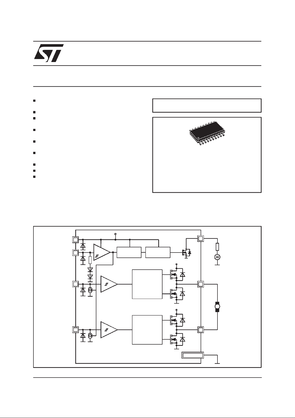
L9997ND
DUAL HALF BRIDGE DRIVER
MULTIPOWER BCD TECHNOLOGY
SO20 (12+4+4)
ORDERING NUMBERS:
L9997ND
L9997ND013TR
DESCRIPTION
The L9997ND is a monolithic integrated driver, in
BCD technology intended to drive various loads,
BLOCK DIAGRAM
VS VS
1
EN
IN1
IN2
10
12
9
ENABLE
REFERENCE
BIAS
including DC motors. The circuit is optimized for
automotiveelectronicsenviromental conditions.
DIAG
11
PROTECTION
FUNCTIONS
DRIVER 1
DRIVER 2
VS
OUT1
19
VS
OUT2
2
5V
M
April 1999
GND
4...7,1 4...17
1/9
Page 2
L9997ND
ABSOLUTE MAXIMUM RATINGS
Symbol Parameter Value Unit
V
V
V
V
I
VSDC
VSP
I
OUT
IN1,2
V
EN
DIAG
I
OUT
DIAG
DC Supply Voltage -0.3 to 26 V
Supply VoltagePulse (T < 400ms) 40 V
DC Output Current ±1.8 A
DC Input Voltage -0.3 to 7 V
Enable Input Voltage -0.3 to 7 V
DC Output Voltage -0.3 to 7 V
DC Output Short-circuit Current -0.3V < V
OUT<VS
+ 0.3V internally limited
DC Sink Current -0.3V< VDG< 7V internally limited
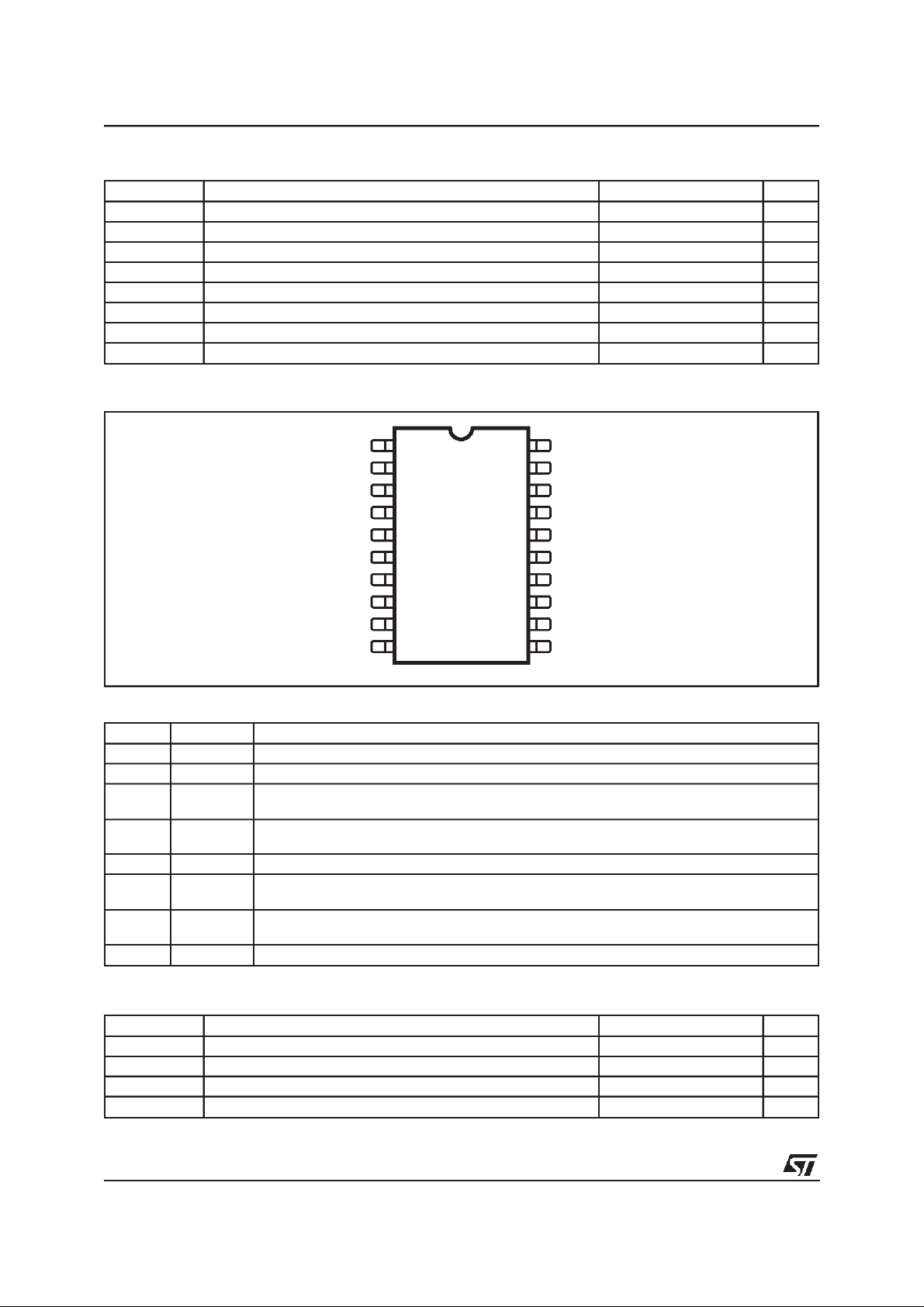
PIN CONNECTION
(Topview)
V
S
OUT2
N.C.
GND
GND
GND
GND
N.C.
IN2 IN1
EN DIAG
2
3
4
5
6
7
8
9
10
D95AT166
20
19
18
17
16
15
14
13
12
11
N.C.1
OUT1
N.C.
GND
GND
GND
GND
N.C.
PIN FUNCTIONS
N. Name Function
1 VS Supply Voltage
2 OUT2 Channel 2: Push-Pull power output with intrinsic body diode
3, 8, 13,
18,20
4to7,
14 to 17
9 IN2 Input 2: Schmitt Trigger input with hysteresis(non-inverting signalcontrol)
10 EN Enable: LOW or not connected on thisinput switchesthe device into standby mode andthe
11 DIAG Diagnostic: Open Drain Output thatswitches LOW if overvoltage or overtemperature is
12 IN1 Input 1: Schmitt Trigger input with hysteresis(non-inverting signalcontrol)
NC NC: Not Connected
GND Ground: signal - and power - ground, heat sink
outputs into tristate
detected
THERMAL DATA
Symbol Parameter Value Unit
T
jTS
T
jTSH
R
th j-amb
R
th j-pins
(1) With6cm2on board heatsink area.
2/9
Thermal Shut-down Junction Temperature 165 °C
Thermal Shut-down Threshold Hysteresis 25 K
Thermal Resistance Junction-Ambient
(1)
50 K/W
Thermal Resistance Junction-Pins 15 K/W
Page 3
L9997ND
ELECTRICALCHARACTERISTICS (7V < VS< 16.5V;-40°C< TJ< 150°C;unlessotherwisespecified.)
Symbol Parameter Test Condition Min. Typ. Max. Unit
I
VS_SB
I
VS
V
ENL
V
ENH
V
ENthh
I
EN
V
IN1,2L
V
IN1,2H
V
IN1,2thh
I
IN1,2
R
ON OUT1,2
|I
OUT1,2
V
DIAG
V
VSOVth
t
ONLH
t
ONHL
t
OFFHL
t
OFFLH
t
dHL
t
dLH
t
rHS
t
rLS
t
fHS
t
fLS
* Tested at 125°C and guaranteedby correlation
Quiescent Currentin Standby
Mode
Supply Current EN = HIGH, I
VEN< 0.3V;VVS<16.5V;Tj< 85°(*)
V
=0; VVS= 14.5V; Tj =25°C
EN
=0 2 6 mA
OUT1,2
<1
<1
90
10
µA
µA
Low Enable Voltage 1.5 V
High Enable Voltage 3.5 6 V
Enable Threshold Hysteresis 1 V
Enable Input Current VEN= 5V 85 250 µA
Low Input Voltage 1.5 V
High Input Voltage 3.5 V
Input Threshold Hysteresis 1 V
Input Bias Current VIN=0
V
= 5V, EN = HIGH
IN
ON-Resistance to Supply or
GND
I
= ±0.8A; VVS= 7V; Tj= 125°C
OUT
I
= ±0.8A;VVS=12V;Tj= 125°C
OUT
I
= ±0.8A; VVS= 12V; Tj=25°C
OUT
-3
2
0
10
1.2
1.1
1
50
2.8
2.25
µA
µA
0.7
| Output CurrentLimitation 1.2 1.6 2.2 A
Diagnostic OutputDrop I
= 0.5mA, EN = HIGH
DIAG
0.6 V
Overvoltage orThermal Shutdown
Supply Overvoltage
17 19 21 V
Threshold
Turn on Delay Time See Fig. 2; VVS= 13.5V
Measured with 93Ωload
50 150 µs
30 150 µs
Turn off Delay Time 10 100
220µs
Rising Delay Time 115 250
Falling Delay Time 115 250 µs
Rise Time 30 100
60 150 µs
Fall Time 25 100
50 150 µs
Ω
Ω
Ω
s
µ
s
µ
s
µ
s
µ
FUNCTIONAL DESCRIPTION
The L9997ND is a motor driver two half-bridge
outputs, intended for driving dc motorsin automotive systems. The basic function of the device is
shownin the Table1.
Table 1. Table function.
Status EN IN1 IN2 OUT1 OUT2 DIAG NOTE
1 L X X Tristate Tristate OFF Standby Mode
2 H H H SRC SRC OFF Recommended for braking
3 H H L SRC SNK OFF
4 H L H SNK SRC OFF
5 H L L SNK SNK OFF
6 H X X Tristate Tristate ON Overvoltage or Overtemperature
3/9
Page 4

L9997ND
The device is activated with enable input voltage
HIGH. For enable input floating (not connected)
or LOW the device is in Standby Mode. Very low
quiescentcurrent is defined for V
< 0.3V. When
EN
activating or disactivating the device by the enable input a wake-up time of 50µs is recommended.
For braking of the motor the status 2 is recommended. The reason for this recommendation is
that the device features higher threshold for initialisation of parasiticstructuresthan in state 5.
The inputs IN1, IN2 features internal sink current
generators of 10µA, disabled in standby mode.
With these input currentgeneratorsthe input level
is forced to LOW for inputsopen. In this condition
the outputs are in SNK state.
The circuit features an overvoltage disable function referred to the supply voltage V
. Thisfunc-
VS
tion assures disabling the power outputs, when
the supply voltage exceeds the over voltage
threshold value of 19V typ. Both outputs are
forced to tristateinthis conditionand the diagnostic output is ON.
The thermal shut-down disables the outputs(tristate) and activates the diagnostic when the junction temperature increases above the thermal
shut-down threshold temperature of min. 150°C.
For the start of a heavyloaded motor, if the motor
current reaches the max. value, it is necessary to
respect the dynamical thermal resistance junction
to ambient.The outputs OUT1 and OUT2are protected against short circuit to GND or V
, for sup-
S
ply voltagesup to the overvoltagedisable threshold.
The output power DMOS transistors works in linear mode for an output current less than 1.2A. Increasing the output load current (> 1.2A) the out-
put transistor changes in the current regulation
mode, see Fig.6, with the typical output current
value below 2A. The SRC output power DMOS
transistorsrequires a voltagedrop ~3V to activate
the current regulation. Below this voltage drop is
the device also protected.The output current heat
up the power DMOS transistor, the R
DSON
increases with the junction temperature and decreases the output current. The power dissipation
in this condition can activate the thermal shutdown . In the case of output disable due to thermal overload the output remains disabled untill
the junction temperature decreases under the
thermalenable threshold.
Permanent short circuit condition with power dissipation leading tochip overheatingand activation
of the thermal shut-down leads to the thermaloscillation. The junction temperature difference between the switch ON and OFF points is the thermal hysteresis of the thermal protection. This
hysteresis together with the thermal impedance
and ambient temperature determines the frequency of this thermal oscillation, its typical values are in therange of 10kHz.
The open drain diagnostic output needs an external pull-up resistor to a 5V supply. In systems
with several L9997ND the diagnostic outputs can
be connected together with a common pull-up resistor. The DIAG output current is internally limited.
Fig. 1 shows a typical application diagram for the
DC motor driving. To assurethe safety of the circuit in the reversebattery conditiona reverse protection diode D
tection diode D
supply voltage V
line will be limited to a value lower than the
V
BAT
absolute maximum rating for V
is necessary. The transient pro-
1
must assure that the maximal
2
during the transients at the
VS
.
VS
Figure 1: ApplicationCircuitDiagram.
5V
CONTROL
LOGIC
4/9
Ω
47K
IDIAG1
IIN1
IIN2
IEN
DIAG1
IN1
IN2
EN
S
V
L9997ND
GND
Is
S
C
OUT1
IOUT1
OUT2
IOUT2
D1
VBAT
2
D
IM
VM
M
GND
Page 5

Figure 2. Timing Diagram.
L9997ND
Standby Mode Operating Mode Overtemperature
EN
IN1
IN2
DIAG
OUT1
OUT2
Tristate
Tristate
t
10%
dLH
90%
t
r
t
dHL
t
t
ONHL
t
ONLH
90%
50%
10%
t
rf
t
dHL
t
f
t
dLH
or Overvoltage
t
dLH
Tristate
t
dHL
Tristate
t
t
dHL
dLH
Standby Mode
t
OFFLH
Tristate
t
OFFHL
Tristate
Figure 3. Typical R
- Characteristicsof Source and Sink Stage
ON
5/9
Page 6

L9997ND
Figure 4. Quiescentcurrent in standbymode versus supply voltage.
Figure 5. ON-Resistanceversus supply voltage.
6/9
Page 7

L9997ND
Figure 6. I
OUT
versusV
(pulsedmeasurementwith TON= 500µs, T
OUT
= 500ms).
OFF
Figure 7. Test circuit.
12V
V
EN
V
IN1
100µF
V
IN2
200nF
EN
IN1
IN2
VS
L9997ND
GND
DIAG
OUT1
OUT2
10kΩ
15
15
5V
Ω
Ω
7/9
Page 8

L9997ND
8/9
Page 9

L9997ND
Information furnished is believed to be accurate and reliable. However, STMicroelectronics assumes no responsibility for the consequences
of use of such information nor for any infringement of patents or other rights of third parties which may result from its use. No license is
granted by implication or otherwise under any patent or patent rights of STMicroelectronics. Specification mentioned in this publication are
subject to change without notice. This publicationsupersedes and replaces all information previously supplied. STMicroelectronics products
are not authorized for use as criticalcomponents in life support devices or systems without express written approval of STMicroelectronics.
The ST logo is a registered trademark of STMicroelectronics
1999 STMicroelectronics – Printed in Italy – AllRights Reserved
STMicroelectronics GROUP OF COMPANIES
Australia - Brazil - Canada- China- France - Germany - Italy - Japan - Korea- Malaysia - Malta- Mexico - Morocco - The Netherlands -
Singapore - Spain - Sweden - Switzerland- Taiwan- Thailand - United Kingdom - U.S.A.
http://www.st.com
9/9
 Loading...