

Page 1
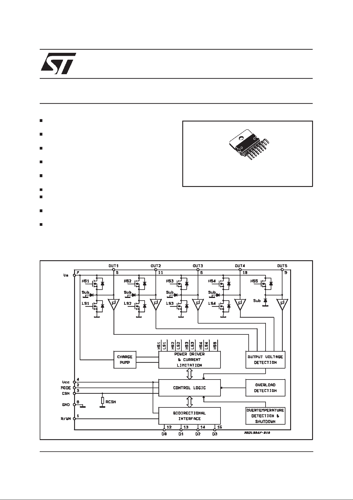
QUAD HALF-BRIDGEAND SINGLE HIGH-SIDE DRIVER
LOW CONSUMPTION IN STANDBY MODE
(<100µA AT ROM TEMP; < 150µA AT130°C)
TWOHALFBRIDGESFOR3ALOAD
(R
TWOHALFBRIDGESFOR0.5ALOAD
(R
HIGHSIDE DRIVER FOR 2.5ALOAD
(R
DIRECT CONTROLLED BYµC (MULTIPLEX
SYSTEM)
OUTPUTHIGH/LOW LEVELDIAGNOSTIC
OVERCURRENT SWITCH OFF AND DIAG-
NOSTIC
OVERTEMPERATURE DIAGNOSTIC BE-
FORE SWITCH OFF
OPENLOAD DIAGNOSTIC
DESCRIPTION
The L9947 is a bus controlled power interface in-
=0.25Ω TYP;Tj=25°C)
DSON
=2.5Ω TYP;Tj=25°C)
DSON
=0.45Ω TYP; Tj=25°C)
DSON
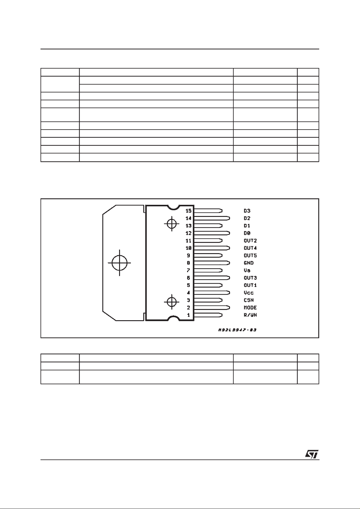
L9947
Multiwatt 15
ORDERING NUMBER:
tended for automotive applications realized in
multipower BCD60II technology. Up to three DC
motors and one grounded resistive load can be
driven with its four half-bridge and one high-side
driverpower outputs. The microcomputer compatible bidirectional parallel bus allows several interfaces connected on the same bus (multiplex system). The full diagnosticinformation is available on
thebus.
L9947S
BLOCK DIAGRAM
April 1999
1/13
Page 2
L9947
ABSOLUTE MAXIMUM RATINGS
Symbol Parameter Value Unit
V
S
I
S
V
CC
V
CSN,VR/WN
V
MODE
V
D0 -D3
I
OUT1 - OUT5
T
j
T
j-SD
T
j-HYS
PIN CONNECTION
DC Supply Voltage 26 V
Single Pulse t
< 400ms 40 V
max
Negative Supply Current -9 A
Stabilized Supply Voltage -0.3 to 6V V
Digital Input Voltage -0.3 to VCC+0.3 V
Digital Input/ Output Voltage -0.3 to VCC+0.3 V
Output Current Power internal limited
Operating Junction Temperature -40 to 150
Thermal ShutdownJunction Temperature min 150
Thermal JunctionTemperature Hysteresis 20 K
C
°
C
°
THERMAL DATA
Symbol Parameter Value Unit
2/13
R
th j-amb
Z
th j-amb
Thermal ResistanceJunction AmbientP
Thermal ResistanceJunction Ambientstill air;
single pulse tp=20s
= 25W; free air; DC 38 °C/W
tot
10 °C/W
Page 3
L9947
ELECTRICAL CHARACTERISTICS
= 8 to 16V; VCC= 4.5 to 5.5V; Tj= -40 to 150°C;unless other-
(V
S
wise specified; the voltage are refered to GND and currents are assumed positive, when the current
flows into the pin.)
SUPPLY:
Symbol Parameter Test Condition Min. Typ. Max. Unit
CC DC Supply Current V
I
= 16V; VCC= 5.5V; (status
S
5mA
8)
I
S
DC Supply Current VS= 16V; VCC= 5.5V; (status
10 mA
8)
I
CC + I
Sum Supply Current I
S
OUT1=IOUT2=IOUT3=IOUT4 =
I
= 0; Standby (status 2)V
OUT5
S
100 µA
= 14V; VCC= 5.5V;
T
= -40 to 25°C
j
I
OUT1=IOUT2=IOUT3=IOUT4 =
I
= 0; Standby (status 2)V
OUT5
S
150 µA
= 14V; VCC= 5.5V;
T
>25°C
j
< 14V; VCC= 5.5V; I
V
S
OUT
=0;
3mA
(status 17);
V
SOVT
Overvoltage Shutdown
17 25 V
Threshold
CONTROLINPUTS: CNS, R/WN, MODE
Symbol Parameter Test Condition Min. Typ. Max. Unit
V
V
V
INL
INH
INHyst
I
INL
I
INH
Input Low Level VCC= 5V 1.5 V
Input High Level VCC= 5V 3.5 V
Input Hysteresis VCC= 5V; 0.5 V
Input Current Low VCC= 5V; VIN= 0 -10 10 µA
Input Current High (with
VCC= 5V; VIN= 5V -10 10 µA
exception of CSN Input)
R
CSN
Input Resistance to GND (pull
20 KΩ
down at CSN pin)
DATA INPUT: D0 - D3
Symbol Parameter Test Condition Min. Typ. Max. Unit
V
V
V
DINHyst
I
DINL
I
DINH
DINL
DINH
Input Low Level VCC= 5V; MODE = 0 1.5 V
Input High Level VCC= 5V; MODE = 0 3.5 V
Input Hysteresis VCC= 5V; MODE = 0 0.5 V
Input Current Low VCC= 5V; VIN= 0 -10 10 µA
Input Current High VCC= 5V; VIN= 5V -10 10 µA
DATA OUTPUT:D0 - D3
Symbol Parameter Test Condition Min. Typ. Max. Unit
V
V
DOL
DINH
Output Low Level VCC= 5V; ID= 0.5mA; MODE
=1
Input High Level VCC= 5V; ID= 0.5mA; MODE
=1
4V
0.6 V
3/13
Page 4
L9947
ELECTRICALCHARACTERISTICS
(continued)
OUTPUTS:
Symbol Parameter Test Condition Min. Typ. Max. Unit
R
ON OUT1
On Resistance to Supplyor
GND
R
ON OUT2
On Resistance to Supplyor
GND
R
ON OUT3
On Resistance to Supplyor
GND
R
ON OUT4
On Resistance to Supplyor
GND
R
ON OUT5
|I
OUT1
On Resistance to Supply VS=8V; Tj= 125°C; I
| Output Current Limitation to
Supply or GND
|I
| Output Current Limitation to
OUT2
Supply or GND
|I
| Output Current Limitation to
OUT3
Supply or GND
|I
| Output Current Limitation to
OUT4
Supply or GND
|I
| OutputCurrentLimitation to GND 2.5 7.5 A
OUT5
I
OUT1
I
OUtT2
I
OUT3
I
OUT4
I
OUT5
V
OUT1-5
Output Current V
Output Current V
Output Current V
Output Current V
Output Current V
Output Voltage Detection
Thresholds
T
JOT
Overtemperature Detection
Thresholds
t
f
OSC
ISC
Overcurrent Switch off Time 50
Internal Oscillator Frequency 250 KHz
VS=8V; Tj= 125°C;
I
= ±0.5A
OUT
>10V; Tj =125°C;
V
S
I
=± 0.5A
OUT
VS=8V; Tj= 125°C;
I
= ±0.5A
OUT
> 10V; Tj=125°C;
V
S
I
=± 0.5A
OUT
VS=8V; Tj= 125°C;
I
= ±2.5A
OUT
> 10V; Tj=125°C;
V
S
I
=± 2.5A
OUT
VS=8V; Tj= 125°C;
I
= ±2.5A
OUT
>10V; Tj=125°C;
V
S
I
=± 2.5A
OUT
= -2A 1.0 Ω
OUT
> 10V; Tj=125°C;
V
S
I
= -2A
OUT
For the function of the short
0.67 2 A
6 Ω
3.95 Ω
6 Ω
3.95 Ω
600 mΩ
395 mΩ
600 mΩ
395 mΩ
0.7 Ω
circuit current limitation see the
functional description (pag....)
0.67 2 A
412A
412A
=2.5V;(status 18) 5 15 mA
OUT1
=2.5V;(status 18) 5 15 mA
OUT2
=2.5V;(status 18) 5 15 mA
OUT3
=2.5V;(status 17) 80 500 mA
OUT4
V
OUT4=VS
OUT5=VS
-2.5V;(status 16 or 18) -80 -500 mA
-2.5V;(status 18) -5 -15 mA
VS=13V; (status 11)
4.9
LOW
HIGH
HYSTERESIS
7.5
0.4 V
0.6 V
0.2 V
5.5
S
8.1
S
S
status 12 - 15 130 °C
steady state t >20ms 125 <T
JSD
°C
µ
V
V
V
s
4/13
Page 5

APPLICATIONCIRCUIT DIAGRAM
Fogure 1: RecommendedApplication Circuit.
L9947
FUNCTIONAL DESCRIPTION
The L9947 is a power interface circuit designed
for a multiplex system controlled by a parallel µC
bus. The bus consists of four bidirectional data
wires D0 - D3 and three control wires read/write
(R/WN), mode (MODE) and chip select (CSN).
The device needs two supply voltages. The first
voltage supplies the half bridges, high side driver
and its driving part. The second one is a 5V stabilizedsupply. The functionof thedevice in thetypical operating modes is described in the following
tables.
5/13
Page 6

L9947
Output Activating/writeTable 1
Status CSN R/WN MODE D0 D1 D2 D3 OUT1 OUT2 OUT3 OUT4 OUT5 FUNCTION
1 1 X X X X X X AB AB AB AB AB Hold output behavious as
2 _ 0 0 0 0 0 0 T T T T T AllOutputs,Standbymode
3 _ 0 0 0 0 1 0 SRC T T SNK T M1, right
4 _ 0 0 1 1 0 0 SNK T T SRC T M1, left
5
_
6
_
7 _ 0 0 0 1 1 0 T T SRC SNK T M3, right
8 _ 0 0 1 0 0 0 T T SNK SRC T M3, left
9 _ 0 0 1 1 1 0 SNK SNK SNK SNK T Braking
10
_
0 0 1 0 1 0 T SRC T SNK T M2, right
0 0 0 1 0 0 T SNK T SRC T M2, left
0 0 0 0 0 1 T T T T SRC High side driver
Notes:
Where CSN = 0 the device is (for t≤100µs) transparent, in this condition any changeof Data D0 .... D3
will lead to the apprpriateoutput response.
Deselectingthe circuit(CSN ) the last programmed status will be stored.
Diagnostic/ read. Table 2:
In readout modes the portD0 .... D3 is actingas an outputshowing the conditionsdetected before.
programmed before
Status CSN R/WN MODE D0 D1 D2 D3 Function
11
12 _ 1100OTOUT5 • No failure, OT, OUT5;
13 _ 1110OTOUT5 • OVC1, OT, OUT5;
14 _ 1101OTOUT5 • OVC2, OT, OUT5;
15
_
_
1 0 OUT1 OUT2 OUT3 OUT4 OUT1, OUT2, OUT3, OUT4;
1111OTOUT5 OVV
or OVV + OVC1
or OVV + OVC2
OT, OUT5;
Diagnostic/ write. Table 3:
Diagnostic modes are used to check the load status for broken or shortedwires.
Status CSN R/WN MODE D0 D1 D2 D3 OUT1 OUT2 OUT3 OUT4 OUT5 Function
16
17 _ 0 1 1 0 0 X T T T 140mA
18 _ 0 1 0 1 1 X 10mA
0 1 0 1 0 X T T T 140mA
_
10mA
SNK
SNK
10mA
SNK
SRC
SNK
140mA
SRC
T
TI
10mA
SRC
s+Icc
≤ 1mA forI
OUT4
Standby and clear/ write. Table 4:
Status CSN R/WN MODE D0 D1 D2 D3 OUT1 OUT2 OUT3 OUT4 OUT5 Function
19 _ 0 0 1 1 1 1 T T T T T Clear
20 0 X X XXXX T T T T T Clear, Static CSN = 0 will
force clear status and
standby after 100µs
without respect of data
inputs
=0
Symbols:
1:
LogicHigh
0: Logic Low
T:Tristate
X:
Don’t care
6/13
AB: As before
_ Low pulse t < 100µs
SRC: Source
SNK: Sink
OT:
Overtemperature
OVC1: Overcurrent 1
OVC2:
Overcurrent 2
OVV: Overvoltage
OUTX:
- High if output voltage
was >0.6V
- Low if output voltage
was < 0.4V
during test
s
during test
s
Page 7

L9947
Figure 2:
SystemStartup Sequence
SYSTEM STARTUP
It is not mandatory that V
With the presence of the V
(figure2)
S is present before VCC.
CC
the internal logic
would be reseted and the system restarts under
control of the inputs. If CSN = 0 for more than
100µs after the presence of V
CC the standby
mode is activated.Standby is also activated when
the CSN and VCC would be high at the same
time. When CSN = 0 and V
CC goes up, the device
is not controlledby the bus. The outputs remain in
tristate but the currentconsumption is larger than
100µA. A high - low - signal at the CSN - wire is
mandatory to control the outputs. There is no undervoltage detection level for the supply voltage
VS implemented. The VCC should be supplied
from the same voltage supply as the driver of the
D0 -D3 pins (eg. µC).
7/13
Page 8

L9947
DATA TRANSFER AND OUTPUTS ACTIVATING(Figure 3)
The half bridges of OUT1, OUT2 and OUT3 can
be used with OUT4 to drive three bidirectional
motors in full bridge configuration as shown in
fig.1 Only one motor can be driven in the same
time. The µC writes the corresponding word
status 1 till 10 at the bus and latch it with a low
pulse in the L9947. So the motor is activated. To
stop the motor it is useful to insert a braking
phase (status 9). In the braking condition there
are all low side DMOS of the half bridges
switched-onin this case the flyback currents flows
throughthe low sideswitches instead of the intrinsic diodes of the half bridges. After that, the half
bridges could be switchedin tristate(T). The high
the half bridges are intristate status10.
The µC works always as master and the L9947
Power Interface as slave. That means: the µC
starts the communication between the Power Interface and itself with low transition at the CSN
line. CSN = 0, R/WN= 0 theL9947 reads the data
at the bus and executethe command as shown in
tables 1,3,4 (write mode). The high slope of the
CSN stores the last command and execute it further. All inputs are disabled if CSN= 1.
So the bus can be used for another device. With
CSN = 0 and R/WN = 1 the L9947 writes the
status of the diagnostic at the parallel bus until
CSN becomes high (table 2; statusµ+ 15) (read
mode). The power outputs maintain the same
statusas before.
side driver, OUT5 can be switched only when all
Figure 3: Signal sequencefor data transfer to switch M1 right, read theoutput status,brake the motor
and activate the standbymode.
8/13
Page 9

L9947
Bus Timing
The bus signal must be defined t
(figure4)
3
=1µs before
CSN goes low. It is allowed to changethe level of
R/WN during CSN = 0. Theother signalscould be
changed. To store a command it is mandatory to
9
fix the D0- D3and MODE signalst
=1µs before
the positive edge of CSN.
OVERCURRENT AT OUT1 - OUT5:
The output currents of OUT1 - OUT5 are internally limited. This is realizedin the followingway:
Figure 4:
Bus and Outputs Timing Diagram
When the output current reaches a certain level
(see pag...) the Gate - Source voltage will be
clamped to a lower level. The output current is
now limited and follows the output ID, UDS characteristic for this Gate - Source voltage. An internal timer starts when the output voltage drop
(Drain- Source)increases above 0.4V
S.
After 100µs typ. the output is switched OFF and
the corresponding overcurrent bit (OVC1 or
OVC2) will be set. The outputs can be activated
againwith the next input data word.
TIMING CHARACTERISTICS
Symbol Parameter Min. Typ. Max. Unit
t
1
t
2
3 Input Signals Before Negative Cdge of CSN 1 µs
t
t
4
t
5
t
6
t
7
8 CSN = Low Duration (Pulse Length) for CLEAR of latched Data 100 µs
t
t
9
t1and t5are derived from the internal oscillator frequency
t
varies with the supply voltage VS, relatingto theoutput voltage slope limitation
7
(*) for t
1 > 100µs the latched data will be reseted due to CLEAR(status 20)
Width of CSN Low 20 90* µs
Width of CSN High 10 µs
Input Signals After Positive Edge of CSN 1
Valid Diagnostic Data 10
Valid Diagnostic Data 10 µs
Delay Time from Input to Power Output, VS = 13V 300 µs
Input Data BeforePositive Edge of CSN Which Should be Latched 1
µ
µ
µ
s
s
s
9/13
Page 10

L9947
Diagnostic
(TABLE2; STATUS11 - 15):
The diagnosticdelivers the information of the output voltage status (high or low) at the outputs
OUT1 - OUT5,overcurrent,overvoltage shutdown
and over temperature. The output voltage detection is done by hysteresis comparators with
thresholds at 0.4VS and 0.6 VS. The overcurrent
(OVC) informationis latchedtill a newor repeated
write commandwas received. The OVC1 is set to
high with the overcurrent condition at any of the
half-bridge outputs. OVC2 error bit will be set with
the overcurrent condition at OUT5. The overvoltage (OVV) is high till the supply voltage V
S ex-
ceeds the overvoltage thresholdof 20V typ.
The overtemperature (OT) is high if the junction
temperature is less than typ. 30 Kevin below the
thermal shutdown junction temperature(T
JSD).
Detectionof Load Interruption
(TABLE 3):
The outputs OUT1 - OUT4 are connected by the
motors in the application. The output OUT4 can
be switched as current source or sink with typ.
140mA current capability (status 16 + 17). The
sum of current consumption is <1mA if the output
OUT4
current I
= 0 (status 17). The diagnostic of
the output voltage delivers the information if one
or more of the half bridges is shorted to V
S or
GND or the motor connections are interrupted. In
status 18 the outputs OUT1 - OUT3 are switched
as current sinks (typ. 10mA), OUt4 and OUt5 as
current sources (OUT4 140mA, OUT5 10mA).
With this current the influence of leakage currents
and oxidizedcontactsis eliminated.
Standby
(TABLE!;STATUS2):
The L9947 is set in standby mode with the positive edge of CSN when all other inputs are low.
All latched data will be cleared and the inputs and
outputs are in tristate.
The total current consumption is less than 100µA.
CSN=0 quits the standby. All latched data are
cleared.
Clear (TABLE 4: STATUS 20):
If the chip select is low for ore than T
CLR = 100µs,
the internal latched data will be cleared and the
outputs become tristate. Repetitive high low
edges activate the inputs again. Also a broken
CSN-wire activates this clear function due to the
internal pull down resistor at CSN input. After a
clear, the L9947 goes in standby and can be
wake up with a negativeedge of CSN.
ThermalShutdown:
When the junction temperature increases above
JSD the powerDMOS transistorsare switchedoff
T
until the junction temperature drops below the
value T
JSD-TJHYST
.
ClampCurrent of The Power Outputs:
For output voltages 10V and larger a clamp cur-
rent of appr. 50µA will flow in the power outputs
due to the internal gate-source voltage limitation,
when the device is not in standby.
OvervoltageShutdown:
When the supply voltage VS exceedsthe overvol-
tage threshold V
SQVT, typ. 20V,the outputs OUT1
- OUT5 go in tristate condition. If the supply voltage goes under the overvoltage shutdown treshold, the status is the same as before the overvoltagecondition occurred.
Undervoltage
In the voltage range 2V <V
:
CC
< 4V the internal
logic is reseted and all outputs go in tristate. Also
ground spikes on the V
CC reset the logic. After
an internal reset of the logic, the L9947 is controlled again by the inputs.
Ground Interrupt
:
The L9947 is protected against interruption. The
output OUt5 switches off at ground interruption.
The outputs OUT1 - OUt4 are driven in full bridge
configuration as shown in the application. There
is no path through the load or direct to another
ground.Thus, the deviceprotected.
CC Interruption
V
If the supply voltage V
S is present and VCC is in-
terrupted or not supplied, than two cases can be
distinguished:
1 The data pins D0 - D3 are not driven by the
µC or they are low. So the outputs OUT1 OUT5 and D0 - D3 are in tristate.
2 One of the pins D0 - D3 is driven high the
µ
C. This pin supplies the VCC pin by the
drain-bulk-diode of the p-channel mos (fig.5).
Depending of the CSN, R/WN and MODE inputs some undesiderablefunctionscan occur.
10/13
Page 11

L9947
Figure 5:
Supply Current Pathat V
CC
Interruption
11/13
Page 12

L9947
DIM.
Dia1 3.65 3.85 0.144 0.152
MIN. TYP. MAX. MIN. TYP. MAX.
A5
B 2.65 0.104
C 1.6 0.063
D 1 0.039
E 0.49 0.55 0.019 0.022
F 0.66 0.75 0.026 0.030
G 1.02 1.27 1.52 0.040 0.050 0.060
G1 17.53 17.78 18.03 0.690 0.700 0.710
H1 19.6 0.772
H2 20.2 0.795
L 21.9 22.2 22.5 0.862 0.874 0.886
L1 21.7 22.1 22.5 0.854 0.870
L2 17.65 18.1 0.695
L3 17.25 17.5 17.75 0.679 0.689 0.699
L4 10.3 10.7 10.9 0.406 0.421 0.429
L7 2.65 2.9 0.104 0.114
M 4.25 4.55 4.85 0.167 0.179 0.191
M1 4.63 5.08 5.53 0.182 0.200 0.218
S 1.9 2.6 0.075 0.102
S1 1.9 2.6 0.075 0.102
mm inch
0.197
0.886
0.713
OUTLINE AND
MECHANICAL DATA
Multiwatt15 V
12/13
Page 13

L9947
Information furnished is believed to be accurate and reliable. However, STMicroelectronics assumes no responsibility for the consequences
of use of such information nor for any infringement of patents or other rights of third parties which may result from its use. No license is
granted by implication or otherwise under any patent or patent rights of STMicroelectronics. Specification mentioned in this publication are
subject to change without notice. This publication supersedes and replaces all information previously supplied. STMicroelectronics products
are not authorized for use as critical components in life support devices or systems without express written approval of STMicroelectronics.
The ST logo is a registered trademark of STMicroelectronics
1999 STMicroelectronics – Printed in Italy – All Rights Reserved
STMicroelectronics GROUPOF COMPANIES
Australia - Brazil - Canada - China- France - Germany - Italy - Japan - Korea - Malaysia - Malta- Mexico - Morocco - The Netherlands -
Singapore - Spain - Sweden - Switzerland - Taiwan - Thailand - United Kingdom - U.S.A.
http://www.st.com
13/13
 Loading...