

Page 1
DMOS DUAL FULL BRIDGEDRIVER
2 INDEPENDENTLYCONTROLLED
H-BRIDGES
DS,ON
R
<0.9Ω @T
0.8ADC CURRENTWITHOUT HEATSINK
LOW QUIESCENTMODEI
THEMALPROTECTION
CROSSCONDUCTIONPROTECTION
SUPPLYVOLTAGEUP TO 40V
CMOSCOMPATIBLEINPUTS
OUTPUTSHORT-CIRCUIT PROTECTION
amb
=25°C,VS= 14V
q <200µA
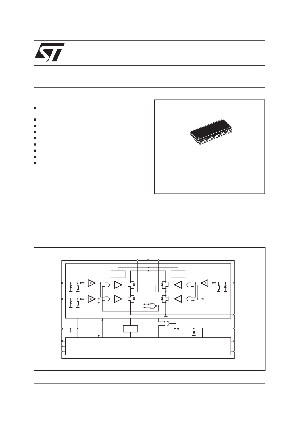
L9925
SO28
DESCRIPTION
The L9925 is a dual full bridge driver for stepper
motor applications. Realized in BCD (Bipolar,
CMOS & DOS) techology, logic circuits, precise
linear blocks and power transistors are combined
to optimize circuit performance and minimize off
chip components.Schmitttriggers are used for all
input stages and are fully compatible with 5V
CMOS logic levels. When both enable signalsare
low, the IC is commanded to a low quiescentcurrent state and will draw less than 200µA from the
battery.
BLOCK DIAGRAM
OUT1 VS1 OUT2
CHARGE
PUMP
IN1
EN1
7V T1
1st FULLBRIDGE
EN1
T1T2T2
ORDERING NUMBER: L9925
The charge pump is integrated on chip; no external componentsare required. Full performanceis
maintaned for 9V <V
6V <<V
S <9V and 16V <VS <40V yields full func-
S <16V. Extended ranges of
tionally but with relaxed performance. Over temperature protectionand ESD protectionto all pins
ensures relability and reduces system integration
failures.
CHARGE
PUMP
IN2
TEMP
EN1
EN1
7V7V
PGND1
GND
EN2
IN3
IN4
2nd FULLBRIDGE
T1 T2
5V
REGULATOR
40V
EN2
D99AT423
VS2
OUT3
OUT4
March 1999
...............................................................................................................................................................................................................
1/9
Page 2
L9925
ABSOLUTEMAXIMUMRATINGS
Absolute Maximum Ratings are those values beyond whih damage to the device may occur. Functional
operation underthese conditionisn’t implied.
For voltages andcurrents applied externallyto the device:
Symbol Parameter Value Unit
V
VSDC Dc Supply Voltage -0.3 to 26 V
V
VSP Supply Voltage Pulse (T ≤400ms)
I
OUT
I
OUT MAX
DC Output Load Current
DC Output Current:for VOUT > VVS +0.3V or VOUT < -0.3V
the internal DMOS reverse and/or substrate diode become
conductive and the applied current should not exceedthe
specified limit.
V
IN1,2
V
T
stg,Tj
P
EN
tot
DC Input Voltage -0.3 to 7 V
Enable Input Voltage -0.3 to 7 V
Storage and Junction Temperature -40 to 150 °C
Total Power Dissipation (T
(T
(T
(1) Device may be overstressed if pulsed simultaneous with short circuit at one or more of the outputs willbe present.
(1)
=80°C)
pins
=70°C no copper area on PCB)
amb
amb =70°C 8cm
2
copperareaon PCB)
40 V
1.2 A
±
1.8 A
±
5
1.23
2
W
W
W
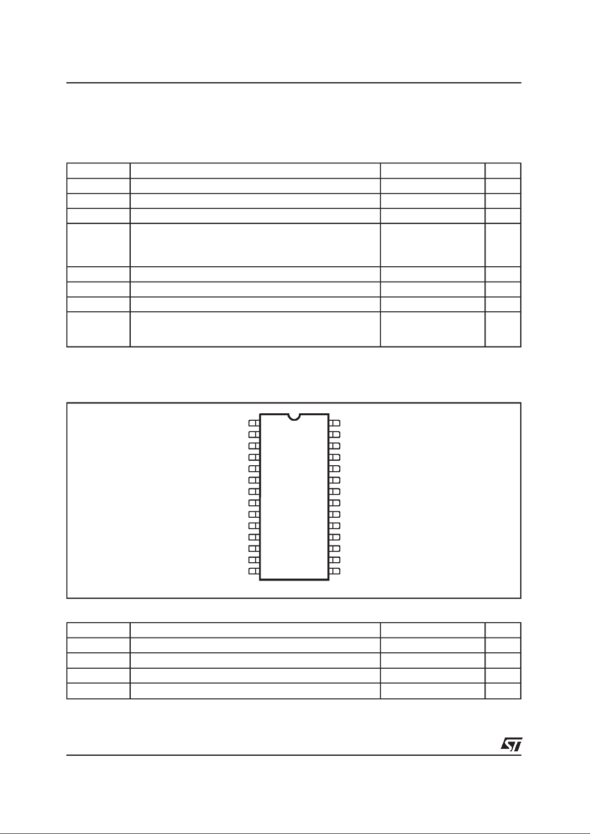
PIN CONNECTION
PGND
IN1
EN1
N.C.
N.C.
OUT1
GND
GND
OUT3 VS2
N.C. N.C.
N.C.
EN2
IN3 IN4
2
3
4
5
6
7
8
9
10
12
13
D88AT424
28
27
26
25
24
23
22
21
20
19
18
17
16
1514PGND N.C.
N.C.1
IN2
OUT2
N.C.
N.C.
VS1
GND
GND
N.C.11
OUT4
THERMAL DATA
Symbol Parameter Value Unit
T
jTS
T
jTSH
R
th j-amb
R
th j-pins
(2)
With 6cm2on board heat sink area
Thermal Shut-downjunction temperature min. 150 °C
Thermal Shut-downthereshold hysteresis typ. 25 °C
Thermal Resistance Junction-ambient
(2)
50 °C/W
Thermal Resistance Junction-pins 15 °C/W
2/9
Page 3

PIN FUNCTIONS
N. Name Function
1 PGND1 Ground for DMOS sources in bridge 1
2 IN1 Digital Input from motor controller for bridge 1
3 EN1 Logic enable/disable for bridge 1 (active high)
4, 5 NC No connect
6 OUT1 Output of one half of bridge1
7, 8 GND Ground
9 OUT3 Output of one half of bridge2
10, 11 NC No connect
12 EN2 Logic enable/disable for bridge 2 (active high)
13 IN3 Digital Input from motor controller for bridge 2
14 PGND2 Ground for DMOS sources in bridge 2
15 NC No connect
16 IN4 Digital Input from motor controller for bridge 2
17 OUT4 Output of one half of bridge 2
18, 19 NC No connect
20 VS2 Supply Voltage for bridge 2
21, 22 GND Ground
23 VS1 Supply Voltage for bridge 1
24, 25 NC No connect
26 OUT2 Output of one half of bridge 1
27 IN2 Digital Input from motor controller for bridge 1
28 NC No connect
L9925
ELECTRICALCHARACTERISTICS (VS = 9 to 16V; Tj =-40 to 150°C
(3)
, unlessotherwise specified.)
Symbol Parameter Test Condition Min. Typ. Max. Unit
T
T
T
I
R
d-on
d-SB
d-off
t
rise
t
fall
IL
S
ds
Quiescent Current EN1 = EN2 =0V; Tj=85°C 200
EN1 = EN2 =5V; I
= 0A 5 12 mA
load
Switch on Resistance Tj=25°C; VS= 14V; Io=300mA 0.75 0.8
= 125°C; VS= 6V; Io=300mA 1.5 1.9
T
j
Turn-on delay See Fig 1 10 50
Standby setting time See Fig 1 50 200
Turn-off delay See Fig 1 10 50
Output rise time (10 to 90%) See Fig 1 0.5 5 20
Output fall time (90to 10%) See Fig 1 0.5 5 20
o Output leakage current EN = 0V;Vo =VS or GND -10 10 mA
INx, ENx Logic Input Lowvoltage -0.3 1.5 V
Logic Input High voltage 3.5 6 V
Hysteresis 0.5 1.0 2.0 V
Ibias Input bias current -50 300 µA
The voltage referedto GND and currents are assumed positive, when the current flows into thepin.
(3) Tested up to 125°C, parameter guaranted by correlation up to150°C
A
µ
Ω
Ω
s
µ
s
µ
s
µ
s
µ
s
µ
3/9
Page 4

L9925
Logic Levels
All inputs are positive,non invertinglogic
Logic State Voltage Range
0 -0.3 to 1.5V
1 3.5 to 6.0V
Truth Table
Enable/Disable
EN1 EN0 Bridge 1 Bridge 2 Iq
0 0 Disabled Disabled <200µA
0 1 Disabled Enabled <12mA
1 0 Enabled Disabled <12mA
1 1 Enabled Enabled <12mA
Figure 1. TimingDiagram
STANDBY MODE OPERATING MODE OVERTEMPERATURE STANDBY MODE
EN2
EN1
IN1
GeneralOperation
With the bridge enabled, each input INx, maps directly to thecorrespondingoutput OUTx.
The output voltage will be equal to the difference
between the supply rail and the product of the
load current ad the on resistance of the output
switch.V
out =Vsupply -(RDS,ON ⋅ ILOAD).
Sourcedload currentsare positive.
IN1 OUT1 IN2 OUT2 IN3 OUT3 IN4 OUT4
00000000
1V
1VS1VS1VS
S
IN2
OUT1
OUT2
Tristate
Tristate
t
t
dSB
dON
50%
10%
t
dSB
t
r
t
r
t
dOFF
90%
t
f
t
dOFF
Figure 2. Typical RON - Characteristicsof Source
and Sink Stage
RON
(Ω)
2
1
-20 0 20 40 60 80 100 120 140 160 T(°C)
-40
V
V
D99AT426
VS
VS
=6V
=12V
t
dSB
t
f
Tristate
t
dON
Tristate
D99AT425
Tristate
Tristate
t
dSB
Figure3. ON - Resistance vs SupplyVoltage
RON
(Ω)
1.9
1.5
0.9
0.75
6
I
OUT1/2
=±0.3A
12 16.5 V
max for TJ≤125°C
typ. for T
=25°C
J
(V)
VS
D99AT427
4/9
Page 5

Figure 4. ApplicationDiagram
L9925
CEN
100nF
D
0
+5V
D
0
I/O
µP
10KΩ
I/O
I/O
EN1
O
GND
O
EN2O
OOIN3
D
R
IN1
IN4
0
1 D
1st FULL BRIDGE
2nd FULL BRIDGE
CB
100nF
CB40V
100µF
EN1
T1T2T2
T1 T2
2
40V
7V T1
CHARGE
PUMP
REGULATOR
CEN
100nF
OUT1 VS1 OUT2
TEMP
5V
R
0
10KΩ
EN1
EN2
A
CHARGE
PUMP
STEPPER MOTOR
B
IN2
7V7V
EN1
PGND1
VS2
40V
OUT3
CEX
100nF
OUT4
CEX
PGND2
100nF
D99AT423
Figure 4 shows a typical application diagram for
DC motordriving. To assure the safety of the circuit in the reverse battery conditiona reverse protetion diode D
tection diode D
supply voltage V
V
BAT line will be limited to a value lower than the
absolute maximu ratings for V
B are used to lower VS-EMR and its values de-
C
1 is necessary. The transient pro-
2 must assure that themaximum
S during the transients at the
VSP. The capacities
pend on the driving load.
The resistance feedback loop realized by R
o lim-
ited to theµP power supply line by the diode D
allows open load detection. To protect the device
at the outputsagainst EMI or ESD> 2KV external
capacitorsC
ex maybe used.
CIRCUIT DESCRIPTION
L9925 is a dual full bridge IC designed to drive
DC motors, stepper motors and other inductive
loads. Eah bridge has 4 power DMOS transistor
with R
DSon = 0.75Ω and the relative protection
and control circuitry (see fig. 5). Tthe 4 half
bridges can be controlled independently by
means of the 4 inputs IN1, IN3, IN4 and 2 enable
inputs ENABLE1and ENABLE2.
LOGIC DRIVE(true table for the two full bridges)
INPUTS
IN1
IN2
IN3
IN4
EN1 =EN2 = H L
L
H
L
L
H
H
H
@Tj > 150°C X X All transistors turned OFF
o
EN1 =EN2 = L X X All transistorsturned OFF
OUTPUT
MOSFETS
Sink 1, Sink2
Sink1, Source2
Source1, Sink2
Source1, Source2
L = Low; H = High; X = Don’t care
CROSSCONDUCTION
The device guaranteesthe absenceof cross-conduction by watching internal gate-source voltage
of the driving power DMOS.
TRANSISTOR OPERATION
ON STATE
When one of POWER DMOS transistors is ON it
can be consideredas a resistor R
DS(ON) = 0.75
at a junctiontemperatureof 25°C
Ω
5/9
Page 6

L9925
In this conditionthe dissipated power is ginen by:
P
ON =RDS(ON) ⋅ IDS
2
The low RDS(ON) of the Multipower BCD process
can provide high currents with low power dissipation.
OFF STATE
When one of the POWER DMOS transistor is
OFF the V
age and only the leakage currentI
DS voltage is equal to the supply volt-
DSSflows.
The power dissipation during this period is given
by:
P
OFF =VS ⋅IDSS
Figure 5a. Two phasechopping
EN
IN1
IN1 =
IN2 =
EN1 = H
H
L
D99AT429
IN2
TRANSITIONS
Like all MOS power transistors the DMOS
POWER transistors have an intrinsic diode between their source and drain that can operate as
a fast freewheeling diode in switched mode applications. During recirculation with the ENABLE input is low, the POWER MOS is OFF and the diode voltage it is clamped to its characteristics.
When the ENABLE input is low, the POWER
MOS is OFF and the diode carries all of the recirculationcurrent. The power dissipatedin the transitional times in the cycle depends upon the voltage and current waveformsin theapplication.
trans =IDS(t)⋅ VDS(t)
P
EN
IN1
IN1 =
IN2 =
EN1 = H
L
H
D99AT430
IN2
Figure 5b. Onephase chopping
EN
IN1
IN1 =
H
IN2 =
L
EN1 = H
Figure 5c. Enable chopping
EN
IN1
IN1 =
H
IN2 =
L
EN1 = H
D99AT431
D99AT433
EN
IN2
IN1
IN1 =
H
IN2 =
H
EN1 = H
EN
IN2
IN1
IN1 =
X
IN2 =
X
EN1 = L
D99AT432
D99AT434
IN2
IN2
6/9
Page 7

L9925
THERMAL PROTECTION
A thermalprotectioncircuit has been included that
will disable the device if the junction temperature
reaches 150°C. When the temperature has fallen
to a safe level the device restarts under the control of the input and enable signals.
APPLICATIONINFORMATION
RECIRCULATION
During recirculationwith the ENALBE input high,
the voltage drop across the transistor is R
DS(ON).
for voltages less than 0.6V and is clamped at a
voltages depending on the characteristics of the
source-drain diode for greater voltages. Although
the deviceis protectedagainstcross conduction.
POWERDISSIPATION each bridge
In order to achieve the high performanceprovided
by the L9925 some attention must be paid t ensure that it has an adequate PCB area to dissipate the heat. The forst stage of any thermal design is to calculate the dissipated power in the
application, for this example the half step operation shown in Fig. 6 is considered.
RISE TIMET
R
When an arm of the half bridge is turned on current begins to flow in the inductive load until the
maximum current I
The dissipatedenergy E
OFF/ON =[RDS(ON)
E
L is reached after a time TR,
OFF/ON.
2
I
L
⋅
2
T
R]
⋅
⋅
3
Figure 6.
commutationE
transistorsare ON E
COM. As two of the POWER DMOS
ON isgiven by:
2
ON =IL
E
⋅RDS(ON) ⋅ 2 ⋅ TON
In the commutationthe energy dissipatedis:
CON =VS ⋅IL ⋅TCOM ⋅ fSWITCH ⋅ TON
E
Where:
T
COM =CommunicationTimeandit isassumedthat:;
T
COM =trise =tfall
T
SWITCH=Chopperfrequency
FALL TIME T
F
≤20µ
s
For this example it is assumed that the energy
dissipated in this part of the cycle takes the same
form as that shown for therise time:
OFF/ON =[RDS(ON) ⋅ IL
E
2
⋅ TF] ⋅
2
3
QUIESCENTENERGY
The last contribution of the energy dissipation is
due to the quiescrent supply current and is given
by:
E
QUIESCENT =IQUIESCENT ⋅ VS ⋅ T
TOTALENERGY PER CYCLE
TOT =(2 ⋅EOFF/ON +EON +ECOM) bridge1+
E
+(2 ⋅E
OFF/ON +EON +ECOM) bridg2 +EQUIESCENT
T
switch
I
L
ON TIME T
TRT
ON
ON
T
T
OFF
F
D99AT435
During this time the energy dissipated is due to
the ON resistance of the transistors E
ON and the
The total power dissipationPDIS issimply:
E
tot
=
P
DIS
=Rise time
T
R
T
=ON time
ON
T
= Fall time
F
T
= OFF time
OFF
T
T =Period
T=T
R+TON +TF +TOFF
7/9
Page 8

L9925
DIM.
MIN. TYP. MAX. MIN. TYP. MAX.
A 2.65 0.104
a1 0.1 0.3 0.004 0.012
b 0.35 0.49 0.014 0.019
b1 0.23 0.32 0.009 0.013
C 0.5 0.020
c1 45° (typ.)
D 17.7 18.1 0.697 0.713
E 10 10.65 0.394 0.419
e 1.27 0.050
e3 16.51 0.65
F 7.4 7.6 0.291 0.299
L 0.4 1.27 0.016 0.050
S8°(max.)
mm inch
OUTLINE AND
MECHANICAL DATA
SO28
8/9
Page 9

L9925
Information furnished is believed to be accurate and reliable. However, STMicroelectronics assumes no responsibility for the consequences
of use of such information nor for any infringement of patents or other rights of third parties which may result from its use. No license is
granted by implication or otherwise under any patent or patent rights of STMicroelectronics. Specification mentioned in this publication are
subject to change without notice. This publication supersedes and replaces all information previously supplied. STMicroelectronics products
are not authorized for use as critical components in life support devices or systems without express written approval of STMicroelectronics.
The ST logo is a registeredtrademark of STMicroelectronics
1999 STMicroelectronics – Printedin Italy – All Rights Reserved
STMicroelectronics GROUP OF COMPANIES
Australia - Brazil - Canada - China - France - Germany - Italy - Japan - Korea - Malaysia - Malta - Mexico - Morocco - The Netherlands -
Singapore- Spain - Sweden- Switzerland - Taiwan - Thailand - United Kingdom- U.S.A.
http://www.st.com
9/9
 Loading...