

Page 1
MOTOR BRIDGE FOR HEADLIGHT ADJUSTMENT
FULL BRIDGE OUTPUT CONFIGURATION
WITH LOW SATURATION VOLTAGE LESS
THAN 3.2V AT OUTPUTCURRENT 0.7A
OPERATING SUPPLY VOLTAGE RANGE 7V
TO 18V.SUPPLYOVERVOLTAGEUP TO 50V
HIGH POSITIONING PRECISION AND HIGH
NOISE IMMUNITY DUE TO TRANSFER
CHARACTERISTICS WITH NEUTRAL ZONE
AND STOP RANGE THRESHOLD
FAST STOP THROUGH SHORT-CIRCUITING
THE MOTOR
MOTOR STOP STATUS IN CASE OF OPEN
INPUT CONDITION
SUPPLY OVERVOLTAGE PROTECTION
FUNCTION FOR Vs MORE THAN 18V, UP
TO 50V
INPUT PROTECTION AGAINST TRANSIENTS ON THE BATTERY LINE AND THE
REVERSEBATTERYCONDITION
THERMALOVERLOADPROTECTION
ESDPROTECTEDACCORDINGTO MIL883C
L9907N
SO20L(12+4+4)
ORDERING NUMBER: L9907ND (SO20L)
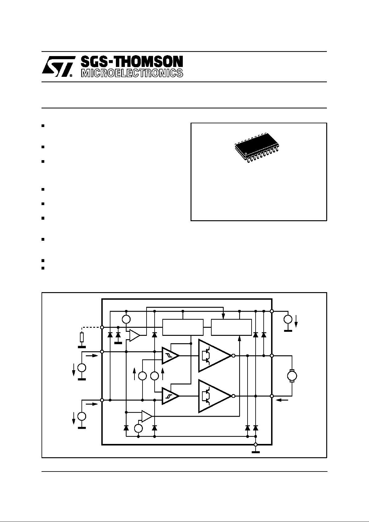
DESCRIPTION
The L9907N is a monolithic integrated power
comparator with full bridge output configuration,
intended for driving DC motors in positioning systems, optimized for headlight adjustment application and respecting the automotiveelectronics environmentalconditions.
BLOCK DIAGRAM
R
PR
V
INC
=
V
INF
=
PR
INC
I
INC
INF
I
INF
V
S
V
S
OUT C
OUT F
I
M
=
M
1.2V
=
REFERENCE
BIAS
-
+
=
=
+
-
=
1.2V
PROTECTION
FUNCTIONS
L9907N
D95AT189
GND
December 1996
1/8
Page 2
L9907N
ABSOLUTE MAXIMUM RATINGS
Symbol Parameter Value Unit
V
SDC
V
SP
I
OUT_DC
I
OUT_P
I
IN
I
IN
T
s
(*) Recommended maximal T
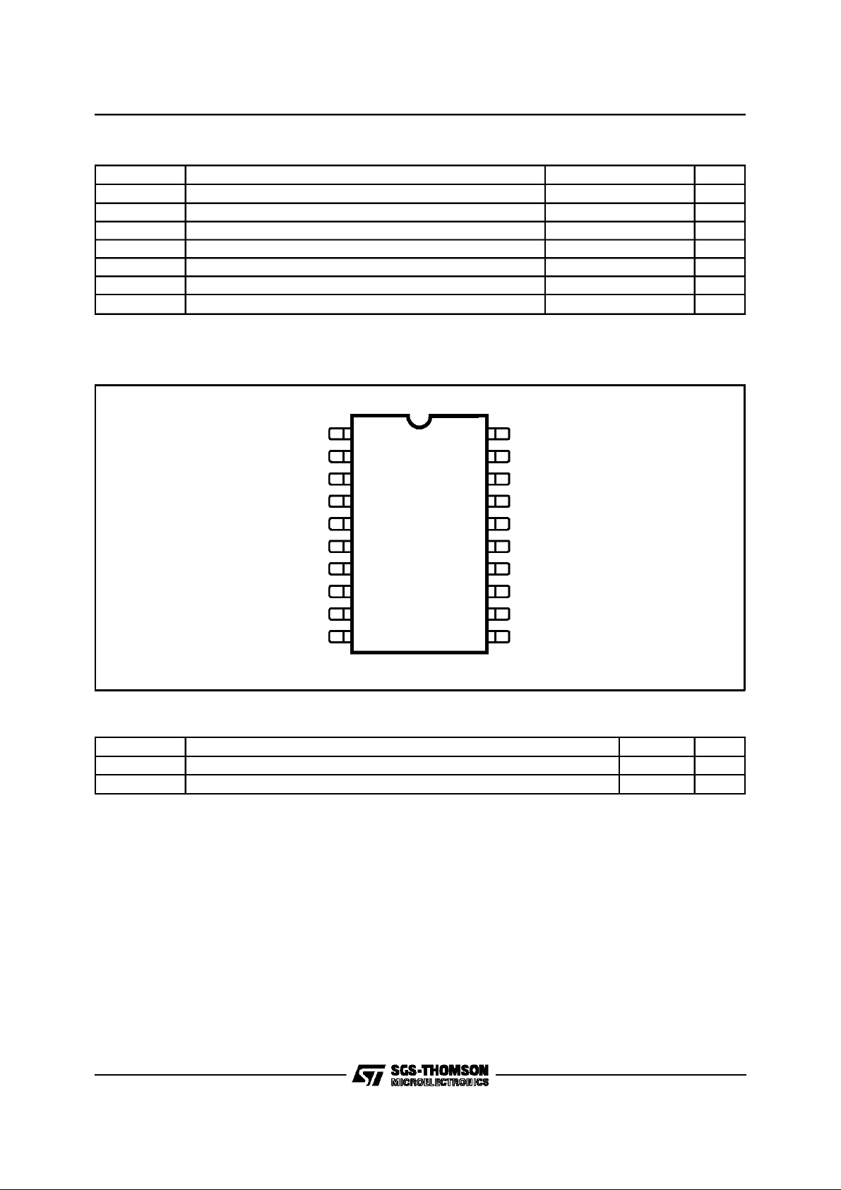
PIN CONNECTION
DC Supply Voltage 26 V
Supply Voltage Pulse (T ≤ 400ms) 50 V
DC Output Current ±0.4 A
Output Current Pulsed (100ms) 0.8 A
DC Input Current ±10 mA
Input Current Pulse (2ms) ±40 mA
Storage Shutdown Junction Temperature Range (*) 150 °C
≤ 105°C
amb
V
S
OUT
C
N.C.
GND
GND
GND
GND
N.C.
IN
C
PR N.C.
2
3
4
5
6
7
8
9
10
D95AT181
20
19
18
17
16
15
14
13
12
11
N.C.1
OUT
N.C.
GND
GND
GND
GND
N.C.
IN
F
F
THERMAL DATA
Symbol Parameter SO20L Unit
R
th j-amb
R
th j-pins
(1) with 6cm2on board heat sink area
Thermal Resistance Junction-ambient (1) 50 °C/W
Thermal Resistance Junction-pins 15 °C/W
2/8
Page 3
L9907N
ELECTRICALCHARACTERISTICS
(7V < V
< 18V, –40°C<Tj< 150°C; unless otherwise specified.)
S
Symbol Parameter Test Condition Min. Typ. Max. Unit
-V
N
-V
ST-,VST+
V
V
INCH
V
CH (3)
I
q
-, V
INCL
Quiescent Current I
Neutral Zone Threshold (2) 1.5 < V
N+
Stop Range Threshold 1.5< VINC < VS-2V;VS=12V
Control Input LOW Disable
Threshold
Control Input HIGH Disable
Threshold (4)
= 0, (Output Open)
OUT
|V
| < 20mV (stop)
din
|V
| < 200mV (L or R)
din
INC<VS
R
= ∞
PR
R
=0
PR
R
= ∞
PR
R
=0
PR
Tj= -40 to +25ºC
T
= >25ºC
j
Outputs = ON
with RINC = 0Ω
with R
with R
INC
INC
=5KΩ
= 10K
-2V; VS= 12V
Ω
3xV
3xV
25
50
0.8
0.6
ST
ST
7
6
9
7
120
2404xVST
4xV
38
76
1.2
1.2
V
V
60
100
1.5
1.5
V
S
S
S
-1.5
-1.4
mA
mA
mV
mV
ST
mV
mV
V
V
-2
V
V
V
Outputs = OFF
with R
with R
with R
I
IN
V
OSI
V
OSO
(2) With a programming resistor RPRbetweenthe PR pin and GND the N+ and N- thresholds can be adjusted from the nominalvalue (RPR= ∞
, pin PR open) up to two times the nominal value (R
The formula defining V
for R
=∞ this formula reduced to:
PR
-V
N+(RPR
in V and RPRin KΩ theseformulas result in mV
for V
s
is the controlinput voltage applied to the pin INCthrough a serial resistor R
(3) V
CH
(4) OUTPUTS = UNDEFINED for: VS-2V < VCH(R
Input Bias Current 1.5 < V
Output Saturation Voltage
Sink Stage
Output Saturation Voltage
Source Stage
PR
typicalvalue as a function of RPRand VSis: –VN−= VN+=(36mV + 0.017⋅ VS) ⋅
N+,VN-
= ∞)=VN+(RPR= ∞) = 18mV + 0.0086 ⋅ VS.
-1.5V< VCH(R
V
S
-1.4V< VCH(R
V
S
INC
INC
INC
V
din
V
din
V
din
V
din
I
OUT
I
OUT
I
OUT
I
OUT
= 0,pin PR shorted to GND).
=0Ω)<VS-0.8V
=5KΩ)<VS-0.6V
= 10KΩ)<VS-0.4V
=0Ω
INC
=5K
= 10KΩ
INC<VS
Ω
-2V; VS= 12V
∞
INC
INC
=0;RPR=
= ± 200mV; RPR= ∞
=0;RPR=0
=±200mV; RPR=0
= 0.7A
= 0.35A
= 0.7A
= 0.35A
INC
V
-0.8
S
V
-0.6
S
V
-0.4
S
R
PR
R
PR
9.5KΩ
2.0
4.0
3.6
6.8
1.4
1.1
2
1.5
.
1 +
1 + 2 ⋅
0.45
0.9
0.8
1.5
1.1
0.8
1.2
0.9
9.5KΩ
V
V
V
µ
µA
µA
µ
V
V
V
V
A
A
Figure 1: L9907NDifferential Input to OutputTransfer Characteristics
VM=V
OUTC-VOUTF
V
N-
MOTOR
DIRECTION RIGHT
D95AT182
V
H-
V
N+
V
H+
STOP RANGE
MOTOR
DIRECTION LEFT
V
INC-VINF
NEUTRALZONE
3/8
Page 4

L9907N
FUNCTIONAL DESCRIPTION
The L9907N is a power comparator with fullbridge push-pull outputs, intended for driving a
DC motor in the headlingadjustmentsystem.
The basic function of the device is shown in the
input-outputtranfer characteristic, Fig. 1.
For differential input voltage (V
INC-VINF
than the negativeNEUTRALZONE threshold, V
) lower
N-
the output voltage is negative (corresponds to
motor direction right), for increasingdifferential input voltage,this status changesto the zero output
voltage (motor is actively braked), when the differential input voltage exceeds the V
stop range
ST-
threshold. The outputstatusremains in thiscondition as long as the differential input voltage remains within the NEUTRAL ZONE. If the input
voltage increases above the positive NEUTRAL
ZONE threshold V
, the output voltage become
N+
positive(motor direction left).
Similar behaviour is obtained for decreasing the
input voltage. The output status transitions are
marked with the arrows showing the corresponding direction of the output status variation. The
active braking mode is got with both outputs in
”HIGH” status
The above described behaviour assures high positioning precision, corresponding to the STOP
RANGE and high noise immunity in the adjusted
condition due to the NEUTRAL ZONE hysteresis
thresholds.
Both the above described thresholds are defined
referring to I
Figure 3:
RecommendedApplicationCircuit Diagram with L9907N for trackingregulation
(V
NC,INF
F=VC
pins. The error due to voltage
for 1.5V < VC<VS-2V):
drop over the input signal source resistances
R
INC,RINF
bias currents I
The above mentioned resistors (R
is minimized with extremely low input
INC,IINF
.
,R
INF
) are
INC
necessary for the input current limitation during
the transients on the V
line. The input source
BAT
resistors must be dimensioned so that in case of
a line transient the input current in the input pin,
clamped with the internal input protection diodes
do not increase over the specified absolute maximum value.
Figure2: Controlto feedbacktransf ercharacter i s ti c
-2V
S
within
D95AT183A
V
BAT
for trackingregulation (V
the nominal V
V
BAT
VS-2V
V
F
1.5V
0
1.5V V
operatingrange):
INC
V
C
F=VC
V
BAT
R
Note:
Recommended value of R
input voltage |V
motor will not change its previous position.
INC-VINF
INC,RINF
| remains withintheNEUTRAL ZONE, when the control signal wire become broken. When this condition is fulfiled the
D1
D2 C
C
V
C
(equivalent input resistance to INCand INF)is5KΩto 10KΩ. Resistor RCFshould assure that the differential
4/8
MODULE
I
Q
V
S
R
PR
R
INC
V
R
CF
INC
R
INF
V
INF
I
I
PR
INC
INC
INF
INF
S
L9907N
GND
OUT C
M
OUT F
D95AT184
R
F
MV
V
I
M
F
Page 5

L9907N
An external resistor RCFis recommended between the slider of the control and feedback potentiometer.
This resistor assures that in the case of input control or input feedback wire interruption the input
differential voltage will be within the NEUTRAL
ZONE and the motor position remains frozen.
The circuit features an overvoltage disable function referred to the supply voltage V
higher than
S
18V, both outputs are forced to tristatein thiscondition.
The thermal overload function disables the outputs (tristate) when the junction temperature increases above the thermal shutdown threshold
temperatureof min. 150°C.
For the start of a heavyloaded motor, if the motor
current reaches the max. value it is necessary to
respect the dynamical thermal resistance junction
to ambient. The maximum output current is 0.8A.
The maximum junction temperature in this phase
should not increase above the thermal shutdown
threshold. In case of output disable due to thermal overload the output remains disabled till the
junction temperaturedecreasesunder the thermal
enable threshold. This behaviour is assured with
the thermal shutdownhysteresis threshold, which
minimum value is 20°C.
Figure 3, 5 and 7 show typical application diagrams for headlight adjustment applications. To
assurethe safety ofthe circuitsin the reversebattery condition a reverse protection diode D
,is
1
necessary.
The input currents in this condition are limited by
the resistors R
tion diode D
ing forV
2
during the transients at V
S
and R
INC
must assure that the maximum rat-
. The transient protec-
INF
line will be
BAT
limited to a value lower than absolute maximum
Figure4:
Controlto feedbacktransfercharacteris tic
for proportionalregulatio n withextended
operating range:
V
C
V
BAT
D95AT185A
V
BAT
VS-2V
V
F
1.5V
0
1.5V V
V
C
-2V
S
Figure 5:
Note:
Recommended value of R
the control signal wire become open, R
Recomm end edApplicationCircuitDiagramwith L9907Nfor proportionalregulationwith extended
operatingrange. For ideal adjusted condition VF=
V
C
V
BAT
R
INC,RINF
D1
D2 C
C
V
(equivalentinput resistanceto INCand INF)is5KΩto10KΩ. If themotor shouldnot change itsposition, when
R
INC2
R
+ R
INC1
I
Q
V
S
R
PR
R
INC1
V
R
INC2
C
INC1
and R
should be rated so that V
INC2
INC
R
INF
V
INF
I
I
PR
INC
INC
INF
INF
S
L9907N
GND
≤
0.4V in this condition.
INC
INC2
OUT C
M
OUT F
D95AT186
⋅ VC:
I
M
MODULE
R
F
MV
V
F
5/8
Page 6

L9907N
Figure 6: Controlto feedbacktransfercharacteris tic
forproportionalregulation with reduced
operatingrange:
V
C
-2V
S
D95AT187A
V
V
C
BAT
V
BAT
VS-2V
V
F
1.5V
Figure 7:
0
1.5V V
ALLOWED VC OPERATINGRANGE
RecommendedApplicationCircuitDiagramwith L9907Nfor proportionalregulationwith reduced
operatingrange. For ideal adjusted condition VF=
V
C
rating for VS. The device features an output disable function in case of controlinput voltage overdrive.
When the control input voltage increases above
the HIGH control input disable threshold V
V
, typically VS-1.2V or decreases below the
INCH
LOW control input disable threshold V
INC
INC>VINCH
typically 1.2V, then both outputs will be forced to
tristate.
NC
The potential of the I
pin is clamped at the Control Input HIGH disable threshold potential with a
series resistor of 5KΩ typ. To activate the HIGH
disable comparator an input current of 35µA typ.
is needed. To respect this behaviour in the applicationV
isspecified for differentR
CR
R
R
INF2
INF2
+
R
⋅ VC:
INF2
INC.
MODULE
>
,
V
BAT
R
Note:
Recommended value of R
input voltage |V
motor will not change its previous position.
INC-VINF
INC,RINF
| remainswithin the NEUTRAL ZONE,when the control signal wire become broken. When this condition is fulfilled the
D1
D2 C
C
V
C
(equivalent input resistance to INCand INF)is5KΩto 10KΩ. Resistor RCFshould assure that the differential
I
Q
V
S
R
PR
R
INC
V
R
CF
INC
R
INF1
V
INF
I
I
INC
INF
INC
INF
R
PR
INF2
S
L9907N
GND
OUT C
M
OUT F
D95AT188
R
F
MV
V
I
M
F
6/8
Page 7

SO20 PACKAGEMECHANICAL DATA
L9907N
DIM.
MIN. TYP. MAX. MIN. TYP. MAX.
A 2.65 0.104
a1 0.1 0.3 0.004 0.012
a2 2.45 0.096
b 0.35 0.49 0.014 0.019
b1 0.23 0.32 0.009 0.013
C 0.5 0.020
c1 45° (typ.)
D 12.6 13.0 0.496 0.512
E 10 10.65 0.394 0.419
e 1.27 0.050
e3 11.43 0.450
F 7.4 7.6 0.291 0.299
L 0.5 1.27 0.020 0.050
M 0.75 0.030
S8°(max.)
mm inch
7/8
Page 8

L9907N
Information furnished is believed to be accurate and reliable. However, SGS-THOMSON Microelectronics assumes no responsibility for the
consequences of use of such information nor for any infringement of patents or other rights of third parties which may result from its use. No
license is granted by implicationor otherwise under any patent or patent rights of SGS-THOMSON Microelectronics. Specification mentioned
in this publication are subject to change without notice. This publication supersedes and replaces all information previously supplied.
SGS-THOMSON Microelectronics products are notauthorized foruseas criticalcomponents in life support devices or systems without express
written approval of SGS-THOMSON Microelectronics.
1996 SGS-THOMSON Microelectronics – Printedin Italy – AllRights Reserved
SGS-THOMSON Microelectronics GROUP OF COMPANIES
Australia - Brazil - Canada - China - France - Germany - HongKong - Italy - Japan - Korea - Malaysia - Malta - Morocco - The Netherlands -
Singapore - Spain - Sweden - Switzerland- Taiwan- Thailand - United Kingdom - U.S.A.
8/8
 Loading...