

Page 1
L9822N
OCTALSERIAL SOLENOID DRIVER
.EIGHTLOWR
(0.5ΩATI
=1A@25°CVCC=5V±5%)
O
DMOSOUTPUTS
DSon
.8 BITSERIAL INPUT DATA (SPI)
.
8 BIT SERIAL DIAGNOSTIC OUTPUT FOR
OVERLOADANDOPENCIRCUITCONDITIONS
.
OUTPUT SHORT CIRCUITPROTECTION
.CHIPENABLESELECTFUNCTION(activelow)
.INTERNAL 35V CLAMPINGFOR EACH OUT-
PUT
.CASCADABLE WITH ANOTHER OCTAL
DRIVER
.LOWQUIESCENTCURRENT (10mAMAX.)
.
PACKAGE PowerSO20
DESCRIPTION
TheL9822N is an octal low side solenoiddriver
realizedin Multipower-BCDtechnologyparticularly
suitedfor drivinglamps,relaysandsolenoidsin au-
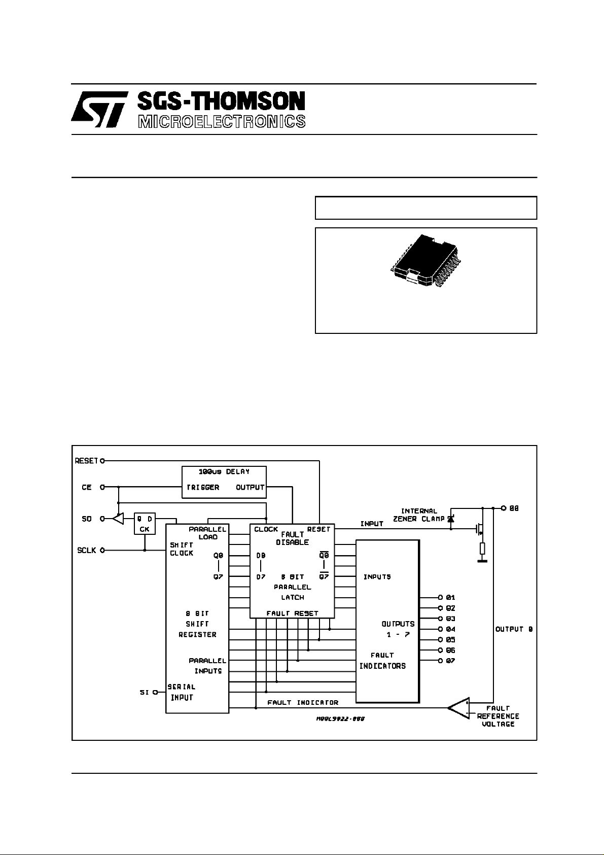
BLOCKDIAGRAM
MULTIPO WER BCD TECHNOLOG Y
PowerSO20
ORDERINGNUMBER: L9822N
tomotive environment. The DMOS outpts L9822N
has a verylow power consumption.
Data is transmitted serially to the device usingthe
SerialPeripheralInterface(SPI)protocol.
The L9822Nfeaturestheoutputsstatusmonitoring
function.
October1997
1/9
Page 2
L9822N
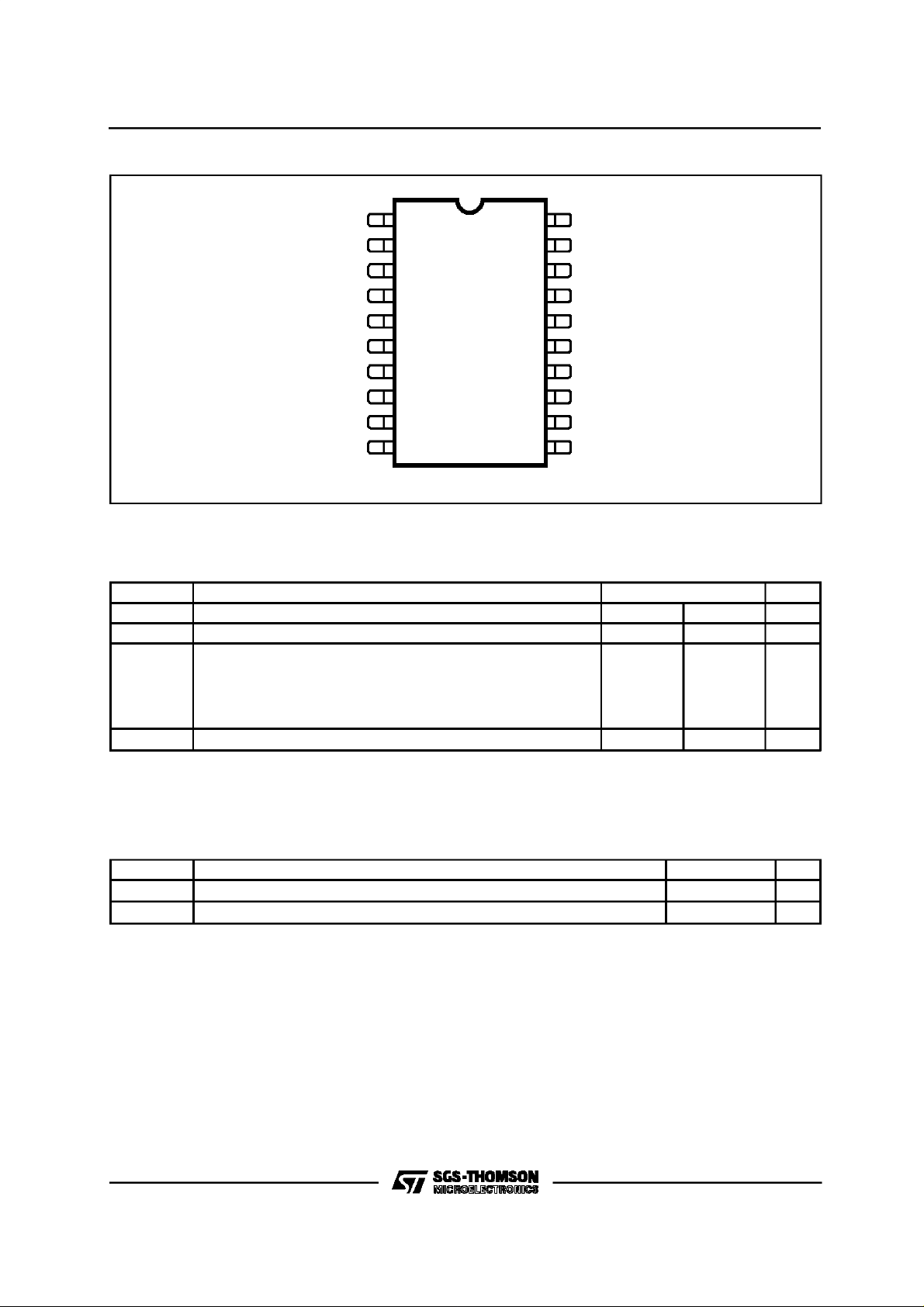
PIN CONNECTIONS
(topview)
RESET
GND
2
3
V
SO
CC
4
OUT7
OUT6
OUT5
OUT4
N.C. N.C.
GND GND
5
6
7
8
9
10
D94AT119A
20
19
18
17
16
15
14
13
12
11
GND1
SI
SCLK
CE
OUT0
OUT1
OUT2
OUT3
ABSOLUTEMAXIMUM RATINGS
Symbol Parameter Value Unit
DC Logic Supply – 0.7 7 V
Output Voltage – 0.7 40 V
Input Transient Current
(CE, SI, SCLK, RESET, SO) :
Duration Time t = 1s,
<0
V
I
V
I>VCC
Junction and Storage Temperature Range – 40 150
stg
–25
+25
T
j
V
CC
V
O
I
I
,T
mA
mA
°
C
THERMAL DATA
Symbol Parameter Value Unit
Thermal Resistance Junction-Case Max. 1.5
Thermal Resistance Junction-Ambient Max. 60
2/9
R
th j-case
R
th j-amb
C/W
°
C/W
°
Page 3
PIN DESCRIPTION
L9822N
V
CC
Logicsupplyvoltage - nominally 5V
GROUND
DeviceGround.Thisgroundappliesforthelogiccircuitsas well as the poweroutputstages.
RESET
Asynchronousresetfortheoutputstages,theparal-
lellatchand the shiftregisterinsidetheL9822NSP.
Thispin isactivelowandit mustnotbe left floating.
Apoweronclearfunctionmaybe implementedconnectingthis pin to V
withan externalresistorand
CC
to groundwith an externalcapacitor.
CE
ChipEnable. Datais transferredfromthe shift registerstotheoutputson the risingedgeof thissignal.
Thefalling edgeof this signalsets the shiftregister
with the outputvoltagesensebits coming from the
output stages.The output driver for the SO pin is
enabledwhen this pinis low.
SO
SerialOutput.This pin is theserialoutputfrom the
shift register andit is tri-stated when CE is high.A
highfor a data biton thispin indicatesthat the par-
ticularoutput is high. A low on thispin for adatabit
indicatesthat the outputis low.
Comparing the serial output bits with the previous
serial input bits the external microcontroller implementsthediagnosticdata supplied by theL9822.
SI
SerialInput.Thispin is theserialdata input.A high
onthispinwillprogramaparticularoutputtobeOFF,
whilea lowwill turn itON.
SCLK
SerialClock.This pin clocksthe shift register.New
SO data will appearon every rising edgeof thispin
andnewSIdatawillbe latchedoneverySCLK’sfallingedgeinto theshiftregister.
OUTPUTS00-07
Poweroutputpins.The inputandoutputbitscorres-
pondingto07 aresentandreceivedfirstviatheSPI
bus and 00is thelast.
The outputs are provided with current limiting and
voltagesensefunctionsfor fault indicationand protection.The nominal load current for theseoutputs
is 500mA. Theoutputsalsohave on boardclamps
set at about 36V for recirculation of inductiveload
current.
ELECTRICALCHARACTERISTICS (V
Symbol Parameter Test Conditions Min. Typ. Max. Unit
Output Clamping Volt. IO= 0.5A, Output Programmed OFF 30 35 40 V
Out. Clamping Energy IO= 0.5A, When ON 20 mJ
Out. Leakage Current VO= 24V, Output Progr. OFF 1 mA
On Resistance Output Progr. ON
Turn-on Delay IO= 500mA
Turn-off Delay IO= 500mA
Fault Refer. Voltage Output Progr. OFF
Fault Reset Delay
(after CE L to H
transition)
Output OFF Voltage Output Pin Floating.cOutput Progr. OFF, 1.0 V
R
V
V
V
OC
E
OC
I
OFF
DSon
t
PHL
t
P
OREF
t
UD
OFF
=5V±5%.Tj=– 40to 125°C ; unlessotherwise speciifed)
CC
= 0.5A
I
O
= 0.75A
I
O
=1A
I
O
With Fault Reset Disabled
No Reactive Load
No Reactive Load
1.6 2 V
Fault detected if V
See fig. 3 75 250
O>VOREF
0.53
0.53
0.53
1
1
1
10
10
Ω
Ω
Ω
s
µ
s
µ
s
µ
3/9
Page 4

L9822N
ELECTRICALCHARACTERISTICS (Continued)
Symbol Parameter Test Conditions Min. Typ. Max. Unit
INPUTBUFFER(SI, CE, SCLKand RESETpins)
V
T–
Threshold Voltage at
Falling Edge
V
T+
Threshold Voltage at
Rising Edge
V
C
H
I
I
Hysteresis Voltage VT+–V
T–
Input Current VCC= 5.25V, 0 < VI<V
Input Capacitance 0 < VI<V
I
CC
CC
OUTPUT BUFFER(SOpin)
V
SOL
V
SOH
I
SOtl
C
SO
I
CC
Output LOW Voltage IO= 1.6mA 0.4 V
Output HIGH Voltage IO= 0.8mA V
Output Tristate Leakage
Current
Output Capacitance 0 < VO<V
0<VO<VCC, CE Pin Held High,
V
= 5.25V
CC
CC
CE Pin Held High
Quiescent Supply
Current at V
CC
Pin
All Outputs Progr. ON. I
O
per Output Simultaneously
= 0.5A
SERIALPERIPHERAL INTERFACE (see fig.2, timingdiagram)
f
op
t
lead
t
lag
t
wSCKH
t
wSCKL
t
su
t
H
t
EN
t
DIS
t
t
rSO
t
fSO
t
rSI
t
fSI
t
ho
V
Operating Frequency D.C. 2 MHz
Enable Lead Time 250 ns
Enable Lag Time 250 ns
Clock HIGH Time 200 ns
Clock LOW Time 200 ns
Data Setup Time 75 ns
Data Hold Time 75 ns
Enable Time 250 ns
Disable Time 250 ns
Data Valid Time 100 ns
Rise Time (SO output) VCC= 20 to 70% CL= 200pF 50 ns
Fall Time (SO output) VCC= 70 to 20% CL= 200pF 50 ns
Rise Time SPI
VCC= 20 to 70% CL= 200pF 200 ns
Inputs (SCK, SI, CE)
Fall Time SPI
VCC= 70 to 20% CL= 200pF 200 ns
Inputs (SCLK, SI, CE)
Output Data Hold Time 0 ns
0.2V
CC
0.7V
1.45 V
–10 +10
CC
– 1.3V
–10 10
V
V
CC
µ
20 pF
V
µA
20 pF
10 mA
A
4/9
Page 5

FUNCTIONALDESCRIPTION
TheL9822NDMOSoutputis a low operatingpower
device featu-ring, eight 1Ω R
DMOS drivers
DSON
with transient protection circuits in output stages.
Eachchannelis independentlycontrolledbyan outputlatchanda commonRESETlinewhichdisables
all eightoutputs.The driver has low saturationand
shortcircuitprotectionandcandriveinductiveandresistive loads such as solenoids, lamps and relais.
DataistransmittedtothedeviceseriallyusingtheSerialPeripheralInterface(SPI)protocol.Thecircuitreceives8 bit serialdata by meansof the serial input
(SI)which is storedin an internal register to control
theoutputdrivers.Theserialoutput(SO)provides 8
bit ofdiagnosticdata representingthe voltage level
at thedriver output.Thisallows themicroprocessor
to diagnosetheconditionof theoutputdrivers.
The output saturation voltage is monitored by a
comparatorfor an outof saturationconditionandis
abletounlatchtheparticulardriverthroughthefault
resetline. Thiscircuitis also cascadablewith another octal driver in orderto jam 8 bit multiple data.
The device is selected when the chip enable (CE)
lineis low.
Additionallythe (SO) is placed in a tri-state mode
when the deviceis deselected.The negativeedge
of the(CE) transfersthe voltagelevelof thedrivers
tothe shiftregisterand thepositiveedgeofthe(CE)
latchesthenewdatafromtheshiftregistertothedrivers. WhenCE is Low, data bit containedinto the
shift register is transferred to SO output at every
SCLKpositivetransitionwhiledatabitpresentat SI
inputis latchedintotheshiftregisteroneverySCLK
negativetransition.
InternalBlocks Description
The internalarchitectureof the deviceis based on
the threeinternalmajorblocks: the octalshiftregisterfortalkingto the SPIbus,the octallatchfor holdingcontrolbits writtenintothe deviceandthe octal
load driverarray.
L9822N
Individualregisters in the latch may be clearedby
fault conditions in order to protectthe overloaded
outputstages.The entire latchmay also becleared
by theRESET signal.
OutputStages
Theoutputstagesprovidean activelowdrivesignal
suitable for 0.75A continuous loads. The outputs
haveinternalzeners set to 36voltsto clampinductive transients at turn-off. Each output also has a
voltagecomparatorobservingtheoutputnode.Ifthe
voltageexceeds1.8V on an ON outputpin, a fault
conditionis assumedand thelatchdriving thisparticularstageis reset,turningthe outputOFFtoprotect it. The timing of this actionis describedbelow.
These comparators also provide diagnostic feedbackdatatothe shiftregister.Additionally,thecomparatorscontainan internalpulldowncurrentwhich
will cause the cell to indicatea lowoutputvoltageif
the outputis programmed OFF and the output pin
is open circuited.
TIMINGDATA TRANSFER
Figure#2 showsthe overall timing diagramfrom a
byte transfer to and fromthe L9822NSPusing the
SPIbus.
CE Highto LowTransition
Theactionbeginswhenthe ChipEnable(CE)pinis
pulledlow.Thetri-stateSerialOutput(SO)pin driver
willbeenabledentire timethatCE islow.Atthefallingedge of theCEpin,thediagnosticdata fromthe
voltagecomparatorsin theoutputstageswillbelatched into the shift register.If a particularoutput is
high, a logic one will be jammedinto that bit in the
shiftregister.Iftheoutputis low,a logiczerowillbe
loadedthere.Themostsignificantbit(07)shouldbe
presentedat theSerialInput(SI) pin. A zeroat this
pin will programan outputON,whilea one will programthe outputOFF.
Shift Register
The shiftregisterhas bothserialandparallelinputs
and serial and parallel outputs.Theserial input acceptsdatafromthe SPIbusandtheserialoutputsimultaneously sends data into the SPI bus. The
paralleloutputsarelatchedintotheparallellatchinside the L9822N at the end of a datatransfer.The
parallelinputs jam diagnosticdata intothe shift registerat thebeginningof a datatransfercycle.
ParallelLatch
The parallellatchholdstheinputdatafromtheshift
register.This data then actuatestheoutputstages.
SCLK Transitions
The Serial Clock(SCLK) pin shouldthenbe pulled
high.Atthispointthediagnosticbit fromthe mostsignificantoutput(07)willappearattheSOpin.Ahigh
here indicates that the 07 pin is higher than 1.8V.
TheSCLKpinshouldthenbe toggledlowthenhigh.
NewSOdatawillappearfollowingeveryrisingedge
of SCLK and new SI data will be latched into the
L9822Nshift register on the falling edges.An unlimitedamountofdatamaybeshiftedthroughthedeviceshiftregister(intotheSIpinandouttheSOpin),
allowingthe otherSPI devicesto be cascadedin a
daisychainwiththe L9822N.
5/9
Page 6

L9822N
CELow to HighTransition
Once the last data bit has been shifted into the
L9822NSP,theCE pin shouldbe pulled high.
Attherisingedgeof CE the shiftregisterdataislatchedintotheparallellatchandtheoutputstageswill
beactuatedbythe newdata.An internal160µsdelaytimerwillalso be startedat thisrisingedge (see
). During the 160µs period, the outputs will be
t
UD
protectedonlyby the analogcurrentlimiting circuits
since the resetting of the parallel latches by faults
conditionswillbeinhibitedduringthisperiod.Thisallowsthe part toovercomeany highinrushcurrents
that may flow immediately after turn on. Once the
delay period has elapsed, the outputvoltages are
sensedbythe comparatorsand anyoutputwithvoltageshigherthan1.8VarelatchedOFF.Itshouldbe
notedthat the SCLK pin shouldbe low at both transitionsof the CE pin to avoidany false clocking of
theshiftregister.TheSCLKinputis gatedbytheCE
Figure 1 : ByteTiming withAsynchronousReset.
pin, so that the SCLK pin is ignored whenever the
CE pinis high.
FAULTCONDITIONSCHECK
Checkingforfaultconditionsmaybe donein thefol-
lowing way. Clock in a new controlbyte. Wait 160
microseconds or so to allow the outputsto settle.
Clockinthesamecontrolbyteandobservethediagnosticdata that comes outof the device.The diagnostic bits should beidentical to the bits that were
firstclockedin. Anydifferenceswouldpointtoa fault
onthatoutput.IftheoutputwasprogrammedONby
clockingina zero,anda one camebackas the diagnosticbitforthatoutput,theoutputpinwasstillhigh
anda shortcircuit oroverloadconditionexists.Ifthe
output was programmedOFF by clocking in a one,
and a zerocameback as thediagnosticbit for that
output,nothinghad pulledtheoutputpin highandit
must befloating,so an open circuitconditionexists
for that output.
6/9
Page 7

L9822N
Figure 2
: TimingDiagram.
Figure 3 : TypicalApplication Circuit.
N
7/9
Page 8

L9822N
PowerSO20 PACKAGE MECHANICAL DATA
DIM.
mm inch
MIN. TYP. MAX. MIN. TYP. MAX.
A 3.60 0.1417
a1 0.10 0.30 0.0039 0.0118
a2 3.30 0.1299
a3 0 0.10 0 0.0039
b 0.40 0.53 0.0157 0.0209
c 0.23 0.32 0.009 0.0126
D (1) 15.80 16.00 0.6220 0.6299
E 13.90 14.50 0.5472 0.570
e 1.27 0.050
e3 11.43 0.450
E1 (1) 10.90 11.10 0.4291 0.437
E2 2.90 0.1141
G 0 0.10 0 0.0039
h 1.10
L 0.80 1.10 0.0314 0.0433
N
S
10°(max.)
8° (max.)
T 10.0 0.3937
(1) ”D and E1” do not include mold flash or protrusions
- Mold flash or protrusions shall not exceed 0.15mm (0.006”)
E2
hx45°
NN
a2
A
b
DETAILA
e3
e
R
DETAILB
D
1120
E1
T
110
PSO20MEC
lead
a3
Gage Plane
E
DETAILB
0.35
S
a1
L
c
DETAIL A
slug
-C-
SEATING PLANE
GC
(COPLANARITY)
8/9
Page 9

L9822N
Information furnished is believed to be accurate and reliable. However, SGS-THOMSON Microelectronics assumes no responsibility for
the consequences of use of such information nor for any infringement of patents or other rights of third parties which may result from its
use. No license is granted by implicationor otherwise under any patent or patent rights of SGS-THOMSON Microelectronics. Specification
mentioned in this publication are subject to change without notice. This publication supersedes and replaces all information previously
supplied. SGS-THOMSON Microelectronics products are not authorized for use as critical components in life support devices or systems
withoutexpress written approval of SGS-THOMSON Microelectronics.
Australia - Brazil - Canada - China - France - Germany - Hong Kong - Italy - Japan - Korea - Malaysia - Malta - Morocco -
The Netherlands - Singapore - Spain - Sweden - Switzerland - Taiwan - Thailand - United Kingdom - U.S.A.
1997 SGS-THOMSON Microelectronics – Printed in Italy– AllRights Reserved
PowerSO-20 is a Trademark of SGS-THOMSON Microelectronics
SGS-THOMSON Microelectronics GROUP OF COMPANIES
9/9
 Loading...