

Page 1
.25APEAKOUTPUTCURRENT
.R
= 100mΩ
ON
.DIAGNOSTICAND PROTECTION
FUNCTIONS
.µP COMPATIBLE
.
GROUNDEDCASE
.INRUSHCURRENTLIMITINGCIRCUIT
DES CRIPTION
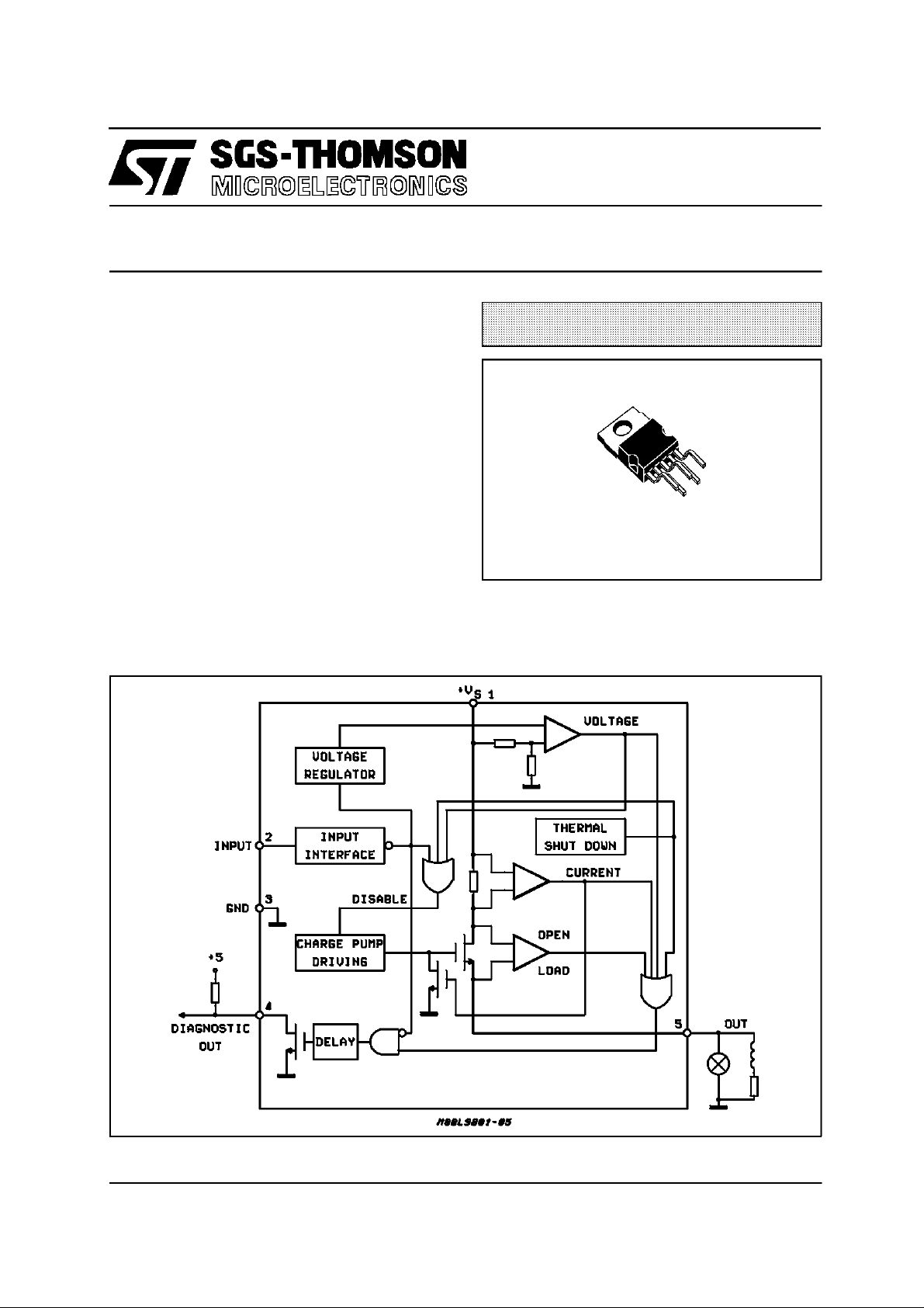
The L9821 High Side Driver realized with Multipower - BCD mixed technology,drivesresistiveor inductiveloadswith one side connectedtoground.
The inputcontrolis TTLcompatibleanda diagnostic outputprovidesan indicationof load (open and
short) and device status (thermal and overvoltage
shutdown).Onchipthermalprotectionandshortcircuitprotectionare provided.
L9821
HIGH SIDE DRIVER
MULTIPOWER BCD TECHNOLOGY
Pentawatt
ORDERING NUMBER : L9821
Thedeviceis assembledinthePentawattpackage
withthe tab connectedtothe groundterminal.
BLOCK DIAGRAM
February 1997
1/7
Page 2
L9821
ABSOLUTE MAXIMUM RATINGS
Symbol Parameter Value
Max Forward Voltage
V
S
Positive Transient Peak Voltage (dump :
5ms ≤ t
≤ 10ms, R
rise
source
≥ 0.5Ω)
– Resistive Load
– Inductive Load
Reverse Input Voltage – 0.3Vdc
Input Voltage Pin 2 (to GND)
V
I
V
Pin 4 Voltage
4
V
Pin 5 Voltage
5
(to GND)
(to GND)
Pin 1 Current
I
1
I
Pin 2 Current (forced)
2
I
Pin 4 Current (sink)
4
I
Pin 5 Current
5
Power Dissipation Internally Limited
TOT
Junction and Storage Temperature Range – 55°C to + 150°C
STG
T
P
,T
J
*due to the negativevoltage at the output during the switchingoff.
fall time constant = 100ms,
τ
f
– 0.3V / + Vs(Vs< 20V)
– 0.3V / + V
–3V/+V
50Vdc
50V (*)
Internally Limited
0.5mA
10mA
Internally Limited
60V
s(Vs
s(Vs
< 20V)
< 20V)
THERMAL DATA
Symbol Parameter Value Unit
R
th j-case
Thermal Resistance Junction-case Max 1.5 °C/W
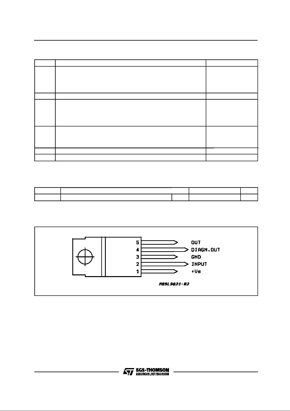
PIN CONNECTI ON (top view)
2/7
Page 3
PI N FU NCTIO NS
L9821
1. POWERSUPPLY
Supplyvoltageinput.Whenthe supply reachesthe
maximumoperatingvoltage(32V)the deviceis turned off, protectingitself and the load.
Turningoff guaranteedfor V
> 41V.
S
2. INPUT
TTL compatibleinput. High level on thispin means
outputcurrentON.Thelowlevelvoltageswitchesoff
the chargepump, thepower stage and the diagnosticoutputreducingto the minimumvaluethe quiescent current.
condition.Thisoutputdetects with Tipically45ms
delayat T
Overvoltagecondition.
-
Thermalshutdown.
-
Shortcircuit.Thepowerstagecurrentisinternally
-
limitedat 25A.
Open load. The open load conditionis detected
-
withload current< 0.6A.
=25°C thefollowing faults:
amb
The diagnosticoutput is active low. Thediagnostic
delay timeallowsto avoidspuriousdiagnosys(i.e :
turnON overcurrent,overvoltage spikesetc.).
3. GROUND
This pin must be connectedtoground.
4. DIAGNOSTICFEEDBACK
5. POWEROUTPUT
The device is provided with short circuit protection
at Vs ≤ 14.4V
The diagnosticcircuitis active in input high level
ELECTRICAL CHARACTERISTICS (V
Symbol Parameter Test Condition Min. Typ. Max. Unit
V
OP
R
ON
I
SC
I
DL
I
OPD
V
clamp
I
Off
I
ON
V
IL
V
IH
I
I
I
LEAKD
V
SATD
T
Dd
t
dON
t
r
t
dOFF
t
f
Operat. Voltage 6 32 V
On Resistance Input >2V:Tj=25°C
Short circuit current 25 A
Over Current Detection Level 20 A
Open Load Detection Level Device ON 1.2 A
Output Under Voltage Clamping I
Off State Supply Current Tj= -40 to 35°C
ON State Supply Current Tj=25°C10mA
Input Low Level 0.8 V
Input High Level 2.0 V
Input Current Vi=V
Diagnostic Output Leakage
Voltage
Diagnostic Output Saturation
Voltage
Diagnostic Delay Time Tj=25°C; 45 ms
Output ON Delay Time Tj=25°C15µs
Output ON Rise Time Tj=25°C65µs
Output OFF Delay Time Tj=25°C50
Output OFF Fall Time Tj=25°C 100
= 14.4V; -40°C ≤ Tj≤ 125°C,unless otherwise specified)
S
0.1
Input >2V:Full T range
<6A Inductive -12 -4 V
load
=35to85°C
T
j
threshold
VCC = 5V
Diagnostic Output
I
<1.6mA 0.4 V
sink
0.2
100
300
15
10 µA
Ω
µA
A
µ
A
µ
s
µ
s
µ
3/7
Page 4

L9821
FUNCTI O NAL DESCRI P TI ON
TheL9821isa highsidedrivemonolithicswitch,driven by TTL, CMOS input logic,ableto supplyresistive or inductive loads up to 6A DC allowing a
currentpeak of 25A witha R
=0.1. Theelec-
DS(ON)
tronicswitch,inadditiontoitsmainfunction,protects
itself,the power networkand the load againstload
dump(upto 60V) and overloadand it detectsshort
circuit, open load and overtemperatureconditions.
All these functions(logic controland power actuation)arepossibleonasinglechipthankstothe new
mixedSTMultipowerBCD technologythatallowsto
integrateisolatedDMOSpowertransistorsin combinationwithBipolarandCMOSsignalstructureson
the same chip.
The high side drive connection (series switch betweentheloadandthepositivepowersource)is particularlysuitedinautomotiveenvironmentwherethe
electrochemicalcorrosionwithstandinghasprimary
importance.Forthisconnectionthe best solutionis
a PowerMOS N-channelwhich requiresfordriving
only a capacitivechargepump completelyintegrated on theswitchchip.
The L9821 is based on a power DMOSserieselement,a drivingcircuitwith a chargepump,an input
logicinterfaceandonsomeprotectionandfaultdetectioncircuits.
The power DMOS transistor has a R
(typ.value@ T
of R
DS(ON)
=25°C,VGS=10V).Thelowvalue
J
is important both to increase the power
DS(ON)
= 0.1Ω
transferred to the load and to minimize the power
dissipatedin the device.
Thechargepumpisa capacitivevoltagetriplerstarting from power supply (car battery), driven by a
500kHzoscillator.
The input interfaceis based on a circuitry solution
able to guaranteethe stability over temperatureof
the TTL logic levels and very low quiescentcurrent
in OFFcondition.
When the supply reaches the maximum operating
voltage(32V) the device is turned OFF, protecting
itselfandtheload; moreoverlocalzenerclampsare
providedin somecriticalpointsto avoidthat V
GS
of
any MOS transistorcouldreachdangerousvalues
even during60V loaddumptransient.
Theinrushcurrent limiting is a significantfeatureof
theL9821.Thisfunctionallowstoprotectthepower
supplynetworkandmayextendthelifeoftheloads.
Forexample,in thecaseof thelamps,thetungsten
wireresistance value in cold conditionis aboutone
tenthofthenominalsteadystateandthentheinrush
currentduring the turn on is statisticallyone of the
main causes of lamps failures. If the high current
condition persists (e.g. load short circuit) and the
junctiontemperaturerisesabove150°C,thethermal
protectioncircuitturnsoff the devicepreventingany
damage.The current limiting and the thermalshutdownaresufficienttoprotectthedeviceagainstany
overloadbecausethepowerDMOShasnotthe second breakdown.
When the L9821 is driven and one of the protections (overtemperature, overvoltage, overload) is
present, a fault detection open drain output turns
on. This output is active also when I
load
is lower
than0.6A detectingtheopen load (disconnectedor
burned out). The diagnostic output detects fault
conditions with 25ms delay in order to avoid spurious diagnosys(i.e.: turn on overcurrent, overvoltage spikes etc.). In OFF conditions the fault
detectioncircuits arenot activeto allow a minimum
quiescentcurrent.
Thedevicecan driveunipolarDCmotorsand solenoidsaswell becauseitcanrecirculateaninductive
current when the output voltage goes lower than
value(typically- 6.5V in respect to ground).
V
clamp
The possibility to have a start up current is useful
also for DC motorsallowing the maximum starting
torque.
TYP ICAL AP PLICATION OF THE L98 2 1
The L9821 integratedhigh side driver can be used
to replacean electromechanicalrelay.
Inductiveload(i.e.solenoids,motors)canbedriven
bytheL9821.Noexternalcomponentsarerequired
forthecoilcurrentrecirculation,becausethedevice
providesthis functioninternally.
4/7
Page 5

Figure 1.
L9821
5/7
Page 6

L9821
PENTAWATT PACKAGE MECHANICAL DATA
DIM.
MIN. TYP. MAX. MIN. TYP. MAX.
mm inch
A 4.8 0.189
C 1.37 0.054
D 2.4 2.8 0.094 0.110
D1 1.2 1.35 0.047 0.053
E 0.35 0.55 0.014 0.022
F 0.8 1.05 0.031 0.041
F1 1 1.4 0.039 0.055
G 3.4 0.126 0.134 0.142
G1 6.8 0.260 0.268 0.276
H2 10.4 0.409
H3 10.05 10.4 0.396 0.409
L 17.85 0.703
L1 15.75 0.620
L2 21.4 0.843
L3 22.5 0.886
L5 2.6 3 0.102 0.118
L6 15.1 15.8 0.594 0.622
L7 6 6.6 0.236 0.260
M 4.5 0.177
M1 4 0.157
Dia 3.65 3.85 0.144 0.152
A
H3
L
L1
C
D1
Dia.
L7
L6
L2
L3L5
D
F1
H2
E
MM1
G1
G
F
6/7
Page 7

L9821
Information furnished is believed to be accurate and reliable. However, SGS-THOMSON Microelectronics assumes no responsibility for
the consequences of use of such information nor for any infringement of patents or other rights of third parties which may result from its
use. No license is granted by implication or otherwise under any patent or patent rights of SGS-THOMSON Microelectronics. Specification
mentioned in this publication are subject to change without notice. This publication supersedes and replaces all information previously
supplied. SGS-THOMSON Microelectronics products are not authorized for use as critical components in life support devices or systems
withoutexpress written approval of SGS-THOMSON Microelectronics.
Australia - Brazil - Canada - China - France - Germany - Hong Kong - Italy - Japan - Korea - Malaysia - Malta - Morocco -The Nether-
lands - Singapore- Spain - Sweden- Switzerland - Taiwan - Thailand - United Kingdom- U.S.A.
1997 SGS-THOMSONMicroelectronics – Printed in Italy – All Rights Reserved
SGS-THOMSON Microelectronics GROUP OF COMPANIES
7/7
 Loading...