

Page 1
July 2001 1/103
This is preliminary information on a new product now in development. Details are subject to change without notice.
L9805
Super Smart Power Motor Driver with 8-BIT MCU, CAN Interface, 16K EPROM, 256Bytes RAM,
128 Bytes EEPROM, 10 Bit ADC, WDG , 2 Timers , 2 PWM M odu les, Full H-Bridge Driv er
PROUCT PREVIEW
■
6.4-18V Supply Operating Range
■
16 MHz Maximum Oscillator Frequency
■
8 MHz Maximum Internal Clock Frequency
■
Oscillator Supervisor
■
Fully Static operation
■
-40°C to + 150°C Temperature Range
■
User EPROM/OTP: 16 Kbytes
■
Data RAM: 256 bytes
■
Data EEPROM: 128 bytes
■
64 pin HiQUAD64 package
■
10 multifunctional bidirectional I/O lines
■
Two 16-bit Timers, each featuring:
– 2 Input Captures
– 2 Output Compares
– External Clock input (on Timer 1)
– PWM and Pulse Generator modes
■
Two Programmable 16-bit PWM generator
modules.
■
CAN peripheral including Bus line interface
according 2A/B passive specifications
■
10-bit Analog-to-Digital Converter
■
Software Watchdog for system integrity
■
Master Reset, Power-On Reset, Low Voltage
Reset
■
70mΩ DMOS H-bridge.
■
8-bit Data Manipulation
■
63 basic Instructions and 17 main Addressing
Modes
■
8 x 8 Unsigned Multiply Instruction
■
True Bit Manipulation
■
Complete Development Support on DOS/
WINDOWS
TM
Real-Time Emulator
■
Full Software Package on DOS/WINDOWS
TM
(C-Compiler, Cross-Assembler, Debugger)
HiQUAD-64
ORDERING NUMBER: L9805
1
Page 2

2/103
Table of Contents
103
L9805
1 GENERAL DESCRIPTION . . . . . . . . . . . . . . . . . . . . . . . . . . . . . . . . . . . . . . . . . . . . . . . . . . . . . . 5
1.1 INTRODUCTION . . . . . . . . . . . . . . . . . . . . . . . . . . . . . . . . . . . . . . . . . . . . . . . . . . . . . . . . . 5
1.2 OTP, ROM AND EPROM DEVICES . . . . . . . . . . . . . . . . . . . . . . . . . . . . . . . . . . . . . . . . . . 5
1.3 PIN OUT. . . . . . . . . . . . . . . . . . . . . . . . . . . . . . . . . . . . . . . . . . . . . . . . . . . . . . . . . . . . . . . . 7
1.4 PIN DESCRIPTION . . . . . . . . . . . . . . . . . . . . . . . . . . . . . . . . . . . . . . . . . . . . . . . . . . . . . . . 8
1.5 REGISTER & MEMORY MAP . . . . . . . . . . . . . . . . . . . . . . . . . . . . . . . . . . . . . . . . . . . . . . . 9
2 CENTRAL PROCESSING UNIT . . . . . . . . . . . . . . . . . . . . . . . . . . . . . . . . . . . . . . . . . . . . . . . . . 12
2.1 INTRODUCTION . . . . . . . . . . . . . . . . . . . . . . . . . . . . . . . . . . . . . . . . . . . . . . . . . . . . . . . . 12
2.2 CPU REGISTERS . . . . . . . . . . . . . . . . . . . . . . . . . . . . . . . . . . . . . . . . . . . . . . . . . . . . . . . 12
3 CLOCKS, RESET, INTERRUPTS & POWER SAVING MODES . . . . . . . . . . . . . . . . . . . . . . . . 14
3.1 CLOCK SYSTEM . . . . . . . . . . . . . . . . . . . . . . . . . . . . . . . . . . . . . . . . . . . . . . . . . . . . . . . . 14
3.1.1 General Description . . . . . . . . . . . . . . . . . . . . . . . . . . . . . . . . . . . . . . . . . . . . . . . . . 14
3.1.2 External Clock . . . . . . . . . . . . . . . . . . . . . . . . . . . . . . . . . . . . . . . . . . . . . . . . . . . . . 15
3.2 O SCILLATOR SAFEGUARD (DCSR). . . . . . . . . . . . . . . . . . . . . . . . . . . . . . . . . . . . . . . . . 16
3.2.1 Dedicated Control Status Register . . . . . . . . . . . . . . . . . . . . . . . . . . . . . . . . . . . . . . 16
3.3 W ATCHDOG SYSTEM (WDG) . . . . . . . . . . . . . . . . . . . . . . . . . . . . . . . . . . . . . . . . . . . . . 17
3.3.1 Introduction . . . . . . . . . . . . . . . . . . . . . . . . . . . . . . . . . . . . . . . . . . . . . . . . . . . . . . . 17
3.3.2 Main Features . . . . . . . . . . . . . . . . . . . . . . . . . . . . . . . . . . . . . . . . . . . . . . . . . . . . . 17
3.3.3 Functional Description . . . . . . . . . . . . . . . . . . . . . . . . . . . . . . . . . . . . . . . . . . . . . . . 17
3.3.4 Register Description . . . . . . . . . . . . . . . . . . . . . . . . . . . . . . . . . . . . . . . . . . . . . . . . . 18
3.4 MISCELLANEOUS REGISTER (MISCR) . . . . . . . . . . . . . . . . . . . . . . . . . . . . . . . . . . . . . 19
3.5 RESET . . . . . . . . . . . . . . . . . . . . . . . . . . . . . . . . . . . . . . . . . . . . . . . . . . . . . . . . . . . . . . . . 20
3.5.1 Introduction . . . . . . . . . . . . . . . . . . . . . . . . . . . . . . . . . . . . . . . . . . . . . . . . . . . . . . . 20
3.5.2 External Reset . . . . . . . . . . . . . . . . . . . . . . . . . . . . . . . . . . . . . . . . . . . . . . . . . . . . . 20
3.5.3 Reset Operation . . . . . . . . . . . . . . . . . . . . . . . . . . . . . . . . . . . . . . . . . . . . . . . . . . . . 20
3.5.4 Power-on Reset - Low Voltage Detection . . . . . . . . . . . . . . . . . . . . . . . . . . . . . . . . 20
3.6 INTERRUPTS . . . . . . . . . . . . . . . . . . . . . . . . . . . . . . . . . . . . . . . . . . . . . . . . . . . . . . . . . . 22
3.7 POWER SAVING MODES . . . . . . . . . . . . . . . . . . . . . . . . . . . . . . . . . . . . . . . . . . . . . . . . . 24
3.7.1 Introduction . . . . . . . . . . . . . . . . . . . . . . . . . . . . . . . . . . . . . . . . . . . . . . . . . . . . . . . 24
3.7.2 Slow Mode . . . . . . . . . . . . . . . . . . . . . . . . . . . . . . . . . . . . . . . . . . . . . . . . . . . . . . . . 24
3.7.3 Wait Mode . . . . . . . . . . . . . . . . . . . . . . . . . . . . . . . . . . . . . . . . . . . . . . . . . . . . . . . . 24
3.7.4 Halt Mode . . . . . . . . . . . . . . . . . . . . . . . . . . . . . . . . . . . . . . . . . . . . . . . . . . . . . . . . . 25
4 VOLTAGE REGULATOR . . . . . . . . . . . . . . . . . . . . . . . . . . . . . . . . . . . . . . . . . . . . . . . . . . . . . . 26
4.1 INTRODUCTION . . . . . . . . . . . . . . . . . . . . . . . . . . . . . . . . . . . . . . . . . . . . . . . . . . . . . . . . 26
4.1.1 Functional Description . . . . . . . . . . . . . . . . . . . . . . . . . . . . . . . . . . . . . . . . . . . . . . . 26
4.2 DIGITAL SECTION POWER SUPPLY . . . . . . . . . . . . . . . . . . . . . . . . . . . . . . . . . . . . . . . . 26
4.2.1 VDD Short Circuit Protection . . . . . . . . . . . . . . . . . . . . . . . . . . . . . . . . . . . . . . . . . . 27
4.3 ANALOG SECTION POWER SUPPLY . . . . . . . . . . . . . . . . . . . . . . . . . . . . . . . . . . . . . . . 27
4.3.1 VCC Short Circuit Protection . . . . . . . . . . . . . . . . . . . . . . . . . . . . . . . . . . . . . . . . . . 27
5 ON-CHIP PERIPHERALS . . . . . . . . . . . . . . . . . . . . . . . . . . . . . . . . . . . . . . . . . . . . . . . . . . . . . . 28
5.1 I/O PORTS . . . . . . . . . . . . . . . . . . . . . . . . . . . . . . . . . . . . . . . . . . . . . . . . . . . . . . . . . . . . . 28
5.1.1 Introduction . . . . . . . . . . . . . . . . . . . . . . . . . . . . . . . . . . . . . . . . . . . . . . . . . . . . . . . 28
5.1.2 Functional Description . . . . . . . . . . . . . . . . . . . . . . . . . . . . . . . . . . . . . . . . . . . . . . . 28
5.1.3 Register Description . . . . . . . . . . . . . . . . . . . . . . . . . . . . . . . . . . . . . . . . . . . . . . . . . 31
5.2 16-BIT TIMER . . . . . . . . . . . . . . . . . . . . . . . . . . . . . . . . . . . . . . . . . . . . . . . . . . . . . . . . . . 32
Page 3

3/103
Table of Contents
L9805
5.2.1 Introduction . . . . . . . . . . . . . . . . . . . . . . . . . . . . . . . . . . . . . . . . . . . . . . . . . . . . . . . 32
5.2.2 Main Features . . . . . . . . . . . . . . . . . . . . . . . . . . . . . . . . . . . . . . . . . . . . . . . . . . . . . 32
5.2.3 Functional Description . . . . . . . . . . . . . . . . . . . . . . . . . . . . . . . . . . . . . . . . . . . . . . . 32
5.2.4 Register Description . . . . . . . . . . . . . . . . . . . . . . . . . . . . . . . . . . . . . . . . . . . . . . . . . 43
5.3 PWM GENERATOR . . . . . . . . . . . . . . . . . . . . . . . . . . . . . . . . . . . . . . . . . . . . . . . . . . . . . . 49
5.3.1 Introduction . . . . . . . . . . . . . . . . . . . . . . . . . . . . . . . . . . . . . . . . . . . . . . . . . . . . . . . 49
5.3.2 Functional Description . . . . . . . . . . . . . . . . . . . . . . . . . . . . . . . . . . . . . . . . . . . . . . . 49
5.3.3 Register Description . . . . . . . . . . . . . . . . . . . . . . . . . . . . . . . . . . . . . . . . . . . . . . . . . 51
5.4 PWM I/O . . . . . . . . . . . . . . . . . . . . . . . . . . . . . . . . . . . . . . . . . . . . . . . . . . . . . . . . . . . . . . . 54
5.4.1 Introduction . . . . . . . . . . . . . . . . . . . . . . . . . . . . . . . . . . . . . . . . . . . . . . . . . . . . . . . 54
5.4.2 PWMO . . . . . . . . . . . . . . . . . . . . . . . . . . . . . . . . . . . . . . . . . . . . . . . . . . . . . . . . . . . 54
5.4.3 PWMI . . . . . . . . . . . . . . . . . . . . . . . . . . . . . . . . . . . . . . . . . . . . . . . . . . . . . . . . . . . . 54
5.5 10-BIT A/D CONVERTER (AD10) . . . . . . . . . . . . . . . . . . . . . . . . . . . . . . . . . . . . . . . . . . . 56
5.5.1 Introduction . . . . . . . . . . . . . . . . . . . . . . . . . . . . . . . . . . . . . . . . . . . . . . . . . . . . . . . 56
5.5.2 Functional Description . . . . . . . . . . . . . . . . . . . . . . . . . . . . . . . . . . . . . . . . . . . . . . . 56
5.5.3 Input Selections and Sampling . . . . . . . . . . . . . . . . . . . . . . . . . . . . . . . . . . . . . . . . 57
5.5.4 Interrupt Management . . . . . . . . . . . . . . . . . . . . . . . . . . . . . . . . . . . . . . . . . . . . . . . 57
5.5.5 Temperature Sensing . . . . . . . . . . . . . . . . . . . . . . . . . . . . . . . . . . . . . . . . . . . . . . . 57
5.5.6 Precise Temperature Measurement . . . . . . . . . . . . . . . . . . . . . . . . . . . . . . . . . . . . 57
5.5.7 Register Description . . . . . . . . . . . . . . . . . . . . . . . . . . . . . . . . . . . . . . . . . . . . . . . . . 58
5.6 CONTROLLER AREA NETWORK (CAN) . . . . . . . . . . . . . . . . . . . . . . . . . . . . . . . . . . . . . 59
5.6.1 Introduction . . . . . . . . . . . . . . . . . . . . . . . . . . . . . . . . . . . . . . . . . . . . . . . . . . . . . . . 59
5.6.2 Main Features . . . . . . . . . . . . . . . . . . . . . . . . . . . . . . . . . . . . . . . . . . . . . . . . . . . . . 60
5.6.3 Functional Description . . . . . . . . . . . . . . . . . . . . . . . . . . . . . . . . . . . . . . . . . . . . . . . 60
5.6.4 Register Description . . . . . . . . . . . . . . . . . . . . . . . . . . . . . . . . . . . . . . . . . . . . . . . . . 66
5.7 CAN BUS TRANSCEIVER . . . . . . . . . . . . . . . . . . . . . . . . . . . . . . . . . . . . . . . . . . . . . . . . . 76
5.7.1 Introduction . . . . . . . . . . . . . . . . . . . . . . . . . . . . . . . . . . . . . . . . . . . . . . . . . . . . . . . 76
5.7.2 Main Features . . . . . . . . . . . . . . . . . . . . . . . . . . . . . . . . . . . . . . . . . . . . . . . . . . . . . 76
5.7.3 Functional Description . . . . . . . . . . . . . . . . . . . . . . . . . . . . . . . . . . . . . . . . . . . . . . . 76
5.7.4 CAN Transceiver Disabling function . . . . . . . . . . . . . . . . . . . . . . . . . . . . . . . . . . . . 76
5.8 POWER BRIDGE . . . . . . . . . . . . . . . . . . . . . . . . . . . . . . . . . . . . . . . . . . . . . . . . . . . . . . . . 77
5.8.1 Introduction . . . . . . . . . . . . . . . . . . . . . . . . . . . . . . . . . . . . . . . . . . . . . . . . . . . . . . . 77
5.8.2 Main Features . . . . . . . . . . . . . . . . . . . . . . . . . . . . . . . . . . . . . . . . . . . . . . . . . . . . . 77
5.8.3 Functional Description . . . . . . . . . . . . . . . . . . . . . . . . . . . . . . . . . . . . . . . . . . . . . . . 77
5.8.4 Interrupt generation . . . . . . . . . . . . . . . . . . . . . . . . . . . . . . . . . . . . . . . . . . . . . . . . . 78
5.8.5 Operating Modes . . . . . . . . . . . . . . . . . . . . . . . . . . . . . . . . . . . . . . . . . . . . . . . . . . . 78
5.8.6 Register Description . . . . . . . . . . . . . . . . . . . . . . . . . . . . . . . . . . . . . . . . . . . . . . . . . 81
5.9 EEPROM (EEP) . . . . . . . . . . . . . . . . . . . . . . . . . . . . . . . . . . . . . . . . . . . . . . . . . . . . . . . . . 8 2
5.9.1 Introduction . . . . . . . . . . . . . . . . . . . . . . . . . . . . . . . . . . . . . . . . . . . . . . . . . . . . . . . 82
5.9.2 Functional description . . . . . . . . . . . . . . . . . . . . . . . . . . . . . . . . . . . . . . . . . . . . . . . 83
5.9.3 Register Description . . . . . . . . . . . . . . . . . . . . . . . . . . . . . . . . . . . . . . . . . . . . . . . . . 84
6 INSTRUCTION SET . . . . . . . . . . . . . . . . . . . . . . . . . . . . . . . . . . . . . . . . . . . . . . . . . . . . . . . . . . 86
6.1 ST7 ADDRESSING MODES . . . . . . . . . . . . . . . . . . . . . . . . . . . . . . . . . . . . . . . . . . . . . . . 86
6.2 INSTRUCTION GROUPS . . . . . . . . . . . . . . . . . . . . . . . . . . . . . . . . . . . . . . . . . . . . . . . . . 90
7 ELECTRICAL CHARACTERISTICS . . . . . . . . . . . . . . . . . . . . . . . . . . . . . . . . . . . . . . . . . . . . . . 93
7.1 ABSOLUTE MAXIMUM RATINGS . . . . . . . . . . . . . . . . . . . . . . . . . . . . . . . . . . . . . . . . . . . 93
7.2 POWER CONSIDERATIONS . . . . . . . . . . . . . . . . . . . . . . . . . . . . . . . . . . . . . . . . . . . . . . 94
Page 4

4/103
L9805
7.3 PACKAGE MECHANICAL DATA . . . . . . . . . . . . . . . . . . . . . . . . . . . . . . . . . . . . . . . . . . . . 96
7.4 APPLICATION DIAGRAM EXAMPLE . . . . . . . . . . . . . . . . . . . . . . . . . . . . . . . . . . . . . . . . 97
7.5 DC ELECTRICAL CHARACTERISTICS . . . . . . . . . . . . . . . . . . . . . . . . . . . . . . . . . . . . . . 98
7.6 CONTROL TIMING . . . . . . . . . . . . . . . . . . . . . . . . . . . . . . . . . . . . . . . . . . . . . . . . . . . . . . 99
7.7 O PERATING BLOCK ELECTRICAL CHARACTERISTICS . . . . . . . . . . . . . . . . . . . . . . . 100
Page 5

5/103
L9805
1 GENERAL DESCRIPTION
1.1 INTRODUCTION
The L9805 is a Super Smart Power device suited
to drive resistive and inductive lo ads under software control. It includes a ST7 microcontroller and
some pheripherals. The microcontroller can execute the software contained in the program
EPROM/ROM and drive, through dedicated registers, the power bridge.
The internal voltage regulators rated to the automotive environment, PWM modules, CAN transceiver and controller, I SO 9141 transceiver, timers, temperature sensor and the AtoD converter
allow the device to realize by itself a complete application, in line with the most common mechatronic requirements.
1.2 OTP, ROM AND EPROM DEVICES
For development pu rposes the device is available
in plastic HiQuad package without window rating
in t he OTP c lass .
Mass production is supported by means of ROM
devices.
Engineering samples could be assembled using
window packages. These are generally referenced
as “EPROM devices”.
EPROM device s are erased by expos ure to high
intensity UV light admitted through the transparent
window. This exposure discharges the floating
gate to its initial state throug h induced photo current.
It is recommended to keep the L9805 device out of
direct sunlight, since the UV content of sunlight
can be sufficient to cause functional failure. Extended exposure to room level fluorescent lighting
may also cause erasure.
An opaque coating (paint, tape, label, etc...)
should be placed over the package window if the
product is to be operated under these lighting conditions. Covering the window also reduces I
DD
in
power-saving modes du e to photo-diode leakage
currents.
An Ultraviolet source of wave length 2537 Å yielding a total integrated dosage of 15 Watt-sec/cm
2
is
required to erase the EPROM. The device will be
erased in 40 to 45minutes if such a UV lamp with a
12mW/cm
2
power rating is placed 1 inch from the
device window without any interposed filters.
OTP and EPROM devices can be programmed by
a dedicated Eprom Programming Board and software that are part of the development tool-set.
Page 6
6/103
L9805
Figure 1. L9805 Block Diagram
8-BIT CORE
ALU
ADDRESS AND DATA BUS
OSCIN
OSCOUT
10-bit ADC
WATCHDOG
OSC
Internal
CLOCK
CONTROL
ROM/O TP/EPR OM
16K
PORT A
PA0 -> PA7
OSC SAFEGUARD
PORT B
PB0 -> PB1
TIMER 1
TIMER 2
PWM 2
PWM 1
PWMI
PWMO
PWMO
AD2
AD3
AD4
RAM 256B
EEPROM 128B
V
CC
V
DD
POWER
SUPPLY
VB2
PREREGULATOR
AGND
GND
NRESET
POWER
BRIDGE
VBR
VBL
PGND
OUTR
OUTL
CAN
CONTROLLER
CAN
TRANSCEIVER
CAN_H
CAN_L
RX TX
TEMP SENSOR
PWMI
VPP/TM
VB1
Page 7
7/103
L9805
1.3 PIN OUT.
1
2
3
4
5
6
7
8
9
10
11
12
13
14
15
16
48
47
46
45
44
43
42
41
40
39
38
37
36
35
34
33
64 63 62 61 60 59 58 57 56 55 54 53
52
51
50
49
17
18
19
20
21 22 23 24
29 30 31 32
25 26
27 28
NU
NU
NU
AD3
AD2
PA1/OCMP1_1
PA0/OCMP2_1
VPP/TM
VDD
OSCIN
OSCOUT
GND
NU
VBL
VBL
VBL
NU
NU
NU
NU
NU
PB1/EXTCLK_2
NU
NU
PWMO
PWMI
NRESET
CAN_H
CAN_L
GND
VDD
VB2
VB1
VBR
VBR
VBR
NU
NU
NU
NU
NU
NU
OUTL
OUTL
OUTL
PGND
PGND
OUTR
OUTR
OUTRNUNU
VCC
AGND
AD4
PA2/ICAP2_1
PA3/ICAP1_1
PGND
PGND
PA4/EXTCLK_1
PA5/OCMP2_2
PA6/OCMP1_2
PA7/ICAP2_2
PB0/ICAP1_2
Page 8

8/103
L9805
1.4 PIN DESCRI PTION
AD2-AD4:
Analog input to ADC.
PA0/OCMP2_1-PA1/OCMP1_1:
I/Os or Output
compares on Timer 1.
Alternate function software
selectable (by setting OC2E or OC1 E in CR2 register: bit 6 or 7 at 0031h). When used as an alternate function, this pin is a pus h-pull output as requested by Timer 1. Otherwise, this pin is a triggered floating input or a push-pull output.
PA2/ICAP2_1-PA3/ICAP1_1:
I/
Os or Input cap-
tures on Timer 1.
Before using this I/O as alternate
inputs, they must be configured by software in input mode (DDR=0). In this case, these pins are a
triggered floating input. Otherwise (I/O function),
these pin are triggered floating inputs or push-pull
outputs.
PA4/EXTCLK_1:
PA4 I/O or External Clock on
Timer 1
. Before using this I/O as alternate input, it
must be configured by software in input mode
(DDR=0). In this case, this pin is a triggered floating input. Otherwise (I/O function), this pin is a triggered floating input or a push-pull output.
PA5/OCMP2_2-PA6/OCMP1_2:
I/Os or Output
Compares on Timer 2
. Alternate function software
selectable (by setting OC2E or OC1 E in CR2 register: bit 6 or 7 at 0041h). When used as alt ernate
functions, these pins are push-pull outputs as requested by Timer 2. Otherwise, these pins are triggered floating inputs or push-pull outputs.
PA7/ICAP2_2-PB0/ICAP1_2:
I/Os or Input Cap-
tures on Timer 2
. Before using these I/Os as alternate inputs, they must be configured by softw are
in input mode (DDR=0). In this case, these pins
are triggered floating inputs. Otherwise (I/O function), these pins are triggered floating inputs or
push-pull outputs.
PB1/EXTCLK_2:
PB1 I/O or External Clock on
Timer 2
. Before using this I/O as alternate input, it
must be configured by software in input mode
(DDR=0). In this case, this pin is a triggered floating input. Otherwise (I/O function), this pin is a triggered floating input or a push-pull output.
VPP/TM
: Input. This pin must be held low du ring
normal operating modes.
VDD
: Output. 5V Power supply for digital circuits,
from internal voltage regulator.
OSCIN:
Input Oscillator pin.
OSCOUT
: Output Oscillator pin.
GND:
Ground for digital circuits.
VBR:
Power supply for Right half-bridge.
OUTR:
Output of Left half-bridge.
PGND:
Ground for power transistor.
OUTL:
Output of Right half-bridge.
VBL:
Power supply for Left half-bridge.
VB1
: Power supply for voltage regulators.
VB2
: Pre-regulated voltage for analog circuits.
CAN_L:
Low side CAN bus output.
CAN_H:
High side CAN bus input.
NRESET:
Bidirectional. This active low signal forces the initialization of the MCU. This event is the
top priority non maskable interrupt. It can be us ed
to reset external peripherals.
PWMI:
PWM input.
Directly connected to Input
Capture 2 on Timer 2.
PWMO:
PWM output.
Connected to the output of
PWM2 module.
AGND:
Ground for all analog circuitry (except
power bridge)
.
VCC:
Output. 5V power supply for analog circuits,
from internal voltage regulator.
Page 9

9/103
L9805
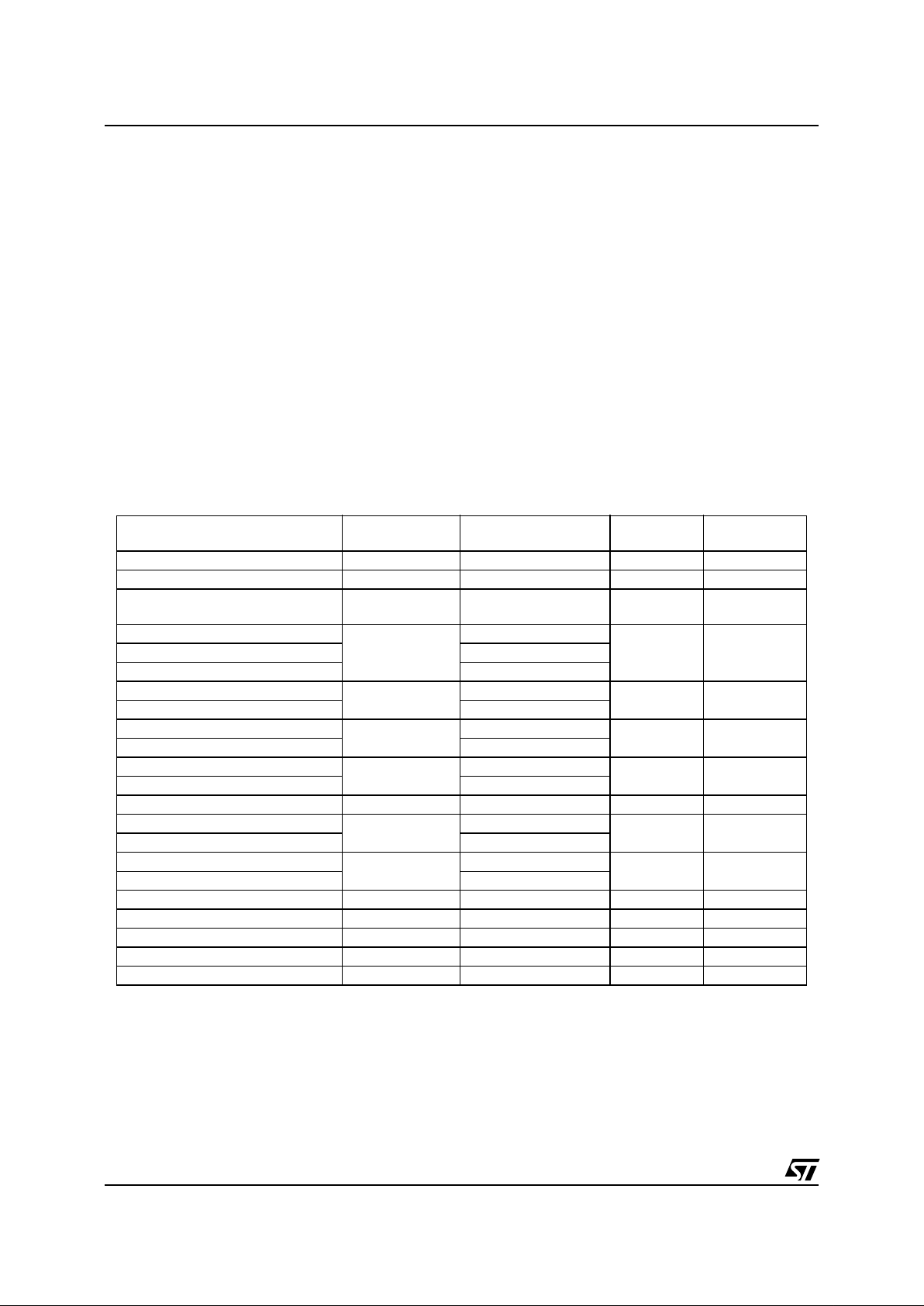
1.5 REGISTER & MEMORY MAP
As shown in the Table 1, the MCU is capable of
addressing 64K bytes of memories and I/O registers. In this MCU, 63742 of these bytes are user
acce ssib le.
The available memory locations consist of 128
bytes of I/O registers, 256 bytes of RAM, 128
bytes of EEPROM and 16Kbytes of user EPROM/
ROM. The RAM space includes 64bytes for the
stack from 0140h to 017Fh.
The highest address by tes contain the user re set
and interrupt vectors.
Table 1. Memory Map
Address Block
Register Label
Register name
Reset
Status
Remarks
0000h
0001h
0002h
0003h
Port A
PADR ..
PADDR ..
PAOR ..
Data Register
Data Direction Register
Option Register
Not Used
00h
00h
00h
R/W
R/W
R/W
Absent
0004h
0005h
0006h
0007h
Port B
PBDR ..
PBDDR ..
PBOR ..
Data Register
Data Direction Register
Option Register
Not Used
00h
00h
00h
R/W
R/W
R/W
Absent
0008h to
000Fh
RESERVED
0010h
0011h
0012h
0013h
0014h
0015h
0016h
PWM1
P1CYRH ..
P1CYRL ..
P1DRH ..
P1DRL ..
P1CR ..
P1CTH ..
P1CTL ..
PWM1 Cycle Register High
PWM1 Cycle Register Low
PWM1 Duty Register High
PWM1 Duty Register Low
PWM1 Control Register
PWM1 Counter Register High
PWM1 Counter Register Low
00h
00h
00h
00h
00h
00h
00h
R/W
R/W
R/W
R/W
R/W
Read Only
Read Only
0017h RESERVED
0018h
0019h
001Ah
001Bh
001Ch
001Dh
001Eh
PWM2
P2CYRH ..
P2CYRL ..
P2DRH ..
P2DRL ..
P2CR ..
P2CTH ..
P2CTL ..
PWM2 Cycle Register High
PWM2 Cycle Register Low
PWM2 Duty Register High
PWM2 Duty Register Low
PWM2 Control Register
PWM2 Counter Register High
PWM2 Counter Register Low
00h
00h
00h
00h
00h
00h
00h
R/W
R/W
R/W
R/W
R/W
Read Only
Read Only
001Fh RESERVED
0020h MISCR .. Miscellaneous Register 00h see Section 3.4
0021h
Power
Bridge
PBCSR .. Bridge Control Status Register 00h R/W
0022h DCSR .. Dedicated Control Status Register 00h R/W
0023h to
0029h
RESERVED
002Ah
002Bh
WDG
WDGCR ..
WDGSR ..
Watchdog Control Register
Watchdog Status Register
7Fh
00h
R/W
R/W
002Ch EEPROM EECR .. EEPROM Control register 00h R/W
002Dh
002Eh
EPROM
ECR1
ECR2
EPROM Control register 1
EPROM Control register 2
ST INTERNAL
USE ONLY
002Fh
0030h
CRC
CRCL
CRCH
CRCL Test Register
CRCH Test Register
ST INTERNAL
USE ONLY
Page 10

10/103
L9805
0031h
0032h
0033h
0034h-0035h
0036h-0037h
0038h-0039h
003Ah-003Bh
003Ch-003Dh
003Eh-003Fh
TIM1
T1CR2 ..
T1CR1 ..
T1SR ..
T1IC1HR ..
T1IC1LR ..
T1OC1HR ..
T1OC1LR ..
T1CHR ..
T1CLR ..
T1ACHR ..
T1ACLR ..
T1IC2HR ..
T1IC2LR ..
T1OC2HR ..
T1OC2LR ..
Timer 1 Control Register2
Timer 1 Control Register1
Timer 1 Status Register
Timer 1 Input Capture1 High Register
Timer 1 Input Capture1 Low Register
Timer 1 Output Compare1 High Register
Timer 1 Output Compare1 Low Register
Timer 1 Counter High Register
Timer 1 Counter Low Register
Timer 1 Alternate Counter High Register
Timer 1 Alternate Counter Low RegisteR
Timer 1 Input Capture2 High Register
Timer 1 Input Capture2 Low Register
Timer 1 Output Compare2 High Register
Timer 1 Output Compare2 Low Register
00h
00h
xxh
xxh
xxh
xxh
xxh
FFh
FCh
FFh
FCh
xxh
xxh
xxh
xxh
R/W
R/W
Read Only
Read Only
Read Only
R/W
R/W
Read Only
Read Only
Read Only
Read Only
Read Only
Read Only
R/W
R/W
0040h Reserved: Write Forbidden
0041h
0042h
0043h
0044h-0045h
0046h-0047h
0048h-0049h
004Ah-004Bh
004Ch-004Dh
004Eh-004Fh
TIM2
T2CR2 ..
T2CR1 ..
T2SR ..
T2IC1HR ..
T2IC1LR ..
T2OC1HR ..
T2OC1LR ..
T2CHR ..
T2CLR ..
T2ACHR ..
T2ACLR ..
T2IC2HR ..
T2IC2LR ..
T2OC2HR ..
T2OC2LR ..
Timer 2 Control Register2
Timer 2 Control Register1
Timer 2 Status Register
Timer 2 Input Capture1 High Register
Timer 2 Input Capture1 Low Register
Timer 2 Output Compare1 High Register
Timer 2 Output Compare1 Low Register
Timer 2 Counter High Register
Timer 2 Counter Low Register
Timer 2 Alternate Counter High Register
Timer 2 Alternate Counter Low Register
Timer 2 Input Capture2 High Register
Timer 2 Input Capture2 Low Register
Timer 2 Output Compare2 High Register
Timer 2 Output Compare2 Low Register
00h
00h
xxh
xxh
xxh
xxh
xxh
FFh
FCh
00h
00h
xxh
xxh
xxh
xxh
R/W
R/W
Read Only
Read Only
Read Only
R/W
R/W
Read Only
Read Only
Read Only
Read Only
Read Only
Read Only
R/W
R/W
0050h to
0059h
RESERVED
005Ah
005Bh
005Ch
005Dh
005Eh
005Fh
0060h to
006Fh
CAN
CANISR ..
CANICR ..
CANCSR ..
CANBRPR ..
CANBTR ..
CANPSR ..
CAN Interrupt Status Register
CAN Interrupt Control Register
CAN Control/Status Register
CAN Baud Rate Prescaler
CAN Bit Timing Register
CAN Page Selection
CAN First address to
last address of PAGE X
00h
00h
00h
00h
23h
00h
--
R/W
R/W
R/W
R/W
R/W
R/W
see page map-
ping and regis-
ter description
0070h
0071h
0072h
ADC
ADCDRH ..
ADCDRL ..
ADCCSR ..
ADC Data Register High
ADC Data Register Low
ADC Control/Status Register
00h
00h
20h
Read Only
Read Only
R/W
Address Block
Register Label
Register name
Reset
Status
Remarks
Page 11
11/103
L9805
Address Block Description
0080h to
013Fh
RAM 256
Bytes
including
STACK 64
bytes (0140h
to 017Fh)
User variables and subroutine nesting
0140h to
017Fh
0180h to
0BFFh
RESERVED
0C00h to
0C7Fh
EEPROM 128
bytes
including 4 bytes reserved for temperature sensor trimming (see Section 5.5.6)
0C7CH: T0H
0C7DH: T0L
0C7EH: VT0H
0C7FH: VT0L
0C80h to
BFFFh
RESERVED
C000 to
FFDFh
EPROM 16K
bytes
(16384 bytes)
User application code and data
FFE0h to
FFFFh
Interrupt and Reset Vectors
Page 12
12/103
L9805
2 CENTRAL PRO CESSING UNIT
2.1 INTRODUCTION
The CPU has a full 8-bit architecture. Six internal
registers allow efficient 8-bit data manipulation.
The CPU is capable of executing 63 basic instructions and features 17 main addressing modes.
2.2 CPU REGISTERS
The 6 CPU registers are shown in the program ming model in F igure 2, on page 12. Following an
interrupt, all registers except Y are pushed onto
the stack in the order shown in Figure 3, on
page 13. They are popped from stack in the reverse order.
The Y register is not affected by these automatic
procedures. The interrupt routine must therefore
handle Y, if needed, through the PUS H and POP
instructions.
Accumulator (A).
The Accumulator is an 8-bit
general purpose register used to hold operands
and the results of the a rithmetic and logic calculations as well as data manipulations.
Index Registers (X and Y).
These 8-bit reg isters
are used to create ef fective address es or as temporary storage areas for data manipulation. The
Cross-Assembler generates a PRECEDE instruction (PRE) to indicate that the following instruction
refers to the Y register.
Program Counter (PC).
The program counter is a
16-bit register containing the address of the next
instruction to be executed by the CPU.
Figure 2. Organi z at io n of In t ernal CPU Regi st ers
ACCUMULATOR:
X INDEX REGISTER:
Y INDEX REGISTER:
STACK POINTER:
CONDITION CODE REGISTER:
PROGRAM COUNTER:
X = Undefined
15
RESET VALUE:
70
XXXXXXXX
RESET VALUE:
70
1X11X1XX
1C11HI NZ
RESET VALUE = RESET VECTOR @ FFFEh-FFFFh
RESET VALUE:
70
XXXXXXXX
RESET VALUE:
70
XXXXXXXX
70
15
70
01000000
RESET VALUE =0 0 0 0 0 0 0 1 0 1 1 1 1 1 1 1
Page 13
13/103
L9805
CPU REGISTERS
(Cont’d)
Stack Pointer (SP)
The Stack Pointer i s a 16-bit
register. Since the stack is 64 bytes deep, the
most significant bits are forced as indicated in
Figure 2, on page 12 in order to address the stack
as it is mapped in memory.
Following an MCU Reset, or after a Reset Stack
Pointer in stru ction (R SP), the S tac k Po inte r is s et
to point to the next free location in the s tack. It is
then decremented after data has been pushed
onto the stack and incremented before data is
popped from the stack.
Note:
When the lower limit is exceeded, the Stack
Pointer wraps around to the stack upper limit, without indicating the stack overflow. The previously
stored information is then overwritten and therefore lo s t.
The upper and lower limits of the stack area are
shown in the Memory Map.
The stack is used to save the CPU context durin g
subroutine calls or interrupts. The user may also
directly manipulate the stack by means of the
PUSH and POP instructions. In the cas e of an interrupt (refer to Figure 3), the PCL is stored at the
first location pointed to by t he SP. Then the other
registers are stored in the next locations.
– When an interrupt is received, the SP is decre-
mented and the context is pushed on the stack.
– On return from interrupt, the SP is incremented
and the context is popped from the stack.
A subroutine call occupies two locations and an interrupt five locations in the stack area.
Condition Code Register (CC)
The Condition
Code register is a 5-bit register which indicates the
result of the instruction just executed as well as the
state of the processor. These bits can be individually tested by a program and specified action taken
as a result of their state. The following paragraphs
describe each bit of the CC register in turn.
Half carry bit (H)
The H bit is set to 1 when a carry
occurs between bits 3 and 4 of t he ALU during an
ADD or ADC instruction. The H bit is useful in BCD
arithmetic subroutines.
Interrupt mask (I)
When the I bit is set to 1, all interrupts except the TRAP software interrupt are
disabled. Clearing this bi t enables interrupts to be
passed to the processor core. Interrupts requested
while I is set are latched and can be processed
when I is cleared (only one interrupt request per interrupt enable flag can be latched).
Negative (N)
When set to 1, t his bit indic ates that
the result of the last arithmetic, logical or data manipulation is negative (i.e. the most significant bit is
a logic 1).
Zero (Z)
When set to 1, this bit indicate s that the
result of the last arithmetic, logical or data manipulation is ze ro .
Carry/Borrow (C)
When set, C indicates that a
carry or borrow out of the ALU occured du ring the
last arithmetic operation. This bit is also affected
during execution of bit test, branch, shift, rotate
and store instructions.
Figure 3. Sta ck Manipulatio n on Inte rrupt
CONDITION CODE
ACCUMULATOR
X INDEX REGISTER
PCH
PCL
111
0
7
HIGHER ADDRESS
LOWER ADDRESS
CONTEXT RESTORED
CONTEXT SAVED
ON INTERRUPT
ON RETURN
Page 14
14/103
L9805
3 CLOCKS, RESET, INTERRUPTS & POWER SAVI NG MODES
3.1 CLOCK SYSTEM
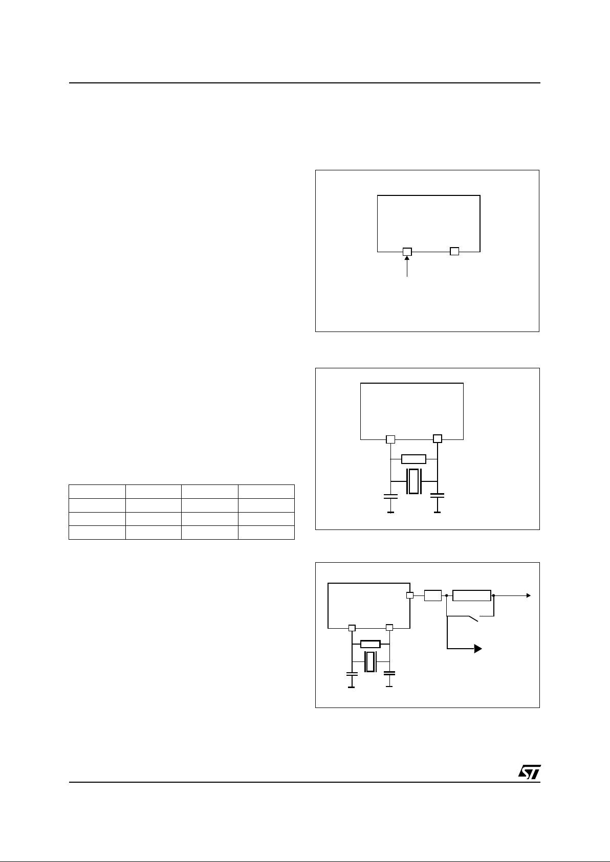
3.1.1 General Description
The MCU accepts either a Crystal or Ceramic resonator, or an external clock signal to drive the internal oscillator. The internal clock (f
CPU
) is de-
rived from the external os cillator frequency (f
OSC).
The external Oscillator clock is first divided by 2,
and an additional division factor of 2, 4, 8, o r 16
can be applied, in Slow Mode, to reduce the frequency of the f
CPU
; this clock signal is also routed
to the on-chip peripherals (except the CAN). The
CPU clock signal con si sts of a square wave with a
duty cycle of 50%.
The internal oscillat or is designed to operate with
an AT-cut parallel resonant quartz crystal resonator in the frequency range specified for f
osc
. The
circuit shown in Figure 5 is recommended when
using a crystal, and Tab le 2 lists the recommended capacitance and feedback resistance values.
The crystal and associated components should be
mounted as close as p ossible to the input pins i n
order to minimize output distortion and start-up
stabilisation time.
Use of an external CMOS oscillator is recommended when crystals outside the specified frequency ranges are to be used.
Table 2. Recommended Values for 16 MHz
Crystal Resonator
Note:
R
SMAX
is the equivalent serial resistor of the
crystal (see crystal specification).
C
OSCIN,COSCOUT
:
Maximum total capacitances on
pins OSCIN and OSCOUT (the value includes the
external capacitance tied to the p in plus the parasitic capacitance of the board and of the device).
Rp:
External shunt resistance. Recommended val-
ue for oscillat o r sta bility is 1MΩ.
Figure 4. External Clock Source Connections
Figure 5. Crystal/Ceramic Resonator
Figure 6. Clock Prescaler Block Diagram
R
SMAX
40
Ω
60
Ω
150
Ω
C
OSCIN
56pF 47pF 22pF
C
OSCOUT
56pF 47pF 22pF
R
P
1-10 MΩ 1-10 MΩ 1-10 MΩ
OSC
in
OSC
out
EXTERNAL
CLOCK
NC
OSC
in
OSC
out
C
OSCin
C
OSCout
R
P
OSC
in
OSC
out
C
OSCin
C
OSCout
R
P
%2 %2,4,8,16
CPUCLK
to CPU and
Peripherals
to CAN
Page 15
15/103
L9805
CLOCK SYSTEM
(Cont’d)
3.1.2 External Clock
An external clock may be applied to the OSCIN input with the OSCOUT pin not connected, as
shown on Figure 4. The t
OXOV
specifications does
not apply when usi ng an external clock input. T he
equivalent specification of the external clock
source should be used instead of t
OXOV
(see ).
Figure 7. Timing Diagram for Internal CPU Clock Frequency transitions
b1 : b2
MISCELLANEOUS REGISTER
00
01
b0
1
1
0
OSC/2
OSC/4
OSC/8
CPU CLK
VR02062B
New frequency
requested
New frequency
active when
osc/4 & osc/8 = 0
Normal mode active
(osc/4 - osc/8 stoppe
d
Normal mode
requested
Page 16

16/103
L9805
3.2 OSCILLATOR SAFEGUARD
The L9805 contains an oscilla tor safe guard function.
This function provides a real time check of the
crystal oscillator generating a reset condition when
the clock frequency has anomalous value.
If f
OSC<flow
, a reset is generated.
If f
OSC>fhigh,
a reset is generated.
A flag in the Dedicated Control Status Register indicates if the last reset is a safeguard reset.
At the output of reset state the safeguard is disable. To activate the safeguard SFGEN bit must be
set.
Notes:
Following a reset, the safeguard is disabled. Once activated it cannot be disabled, except
by a reset.
3.2.1 Dedicated Control Status Register
DCSR
Address 0022h - Read/Write
Reset Value:xx00 0000 (00h)
b6 =
SGFH:
Safeguard high flag. Set by an Oscillator Safeguard Reset generated for frequency too
high, cleared by software (writing zero) or Power
On / Low Voltage Reset. This flag is useful for distinguishing Safeguard Reset, Power On / Low
Voltage Reset and Watchdog Reset.
b7 =
SGFL:
Safeguard low flag. Set by an Oscillator Safeguard Reset generated for frequency too
low, cleared by software (writing zero) or Power
On / Low Voltage Reset. This flag is useful for distinguishing Safeguard Reset, Power On / Low
Voltage Reset and Watchdog Reset.
b5 =
SFGEN
: Safeguard enable when set. It’s
cleared only by hardware after a reset.
b4 =
CANDS
: CAN Transceiver disable. When this
bit is set the CAN transceiver goes in Power Down
Mode and does not work until this bit is reset.
CANDS is 0 after reset so the standard condition is
with the transceiver enabled. This bit can be used
by application requiring low power consumption
(see Section 5.7 for details).
b3,b2,b1 =
not used
b0 =
PIEN
: PWMI input enable. When set, the
PWMI input line is connected to Input Capture 2 of
Timer 2. Otherwise, ICAP2_2 is the alternate function of PA7. See Figure 31 for the explanation of
this function.
SGFL SGFH SFGEN CANDS
b3b2b
1
PIEN
Page 17
17/103
L9805
3.3 WATCHDOG SYSTEM (WDG)
3.3.1 Introd uct i on
The Watchdog is used to detect the occurrence of
a software fault, usually generated by external interference or by unforeseen logical conditions,
which causes the application program to give up its
normal sequence. The Watchdog circuit generates
an MCU reset on expiry of a programmed time period, unless the program re freshes the counter’s
contents before it is decremented to zero.
3.3.2 Main Features
– Programm able Time r (64 increments of 12,288
CPU clock)
– Programmable Reset
– reset (if watchdog activated) after an HALT in-
struction or when bit timer MSB reaches zero
– Watchdog Reset indicated by status flag.
3.3.3 Functional Description
The counter value stored in the CR register (bits
T6:T0), is decremented every 12,288 machine cycles, and the length of the timeout period can b e
programmed by the user in 64 increments.
If the watchdog is activated (the W DGA bit is s et)
and when the 7-bit timer (bits T6:T0) rolls over
from 40h to 3Fh (T6 becom es cleared), it initiates
a reset cycle pulling low the reset pin for typically
500ns.
The application program must write in the CR register at regular intervals during normal operation to
prevent an MCU reset. The value to be stored in
the CR register must be between FFh and C0h
(see Table 1):
– The WDGA bit is set (watchdog enabled)
– The T6 bit is set to prevent generating an imme-
diate reset
– The T5:T0 bit contain the number of increments
which represents the time delay before the
watchdog produces a reset.
Table 3. Wat chdog Timin g (f
OSC
= 16 MHz)
Notes:
Following a reset, the watchdog is disabled. Once activated it cannot be disabled, except
by a reset.
The T6 bit can be used to gen erate a s oftware reset (the WDGA bit is set and the T6 bit is cleared).
If the watchdog is activated, the HALT instruction
will generate a Reset.
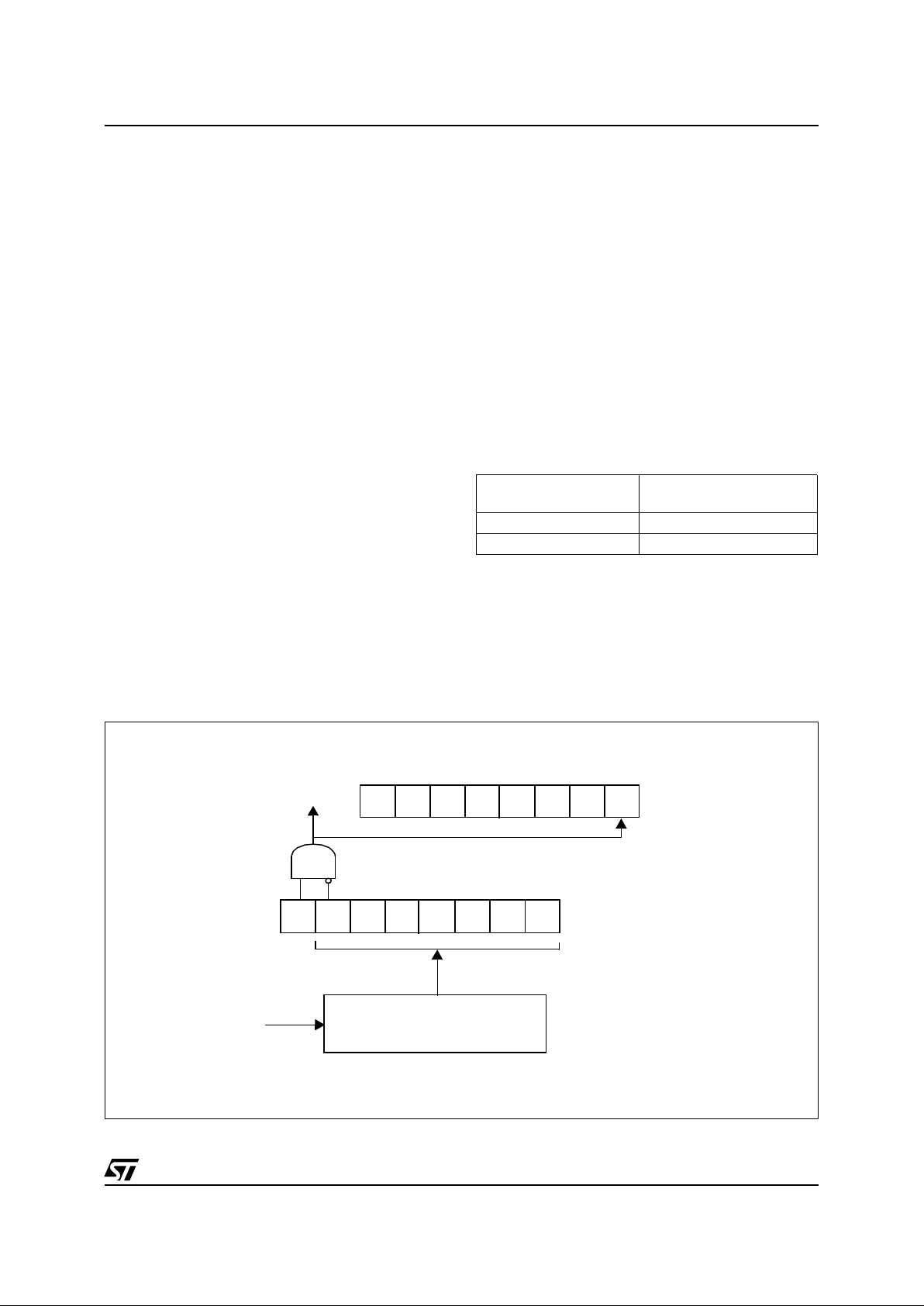
Figure 8. Functional Description
WDG Register initial
value
WDG timeout period (ms)
7Fh 98.3
C0h 1.54
RESET
WDGA
7-BIT DOWNCO UNTER
f
CPU
MSB LSB
CLOCK DIVIDE R
WDGF
WATCHDOG STATUS REGISTER (WDGSR)
WATCHDOG CONTROL REGIST ER (WDGCR)
÷12288
Page 18

18/103
L9805
WATCHDOG SY ST E M
(Cont’d)
The Watchdog delay time is defined by bi ts 5 -0 of
the Watchdog register; bit 6 must always be set in
order to avoid generating an immediate reset.
Conversely, this can be used to generate a software reset (bit 7 = 1, bit 6 = 0).
The Watchdog must be reloaded before bit 6 is decremented to “0” to avoid a Reset. F ollowing a Reset, the Watchdog register will contain 7Fh (bits 0-
7).
If the circuit is not used as a Watchdog (i.e. bit 7 is
never set), bits 6 to 0 ma y be u se d as a simple 7bit timer, for instance as a real t ime clock. Since no
reset will be generated under these conditions, the
Watchdog control register must be monitored by
softw are.
A flag in the watchdog status register indicates if
the last reset is a watchdog reset or not, before
clearing by a write of this register.
3.3.4 Register Description
3.3.4.1 Watchdog Control Register
(WDGCR)
Register Address: 002Ah — Read/Write
Reset Value: 0111 1111 (7Fh)
b7 =
WDGA:
Activation bit.
This bit is set by software and only cleared by
hardware after a reset. When WDGA = 1, the
watchdog can generate a reset.
0: Watchdog disabled
1: Watchdog enabled.
b6-0 =
T6-T0
: 7 bit timer (Msb to Lsb)
These bits contain the decremented value. A reset
is produced when it rolls over from 40h to 3Fh (T6
become cleared).
3.3.4.2 Watchdog Status Register
(WDGSR)
Register Address: 002Bh — Read/W rite
Reset Value
(*)
: 0000 0000 (00h)
b7-1 =
not used
b0 =
WDGF:
Watchdog flag. Set by a Watchdog
Reset, cleared by software (writing zero) or Power
On / Low Voltage Reset. This flag is useful for distinguishing Power On / Low Voltage Reset and
Watchdog Reset.
(*): Except in the case of Watchdog Reset.
70
WDGAT6T5T4T3T2T1T0
70
-------WDGF
Page 19
19/103
L9805
3.4 MISCELLANEOUS REGISTER
(MISCR)
The Miscellaneous register allows the user to select the Slow operating mode and to set the clock
division prescaler factor. Bits 3, 4 determine the
signal conditions which will trigger an interrupt request on I/O pins having interrupt capability.
Register Address: 0020h — Read/Write
Reset Value:0000 0000 (00h)
b0 -
Slow Mode Select
0- Normal mode - Oscillator frequency / 2
(Reset state)
1- Slow mode (Bits b1 and b2 define the prescaler
factor)
b1, b2 -
CPU clock prescaler for Slow Mode
The selection issued from b3/b4 combination is
applied to PA[0]..PA[7],PB0,PB1 external interrupt. The selection can be made only if I bit in CC
register is reset (interrupt enabled).
b3, b4 can be written only when the Interrupt Mask
(I) of the CC (Condition Code) register is set to 1.
b5,b6,b7 =
not used
b7 b6 b5 b4 b3 b2 b1 b0
b2 b1 Option
00
Oscillator frequency / 4
10
Oscillator frequency / 8
01
Oscillator frequency / 16
11
Oscillator frequency / 32
b4 b3 Option
00
Falling edge and low level (Reset state)
10
Falling edge only
01
Rising edge only
11
Rising and Falling edge
Page 20

20/103
L9805
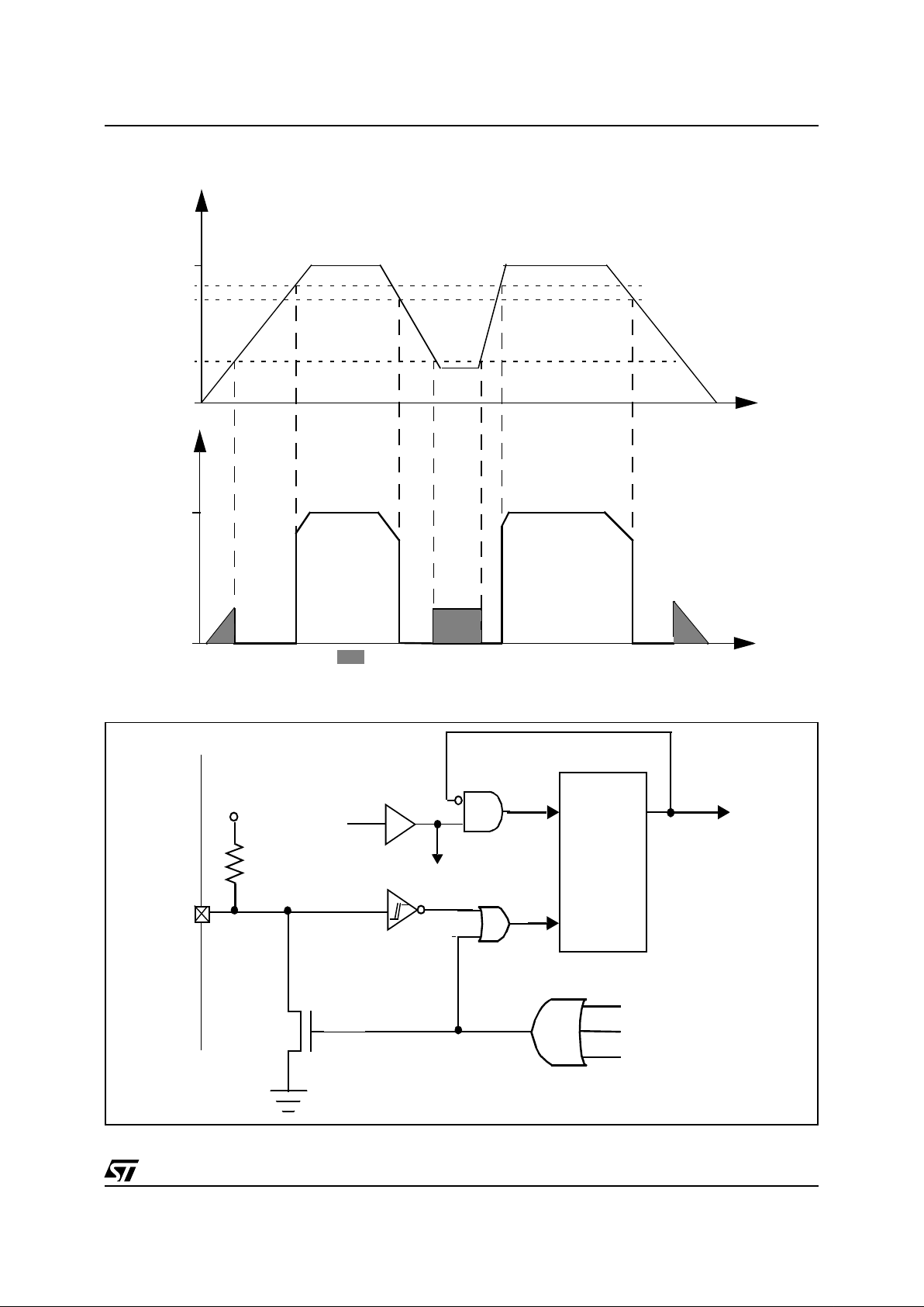
3.5 RESET
3.5.1 Introd uct i on
There are four sources of Reset:
– NRESET pin (external source)
– Power-On Reset / Low Voltage Detection (Inter-
nal source)
– WATCHDOG (Internal Source)
– SAFEGUARD (Internal source)
The Reset Service Routine vector is located at ad-
dress FFFEh-FFFFh.
3.5.2 External Reset
The NRESET pin is both an in put and an opendrain output with integrated pull-up resistor. When
one of the internal Reset sources is active, the Reset pin is driven low to reset the whole application.
3.5.3 Reset Operation
The duration of the Reset condition, which is also
reflected on the output pin, is fixed at 4096 internal
CPU Clock cycles. A Reset signal originating from
an external source must have a duration of at least
1.5 internal CPU Clock cycl es in order to b e recognised. At the end of the Power-On Reset cycle, the
MCU may be held in t he Reset condition by an External Reset signal. The NRESET pin may thus be
used to ensure V
DD
has risen to a point where the
MCU can operate correctly before the user program is run. Following a Power-On Reset event, or
after exiting Halt mode, a 409 6 CPU Clock cycle
delay period is initiated in order to allow the oscil-
lator to sta bilise and to ensu re that recovery ha s
taken place from the Reset state.
During the Reset cycle, the device Reset pin acts
as an output that is pulsed low. In i t s high state, an
internal pull-up resistor of about 300KΩ is connected to the Reset pin. This resistor can be pulled
low by external circuitry to reset the device.
3.5.4 Power-on Reset - Low Voltage Detection
The POR/LVD function generates a static reset
when the supply voltage is below a reference value. In this way, the Power-On Reset and Low Voltage Reset function are provided, in order to keep
the system in safe condition when the voltage is
too low.
The Power-Up and Power-Down thresholds are
different, in order to avoid spurious reset when the
MCU starts running and sinks current from the
supply.
The LVD reset circuitry generates a reset when
V
DD
is below:
– V
ResetON
when V
DD
is rising
– V
ResetOFF
when VDD is falling
The POR/LVD function is explained in Figure 9.
Power-On Reset activates the reset pull up tran-
sistor performing a complete chip reset. In the
same way a reset can be triggered by the watchdog, by the safeguard or by external low level at
NRESET pin. An external capacitor connected between NRESET and ground can extend the power
on reset period if required.
Page 21
21/103
L9805
Figure 9. Power Up/Down behaviour
Figure 10. Reset Block Diagram
= undefined value
5V
t
V
Reset UD
V
Reset OFF
V
Reset ON
5V
t
V
DD
POR/LVD
Internal
RESET
Oscillator
Signal
Counter
NRESET
to ST7
RESET
V
DD
Watchdog Reset
Safeguard Reset
POR/LVD Reset
300K
Reset
CLK
Page 22
22/103
L9805
3.6 INTERRUPTS
A list of interrupt sources is given in Table 4 below,
together with relevant details for each source. Interrupts are serviced according to t heir order of pri ority, starting with I0, which has the highest priority, and so to I12, which has the lowest priority.
The following list describes the origins for each interrupt lev el:
– I0 connected to Ports PA0-PA7, PB0-PB1
– I1 connected to CAN
– I2 connected to Power Diagnostics
– I3 connected to Output Compare of Timer 1
– I4 connected to Input Capture of TImer 1
– I5 connected to Timer 1 Overflow
– I6 connected to Output Compare of Timer 2
– I7 connected to Input Capture of TImer 2
– I8 connected to Time r 2 Overflow
– I9 connected to ADC End Of Conversion
– I10 connected to PWM 1 Overflow
– I11 connected to PWM 2 Overflow
– I12 connected to EEPROM
Exit from Halt mode may only be triggered by an
External Interrupt on one of the following ports:
PA0-PA7 (I0), PB0-PB1 (I0), or by an Internal Interrupt coming from CAN peripheral (I1).
If more than one input pin of a group connected to
the same interrupt line are selected simultaneously, the OR of this signals generates the interrupt.
Table 4. Interrupt Mapping
Interrupts Register Flag name
Interrupt
source
Vector
Address
Reset N/A N/A - FFFEh-FFFFh
Software N/A N/A - FFFCh-FFFDh
Ext. Interrupt (Ports PA0-PA7,
PB0-PB1)
N/A N/A I0 FFFAh-FFFBh
Receive Interrupt Flag
CAN Status
RXIFi
I1 FFF8h-FFF9hTransmit Interrupt Flag TXIF
Error Interrupt Pending EPND
Power Bridge Short Circuit
Bridge Control
Status
SC
I2 FFF6h-FFF7h
Overtemperature OVT
Output Compare 1
Timer 1 Status
OCF1_1
I3 FFF4h-FFF5h
Output Compare 2 OCF2_1
Input Capture 1
Timer 1 Status
ICF1_1
I4 FFF2h-FFF3h
Input Capture 2 ICF2_1
Timer Overflow Timer 1 Status TOF_1 I5 FFF0h-FFF1h
Output Compare 1
Timer 2 Status
OCF1_2
I6 FFEEh-FFEFh
Output Compare 2 OCF2_2
Input Capture 1
Timer 2 Status
ICF1_2
I7 FFECh-FFEDh
Input Capture 2 ICF2_2
Timer Overflow Timer 2 Status TOF_2 I8 FFEAh-FFEBh
ADC End Of Conversion ADC Control EOC I9 FFE8h-FFE9h
PWM 1 Overflow N/A N/A I10 FFE6h-FFE7h
PWM 2 Overflow N/A N/A I11 FFE4h-FFE5h
EEPROM Programming EEPROM Control E2ITE I12 FFE2h-FFE3h
Page 23
23/103
L9805
INTERRUPTS
(Cont’d)
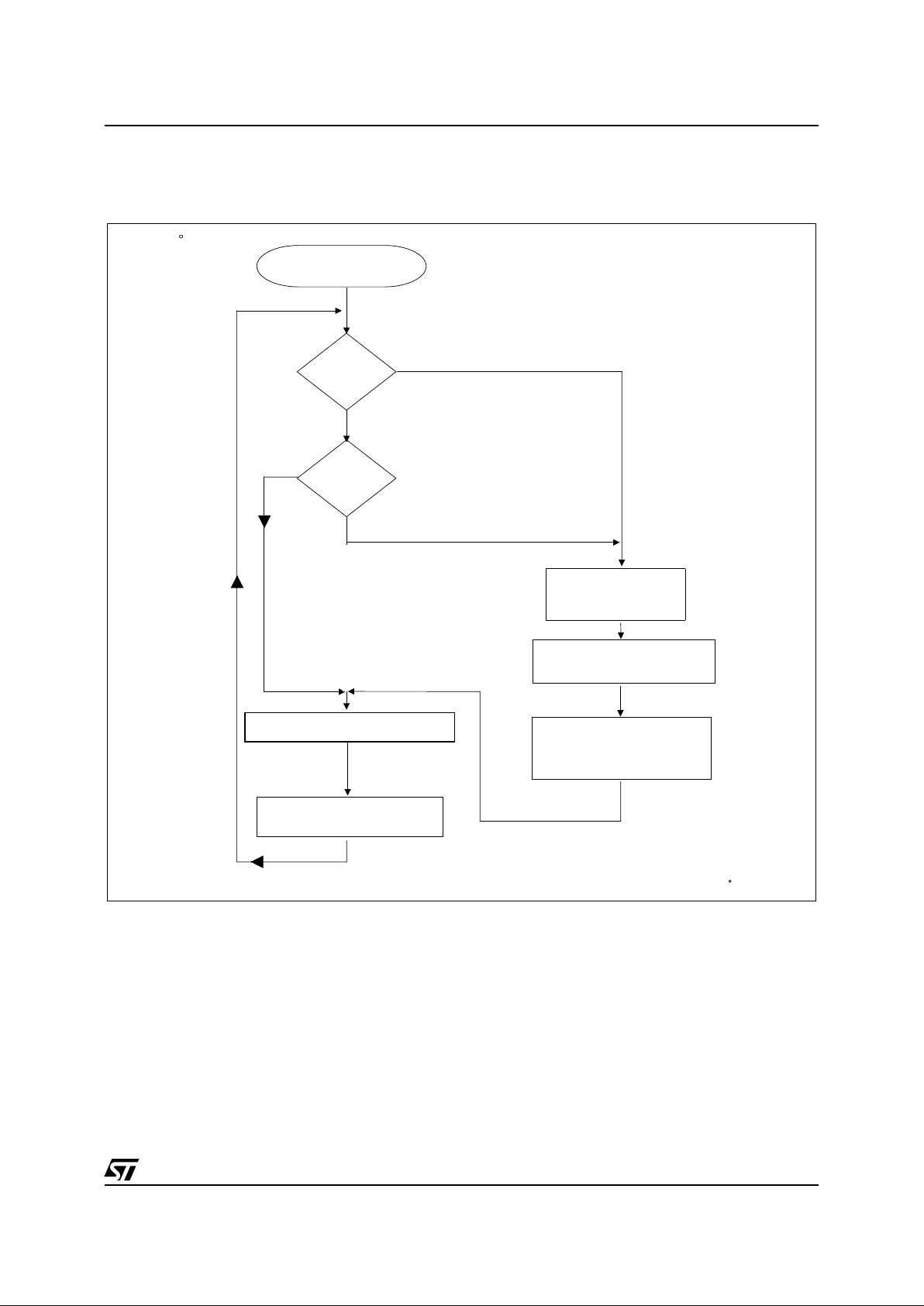
Figure 11. Inte rru pt P rocessing Flow c hart
Note
1. See Table 4
INTERRUPT
TRAP
FETCH NEXT
INSTRUCTION
OF APPROPRIATE INTERRUPT
SERVICE ROUTINE
EXECUTE INSTRUCTION
PUSH
PC,X,A,CC
SET I BIT TO 1
VR01172B
N
Y
LOAD PC
WITH APPROPRIATE
INTERRUPT VECTOR
(
1)
I BIT = 1
N
Y
ONTO STACK
Page 24
24/103
L9805
3.7 POWER SAVI NG MO DE S
3.7.1 Introd uct i on
There are three Power Saving modes. The Slow
Mode may be selected by setting the relevant bit s
in the Miscellaneous register as detailed in Section
3.4. Wait and Halt m odes may be entered usin g
the WFI and HALT instructions.
3.7.2 Slow Mode
In Slow mode, the oscillator frequency can be d ivided by 4, 8, 16 or 32 rathe r than by 2. The CP U
and peripherals (except CAN, see Note) are
clocked at this lower frequency. Slow mode is
used to reduce power consumption.
Note:
Before entering Slow mode and to guarantee low power operations, the CAN Controller
must be placed by software in STANDBY mode.
3.7.3 Wait Mode
Wait mode places the MCU in a low power consumption mode by stopping the CPU. All peripherals remain active. During Wait mode , the I bit (CC
Register) is cleared, so as to enabl e all interrupt s.
All other registers and memory remain unchanged. The MCU will remain in Wait m ode until
an Interrupt or Reset occurs, whereupon the Program Counter branches to t he starting address of
the Interrupt or Reset Service Routine.
The MCU will remain in Wait mode until a Reset or
an Interrupt (coming from CAN, Timers 1 & 2,
EEPROM, ADC, PWM 1 & 2, I/O ports peripherals
and Power Bridge) occurs, causing its wake-up.
Refer to Figure 12 below.
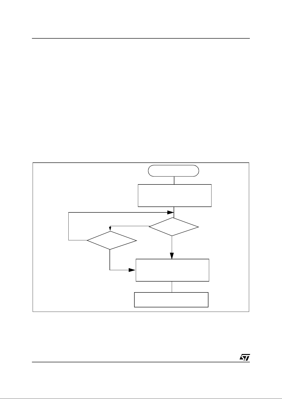
Figure 12. Wait Mode Flow Chart
WAIT INSTRUCTION
RESET
FETCH RESET VECTOR
OR SERVICE INTERRUPT
INTERRUPT
Y
N
N
Y
CPU CLOCK
OSCILLATOR
PERIPH. CLOCK
I-BIT
ON
ON
SET
ON
CPU CLOCK
OSCILLATOR
PERIPH. CLOCK
I-BIT
ON
ON
CLEARED
OFF
Page 25
25/103
L9805
POWER SAVING MODES
(Cont’d)
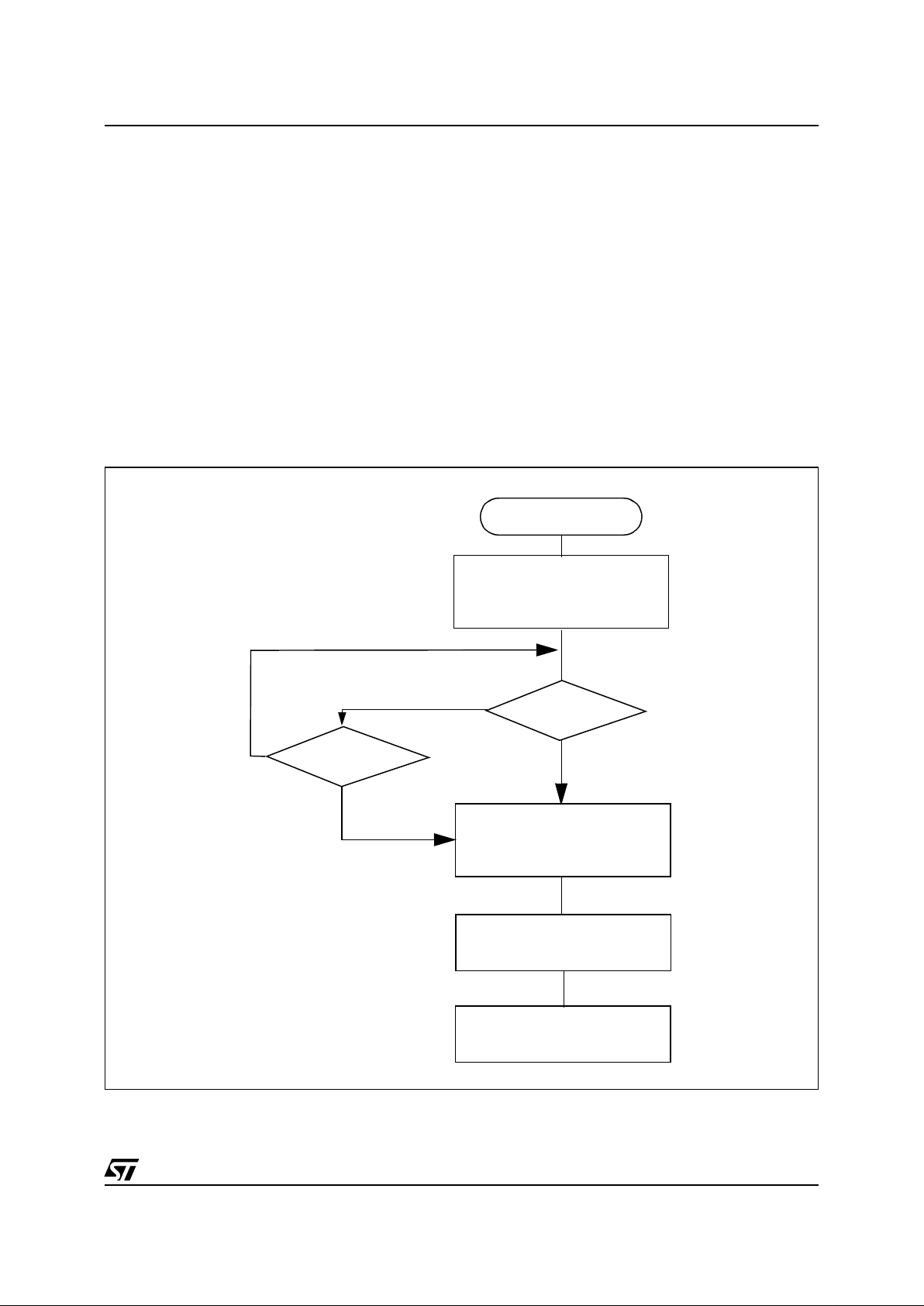
3.7.4 Halt Mode
The Halt mode is the MCU lowest power consumption mode. The Halt mode is entered by executing the HALT instruction. The internal oscillator
is then turned off, causing all internal processing to
be stopped, including the operation of the on-chip
peripherals.
When entering Halt mode, the I bit in the CC Register is cleared so as to enable External Interrupts.
If an interrupt occurs, the CPU becomes active.
The MCU can exit the Halt mode upon reception of
either an external interrupt (I0), a internal interrupt
coming from the CAN peripheral (I1) or a reset.
The oscillator is then turned on and a stabilisation
time is provided before releasing CPU operat ion.
The stabilisation time is 4096 CPU clock cycles.
After the start up delay, the CPU continues operation by servicing the interrupt which wakes it up or
by fetching the reset vector if a reset wakes it up.
Note
The Halt mode cannot be used when the
watchdog or the Safeguard are enabled, if the
HALT instruction is executed while the watchdog
or safeguard system are enabled, a reset is automatically generated thus resetting the entire MCU.
Note
Halt Mode affects o nly the digital section of
the device. All the analog circuit remain in their
status, including ADC, voltage regulators, bus
transceivers and power bridge.
Figure 13. Hal t Mode Flow Cha rt
N
N
EXTERNAL
INTERRUPT
RESET
HALT INSTRUCTION
4096 CPU CLOCK
FETCH RESET VECTOR
OR SERVICE INTERRUPT
CYCLES DELAY
CPU CLOCK
OSCILLATOR
PERIPH. CLOCK
I-BIT
ON
ON
SET
ON
CPU CLOCK
OSCILLATOR
PERIPH. CLOCK
I-BIT
OFF
OFF
CLEARED
OFF
Y
Y
Page 26
26/103
L9805
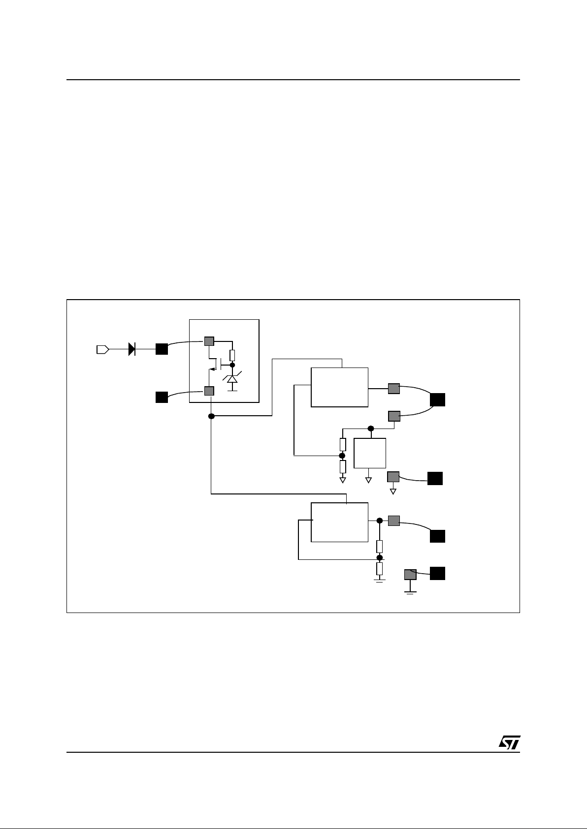
4 VOLTAGE REGULATO R
4.1 In troduc t ion
The on chip voltage regulator prov ides two regulated voltage, nominally 5V both. VCC supplies
ADC and the analog pe riphery and VDD supplies
the microcontroller and logic pa rts. These voltag e
are available at pins VDD and VCC to supply external components and c onnects a capacitors to
optimize EMI performance. A pre-regulator circuit
allows to connect external tantalum capacitors to a
lower (10V) voltage (VB2 pin).
4.1.1 Functional Description
The main supp ly v oltage is taken from V B 1 pin. A
voltage pre-regulator provides the regulated voltage on pin VB2. VB2 is the supply for the digital
and analog regulators. The bl ock diagram shows
the connections between the regulators and the
external pins.
In order to prevent negative spikes on the battery
line to propagate on the internal supply generating
spurious reset, a series diode suppl y VB1 pin is
recommended.
Figure 14. Vol ta ge regulation bl ock diagram
4.2 Digital Section Power Supply
The digital supply voltage VDD is available at pin
number 42 and 9. The digital ground GND is available at pin number 43 and 12.
Pin 42 and 43 are the actual voltage regulator output and external loads must be supply by these
pin. The 100nF compensation capacitor should be
connected as close as possible to pin 42 and 43.
Pin number 9 and 12 provide an external access to
the internal oscillator supply. Reson ator’s capacitors should be grounded on pin 12.
ADC
PRE-REGULATOR
VB1
VB2
force
ANALOG
VOLTAGE
REGULATOR
sense
VCC
AGND
DIGITAL
VOLTAGE
REGULATOR
VDD(42)
GND(43)
Battery
Page 27

27/103
L9805
The application board can improve noise reduction
in the chip connecting directly pin 42 to pin 9 and
pin 43 to pin 12 u sing trac es as short as possible.
An additional capacitor mounted close to pin 9 and
12 can lead additional improvement.
4.2.1 VDD Short Circuit Protection
The output current o f the digital voltage regulator
is controlled by a circuit that limits it to a maximum
value (I
MAXVDD
). When the output current exceeds
this value the VDD voltage starts falling down. External loads must be chosen taking in account this
maximum current capability of the regulator.
4.3 Analog Section Power Supply
The analog supply voltage is available on VCC
pin. The external 100nF com pensation capacitor
should be placed as close as possibl e to this pin
and AGND pin.
VCC is the reference voltage f or the AD conversion and must be used to s upply ratiometric sensors feeding AD inputs. Any voltage drop between
VCC pin and the sensor supply pin on the application board, will cause the ADC to be inaccurate
when reading the sensor’s output.
4.3.1 VCC Short Circuit Protection
The output current of th e anal og v oltage regulat or
is controlled by a circuit that limits it to a maximum
value (I
MAXVCC
). When the output current exceeds
this value the VCC voltage starts falling down. External loads must be chosen taking in account this
maximum current capability of the regulator.
WARNING: The pin VB2 i s not short circuit protected so a short circuit on this pin will destroy the
device.
Page 28

28/103
L9805
5 ON-CHIP PERIPHERALS
5.1 I/O PORTS
5.1.1 Introd uct i on
The internal I/O ports allow the transfer of data
through digital inputs and outputs, the interrupt
generation coming from an I/O and for specific
pins, the input/output of alternate signals for the
on-chip peripherals (TIMERS...).
Each pin can be programmed independently as
digital input (with or without interrupt generation)
or digital output.
5.1.2 Functional Description
Each I/O pin m ay be programmed indepen dently
as a digital input or a digital output, using the corresponding register bits.
Each port pin of the I/O Ports can be individual ly
configured under software control as either i nput
or output.
Each bit of a Data Direction Register (DDR) corresponds to an I/O pi n of the associated po rt. This
corresponding bit must be set to configure its associated pin as output and must be cleared to configure its associated pin as input. The Data Direction Registers can be read and written.
5.1.2.1 Input Mode
When DDR=0, the corresponding I/O is configured
in Input mode.
In this case, the output buffer is switched off, the
state of the I/O is readable through the Data Register address, but the I/O state comes directly from
the Schmitt-Trigger output and not from the Dat a
Register output.
5.1.2.2 Interrupt function
When an I/O is configured in Input with Interrupt
generation mode (DDR=0 and OR=1), a low level
or any transition on this I/O (according to the Miscellaneous register configuration - see Section
3.4, “b3, b4 External Interrupt Option”) will gener-
ate an Interrupt request to the CPU.
Each pin can independently generate an Interrupt
request. When at least one of the interrupt inp uts
is tied low, the port’s common interrupt will activate
a CPU interrupt input according to the e xternal interrupt option in the Miscellaneous Register.
5.1.2.3 Output Mode
When DDR=1, the corresponding I/O is configured
in Output mode. In this mode, the interrupt function
is disabled.
The output buffers c an be individually configured
as Open Drain or Push-Pull b y means of the Option Register.
The output buffer is activated according to the
Data Register’s content.
A read operation is directly performed from the
Data Register output.
5.1.2.4 Alternate function
A signal coming from a on-chip peripheral can be
output on the I/O.
In this case, the I/O is automaticall y configured in
output mode (without pull-up).
This must be controlled directly by the peripheral
with a signal coming from the peripheral which enables the alternate signal to be output.
The I/O’s state is readable as in normal mode by
addressing the corresponding I/O Data Register.
A signal coming from an I/O can be inpu t in a onchip peripheral.
Before using an I/O as Alternate Input, it must be
configured in Input without interrupt mode (DDR=0
and OR=0). So, bot h Alternat e In put co nfigurat ion
(with or without pull-up) and I/O input configuration
(with or without pull-up) are the same.
The signal to be input in the peripheral is taken after the Schmitt-trigger. The I/O’s state is reada ble
as in normal mode by address ing the corres ponding I/O Data Register.
Page 29
29/103
L9805
I/O PO R T S
(Cont’d)
5.1.2.5 I/O Port Implementation
The I/O port register configurations are resumed
as following.
Port PA(7:0), Port PB(2:0)
RESET status: DR=0, DDR=0 and OR=0 (Input
mode, no interrupt).
These ports offer interrupt capabilities.
5.1.2.6 Dedicated Configurations
Table 5. Port A Configuration
Table 6. Port B Configuration
DDR OR MODE
00
input
no interrupt (pull-up enabled)
01
input
interrupt (pull-up enabled)
1 0 Open-Drain output
1 1 Push-Pull output
PORT A
I / O Function
Input Output Alternate Interrupt
PA0 triggered with pull-up push-pull/open drain
OCMP2_1: Output Compare
#2 Timer 1
wake-up interrupt
(I0)
PA1 triggered with pull-up push-pull/open drain
OCMP1_1: Output Compare
#1 Timer 1
wake-up interrupt
(I0)
PA2 triggered with pull-up push-pull/open drain
ICAP2_1: Input Capture #2
Timer 1
wake-up interrupt
(I0)
PA3 triggered with pull-up push-pull/open drain
ICAP1_1: Input Capture #1
Timer 1
wake-up interrupt
(I0)
PA4 triggered with pull-up push-pull/open drain
EXTCLK_1: External Clock
Timer 1
wake-up interrupt
(I0)
PA5 triggered with pull-up push-pull/open drain
OCMP2_2: Output Compare
#2 Timer 2
wake-up interrupt
(I0)
PA6 triggered with pull-up push-pull/open drain
OCMP1_2: Output Compare
#1 Timer 2
wake-up interrupt
(I0)
PA7 triggered with pull-up push-pull/open drain
ICAP2_2: Input Capture #2
Timer 2
wake-up interrupt
(I0)
PORT B
I / O Function
Input Output Alternate Interrupt
PB0 triggered with pull-up push-pull/open drain
ICAP1_2: Input Capture #1
Timer 2
wake-up interrupt
(I0)
PB1 triggered with pull-up push-pull/open drain
EXTCLK_2: External Clock
Timer 2
wake-up interrupt
(I0)
PB2
1)
Note 1. The PB2 bit is not connected to the external. It must be configured as an Input without interrupt, to be used only as an alter nate
function.
Not connected to pad Not connected to pad PWMI: PWM input
Page 30
30/103
L9805
I/O PO R T S
(Cont’d)
Figure 15
.
Ports PA0-PA7, PB0-PB1
I
DR
DDR
latch
latch
Data Bus
DR SEL
DDR SEL
VDD
PAD
M
U
X
Alternate
Alternate
digital enable
Alternate enable
Alternate
M
U
X
Alternate inpu t
output
P-BUFFER
N-BUFFER
1
0
1
0
OR
latch
OR SEL
from
other
bits
Interrupt
Pull-up
condition
enable
enable
GND
Page 31

31/103
L9805
I/O PO R T S
(Cont’d)
5.1.3 Register Description
5.1.3.1 Data registers
(PADR)
Port A: 0000h
Read/Write
Reset Value: 0000 0000 (00h)
(PBDR)
Port B: 0004h
Read/Write
Reset Value: 0000 0000 (00h)
5.1.3.2 Data direction registers
(PADDR)
Port A: 0001h
Read/Write
Reset Value: 0000 0000 (00h) (input mode)
(PBDDR)
Port B: 0005h
Read/Write
Reset Value: 0000 0000 (00h) (input mode)
5.1.3.3 Option registers
(PAOR)
Port A: 0002h
Read/Write
Reset Value: 0000 0000 (00h) (no interrupt)
(PBOR)
Port B: 0006h
Read/Write
Reset Value: 0000 0000 (00h) (no interrupt)
70
MSB LSB
70
MSB 0 0 0 0 LSB
70
MSB LSB
70
MSB 0 0 0 0 LSB
70
MSB LSB
70
MSB 0 0 0 0 LSB
Page 32

32/103
L9805
5.2 16-BIT TIMER
5.2.1 Introd uct i on
The timer consists of a 16-bit free-running counter
driven by a programmable prescaler.
It may be used for a variety of purposes, including
pulse length measurement of up to two input signals (
input capture
) or generation of up to two out-
put waveforms (
output compare
and
PWM
).
Pulse lengths and waveform perio ds c an be m odulated from a few microseconds to several milliseconds using the timer prescaler and the CPU
clock prescaler.
5.2.2 Main Features
■
Programmable prescaler: f
cpu
divided by 2, 4 or 8.
■
Overflow status flag and maskable interrupt
■
External clock inpu t (must be at le ast 4 times
slower than the CPU
clock speed) with the choice
of active edge
■
Output compare functions with
– 2 dedicated 16-bit registers
– 2 dedicated programmable signals
– 2 dedicated status flags
– 1 dedicated maskable interrupt
■
Input capture functions with
– 2 dedicated 16-bit registers
– 2 dedicated active edge selection signals
– 2 dedicated status flags
– 1 dedicated maskable interrupt
■
Pulse width modulation mode (PWM)
■
One pulse mode
■
5 alternate functions on I/O ports
The Block Diagram is shown in Figure 16, on
page 33.
Note:
Some external pins are not available on all
devices. Refer to the device pin out description.
5.2.3 Functional Description
5.2.3.1 Counter
The principal block of the P rogrammable T imer is
a 16-bit free running counter and its associated
16-bit registers:
Counter Registers
– Counter High Register (CHR) is the most sig-
nificant byte (MSB).
– Counter Low Register (CLR) is the least sig-
nificant byte (LSB).
Alternate Counter Registers
– Alternate Count er Hi gh Regi ster ( ACHR) is th e
most significant byte (MSB).
– Alternate Counter Low Register (ACLR) is the
least significant byt e (LSB).
These two read-only 16-bit registers contain the
same value but with the difference that reading the
ACLR register does not clear the TOF bit (overflow
flag), (see note page 3).
Writing in the CLR register or ACLR register resets
the free running counter to the FFFCh value.
The timer clock depends on the cloc k control bits
of the CR2 register, as illu s t r ated in Table 7 Clock
Control Bits. The value in t he counter register re-
peats every 131.072, 262 .144 or 524.288 internal
processor clock cycles depending on the CC1 and
CC0 bits.
Page 33

33/103
L9805
16-BIT TIMER
(Cont’d)
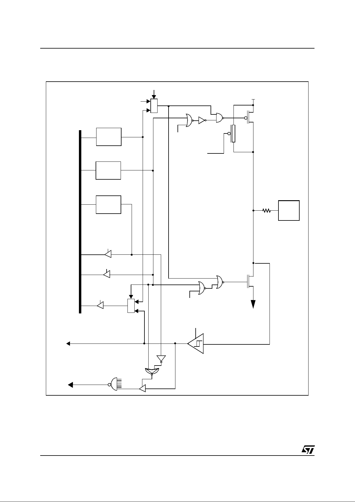
Figure 16. Timer Block Diagram
MCU-PERIPHERAL INTERFACE
COUNTER
ALTERNATE
REGISTER
OUTPUT
COMPARE
REGISTER
OUTPUT COMPARE
EDGE DETECT
OVERFLOW
DETECT
CIRCUIT
1/2
1/4
1/8
8-bit
buffer
ST7 INTERNAL BUS
LATCH1
OCMP1
ICAP1
EXCLK
CPU CLO CK
TIMER INTERRUPT
ICF2ICF1 000OCF2OCF1 TOF
PWMOC1E
EXEDG
IEDG2CC0CC1
OC2E
OPMFOLV2ICIE OLVL1IEDG1OLVL2FOLV1OCIETOIE
ICAP2
LATCH2
OCMP2
8
8
8 low
16
8 high
16 16
16
16
CR1
CR2
SR
6
16
8 8 8
88 8
high
low
high
high
high
low
low
low
EXEDG
TIMER INTERNAL BUS
CIRCUIT1
EDGE DETECT
CIRCUIT2
CIRCUIT
1
OUTPUT
COMPARE
REGISTER
2
INPUT
CAPTURE
REGISTER
1
INPUT
CAPTURE
REGISTER
2
CC1 CC0
16 BIT
FREE RUNNING
COUNTER
Page 34

34/103
L9805
16-BIT TIMER
(Cont’d)
16-bit read sequence:
(from either the Counter
Register or the Alternate Counter Register).
The user must read the MSB first, then the LSB
value is buffered automatically.
This buffered value rem ains unchanged until the
16-bit read sequence is completed, even if the
user reads the MSB several times.
After a complete reading sequence, if only the
CLR register or ACLR register are read, they return the LSB of the count value at the time of the
read.
An overflow occurs when the counter rolls over
from FFFFh to 0000h then:
– The TOF bit of the SR register is set.
– A timer interrupt is generated if:
– TOIE bit of the CR1register is set and
– I bit of the CCR register is cleared.
If one of these cond itions is false, the interrupt remains pending to be issued as soon as they are
both true.
Clearing the overflow interrupt request is done by:
1. Reading the SR register while the TOF bit is
set.
2. An access (read or write) to the CLR register.
Notes:
The TOF b it is not cleared by ac ces ses to
ACLR register. This feature allows simultaneous
use of the overflow f unction and rea ds of t he free
running counter at random times (for example, to
measure elapsed time) without the risk of clearing
the TOF bit erroneously.
The timer is not affected by WAIT mode.
In HALT mode, the counter stops counting until the
mode is exited. Count ing then resumes from the
previous count (MCU awakened by an interrupt) or
from the reset count (MCU awakened by a Reset).
5.2.3.2 External Clock
The external clock (wh ere available) is selected if
CC0=1 and CC1=1 in CR2 register.
The status of the EXEDG bit determi nes the type
of level transition on the external clock pin EXCLK
that will trigger the free running counter.
The counter is synchronised with t he falling edge
of the internal CPU clock.
At least four falling edges of the CPU clock must
occur between two consecutive active edges of
the external clock; thus the external clock frequency must be less than a quarter of the CPU clock
frequency.
LSB is buffered
Read MSB
At t0
Read LSB
Returns the buffered
LSB value at
t0
At t0 +∆t
Other
instructions
Beginning of the sequence
Sequence completed
Page 35

35/103
L9805
16-BIT TIMER
(Cont’d)
Figure 17. Counter Timing Diagram, internal clock divided by 2
Figure 18. Counter Timing Diagram, internal clock divided by 4
Figure 19. Counter Timing Diagram, internal clock divided by 8
CPU CLOCK
FFFD FFFE FFFF 0000 0001 0002 0003
INTERNAL RESET
TIMER CLOCK
COUNTER REGISTER
OVERFLOW FLAG TOF
FFFC FFFD 0000 0001
CPU CLOCK
INTERNAL RESET
TIMER CLOCK
COUNTER REGISTER
OVERFLOW FLAG TOF
CPU CLOCK
INTERNAL RESET
TIMER CLOCK
COUNTER REGISTER
OVERFLOW FLAG TOF
FFFC FFFD
0000
Page 36

36/103
L9805
16-BIT TIMER
(Cont’d)
5.2.3.3 Input Capture
In this section, the index,
i
, may be 1 or 2
The two input capture 16-bit registers (ICR1 and
ICR2) are used to latch the value of the free running counter after a transition detected by the
ICAP
i
pin (see figure 5).
ICR
i
register is a read-only register.
The active transition is software programmable
through the IEDG
i
bit of the Control Register (CRi).
Timing resolution is one count of the free running
counter: (
f
CPU/(CC1.CC0)
).
Procedure
To use the input capture function select the following in the CR2 register:
– Select the timer clock (CC1-CC0) (see Table 7
Clock Control Bits).
– Select the edge of the active transition on the
ICAP2 pin with the IEDG2 bit.
And select the following in the CR1 register:
– Set the ICI E bit to ge nerat e an in terrupt after an
input capture.
– Select the edge of the active transition on the
ICAP1 pin with the IEDG1 bit.
When an input capture occurs:
– ICF
i
bit is set.
– The ICR
i
register contai ns the value of the free
running counter on the active transition on the
ICAP
i
pin (see Figure 21).
– A timer interrupt is generated if the ICIE bit i s s e t
and the I bit is cleared in the CCR register. Otherwise, the interrupt remains pendi ng until both
conditions become true.
Clearing the Input Capture interrupt request is
done by:
1. Reading the SR register while the ICF
i
bit is set.
2. An access (read or write) to the ICLR
i
register.
Note:
After reading the ICHR
i
register, transfer of
input capture data is inhibited until the ICLR
i
regis-
ter is also read.
The ICR
i
register always contains the free running
counter value which corresponds to the most recent input capture.
During HALT mode, if at least one valid input capture edge occurs on the ICAP
i
pin, the input capture detection circuitry is armed. This does not set
any timer flags, and does not “wake-up” the MCU.
If the MCU is awoken by an interrupt, the input
capture flag will become active, and data corresponding to the first valid edge during HALT mode
will be present.
MS Byte LS Byte
ICR
i
ICHR
i
ICLR
i
Page 37

37/103
L9805
16-BIT TIMER
(Cont’d)
Figure 20. Input Capture Block Diagram
Figure 21. Input Capture Timing Diagram
ICIE
CC0
CC1
16-BIT
FREE RUNNING
COUNTER
IEDG1
(Control Register 1)
CR1
(Control Register 2)
CR2
ICF2ICF1 000
(Status Register) SR
IEDG2
ICAP1
ICAP2
EDGE DETECT
CIRCUIT2
16-BIT
ICR1
ICR2
EDGE DETECT
CIRCUIT1
FF01 FF02 FF03
FF03
TIMER CLOCK
COUNTER REGI STER
ICAPi PIN
ICAPi FLAG
ICAPi REGISTER
Note: A
ctive edge is rising edge.
Page 38

38/103
L9805
16-BIT TIMER
(Cont’d)
5.2.3.4 Output Compare
In this section, the index,
i
, may be 1 or 2.
This function can be used to control an output
waveform or indicating when a p eriod of time has
elapsed.
When a match is found bet ween the Output Compare register and the free running counter, the output compare function:
– Assigns pins with a programmable value if the
OCIE bit is set
– Sets a flag in the status register
– Generates an interrupt if enabled
Two 16-bit registers Output Compare Register 1
(OCR1) and Output Compare Register 2 (OCR2)
contain the value to be compared to the free running counter each timer clock cycle.
These registers are readable and writable and are
not affected by the timer hardware. A reset event
changes the OCRi value to 8000h.
Timing resolution is one count of the free running
counter: (
f
CPU/(CC1.CC0)
).
Procedure
To use the output compare function, select the following in the CR2 register:
– Set the O C
i
E bit if an output is needed then the
OCMP
i
pin is dedicated to the output com pare
i
function.
– Select the timer clock (CC1-CC0) (see Table 7
Clock Control Bits).
And select the following in the CR1 register:
– Select the OLVL
i
bit to applied to the OCMPi pins
after the match occurs.
– Set the OCIE bit to generate an interrupt i f it is
needed.
When match is found:
– OC F
i
bit is set.
– The OCMP
i
pin takes OLVLi bit value (OCMPi
pin latch is forced low during reset and stays low
until valid compares change it to a high level).
– A timer interrupt is generated if the OCIE bit is
set in the CR2 register and the I bit is cleared in
the CCR register (CCR).
Clearing the output compare interrupt request is
done by:
3. Reading the SR register while the OCF
i
bit is
set.
4. An access (read or write) to the OCLR
i
register.
Note:
After a processor write cycle to the OCHR
i
register, the output compare function is inh ibited
until the OCLR
i
register is also written.
If the OC
i
E bit is not set, the OCMPi pin is a gen-
eral I/O port and the OLVL
i
bit will not appear
when match is found but an interrupt could be generated if the OCIE bit is set.
The value in the 16-bit OCR
i
register and the OLV
i
bit should be changed after each successful comparison in order to control an o utput waveform or
establish a new elapsed timeout.
The OCR
i
register value required for a specific timing application can be c alcul ated using the following f ormula:
Where:
t = Desired output compare period (in
seconds calculated from the current
counter)
f
CPU
= Internal clock frequency (see Miscel-
laneous register)
CC1-CC0 = Timer clock prescaler
The following procedure is recommended to pre-
vent the OCF
i
bit from being set between the time
it is read and the write to the OCR
i
register:
– Write to the OCHR
i
register (further compares
are inhibited).
– Read the SR register (first step of the clearance
of the OCF
i
bit, which may be already set).
– Write to the OCLR
i
register (enables the output
compare function and clears the OCF
i
bit).
MS Byte LS Byte
OCR
i
OCHR
i
OCLR
i
∆
OCRi register Value =
t * f
CPU
(CC1.CC0)
Page 39

39/103
L9805
16-BIT TIMER
(Cont’d)
Figure 22. Output Compare Block Diagram
Figure 23. Output Compare Timing Diagram, Internal Clock Divided by 2
OUTPUT COMPARE
16-bit
CIRCUIT
OCR1
16 BIT FREE RUNNING
COUNTER
OC1E CC0CC1
OC2E
OLVL1OLVL2OCIE
(Control Register 1)
CR1
(Control Register 2)
CR2
000OCF2OCF1
(Status Register)
SR
16-bit
16-bit
OCMP1
OCMP2
Latch
1
Latch
2
OCR2
INTERNAL CPU CLOCK
TIMER CLOCK
COUNTER
OUTPUT COMPARE REGISTER
COMPARE REGISTER LATCH
OCFi AND OCMPi PIN (OLVLi=1)
CPU
writes
FFFF
FFFF
FFFD FFFD FFFE
FFFF
0000FFFC
Page 40

40/103
L9805
16-BIT TIMER
(Cont’d)
5.2.3.5 Forced Compare Mode
In this section
i
may represent 1 or 2.
The main purpose of the Forced Compare mode is
to easily generate a fixed frequency.
The following bits of the CR1 register are used:
When the FOLV
i
bit is set, the OLV Li bit is copied
to the OCMP
i
pin.
To provide this capability, internal logic allows a
single instruction to change the OLVL
i
bit and
causes a forced compare with the new value of the
OLVL
i
bit.
The OCF
i
bit is not set, and t hus no interrupt re-
quest is generated.
5.2.3.6 One Pulse Mode
One Pulse mode enables the generation of a
pulse when an external event occurs. This mode is
selected via the OPM bit in the CR2 register.
The one pulse mode uses the Input Capture1
function and the Output Compare1 function.
Procedure
To use one pulse mode, select the following in the
CR1 register:
– Using the OLVL1 bit, select the level to be ap-
plied to the OCMP1 pin after the pulse.
– Using the OLVL2 bit, select the level to be ap-
plied to the OCMP1 pin during the pulse.
– Select the edge of the active transition on the
ICAP1 pin with the IEDG1 bit
.
– Set OC1E pin, the OCMP1 pin is then dedicated
to the Output Compare 1 function.
And select the following in the CR2 register:
– Set the OPM bit.
– Select the timer clock CC1-CC0 (see Table 7
Clock Control Bits).
Load the OCR1 register with the value corresponding to the length of the pulse (see the formula in Section 5.2.3.7).
Then, on a valid event on the ICAP1 pin, the counter is initialized to FFFCh and OLVL2 bit is loaded
on the OCMP1 pin. When the value of the counter
is equal to the value o f the cont ents o f the OCR1
register, the OLVL1 bit i s output on the OCMP1
pin, (See Figure 24).
Note:
The OCF1 bit cannot be set by hardwa re in
one pulse mode but the OCF2 bit can generate an
Output Compare interrupt.
The ICF1 bit is set when an ac tive edge occurs
and can generate an interrupt if the ICIE bit is set.
When the Pulse Width Modulation (PWM) and
One Pulse Mode (OPM) bits are both set, the
PWM mode is the only active one.
Figure 24.
One
Pulse Mode Timing
FOLV2FOLV1OLVL
2
OLVL
1
event occurs
Counter is
initialized
to FFFCh
OCMP1 = OLVL2
Counter
= OCR1
OCMP1 = OLVL1
When
When
on ICAP1
One pulse mode cycle
COUNTER
....
FFFC FFFD FFFE 2ED0 2ED1 2ED2
2ED3
FFFC FFFD
OLVL2
OLVL2OLVL1
ICAP1
OCMP1
compare1
Note:
IEDG1=1, OCR1=2ED0h, OLVL1=0, OLVL2=1
Page 41

41/103
L9805
16-BIT TIMER
(Cont’d)
5.2.3.7 Pulse Width Modulation Mode
Pulse Width Modulation mode enables the generation of a signal with a frequency and pulse length
determined by the valu e of the OCR1 and OCR2
registers.
The pulse width modulation mode uses the complete Output Compare 1 funct ion plus the OCR2
register.
Procedure
To use pulse width modulation mode select the following in the CR1 register:
– Using the O LVL1 bit, select the level to be ap-
plied to the OCMP1 pin after a successful comparison with OCR1 register.
– Using the O LVL2 bit, select the level to be ap-
plied to the OCMP1 pin after a successful comparison with OCR2 register.
– Set OC1E bit : the OCM P 1 pin is then dedicated
to the output compare 1 function.
And select the following in the CR2 register:
– Set the PWM bit.
– Select the timer clock (CC1-CC0) (see Table 7
Clock Control Bits).
Load the OCR2 register with the value corresponding to the period of the signal.
Load the OCR1 register with the value corresponding to the length of the pulse i f (OLVL1=0
and OLVL2=1).
If OLVL1=1 and OLVL 2=0 the l ength o f the pul se
is the difference between the OCR2 and OCR1
registers.
The OCR
i
register value required for a specific timing application can be calculated using the following formula:
Where:
– t = Desired output compare period (seconds)
–f
CPU
= Internal clock frequency (see Miscella-
neous register)
– CC1-CC0 = Timer clock prescaler
The Output Compare 2 event causes the counter
to be initialized to FFFCh (See Figure 25, on
page 42).
Note:
After a write instruction to the OCHR
i
register, the output compare function is inhibited until
the OCLR
i
register is also written.
The OCF1 and OCF2 bits cannot be set by hardware in PWM mode therefore the Output Compare
interrupt is inhibited. The Input Capture interrupt is
available.
When the Pulse Width Modulation (PWM) and
One Pulse Mode (OPM) bits are both set, the
PWM mode is the only active one.
OCR
i
Value =
t * f
CPU
(CC1.CC0)
- 5
Counter
Counter is reset
to FFFCh
OCMP1 = OLVL 2
Counter
= OCR2
OCMP1 = OLVL1
When
When
= OCR1
Pulse Width Modulation cycle
Page 42

42/103
L9805
Figure 25. Pul s e W i dth Modulat io n Mo de Ti m in g
COUNTER
34E2
FFFC FFFD FFFE 2ED0 2ED1 2ED2 34E2 FFFC
OLVL2
OLVL2OLVL1
OCMP1
compare2 compare1 compare2
Note:
OCR1=2ED0h, OCR2=34E2, OLV L1= 0, OLVL2= 1
Page 43

43/103
L9805
16-BIT TIMER
(Cont’d)
5.2.4 Register Description
Each Timer is associated with three control and
status registers, and with six pairs of data registers
(16-bit values) relating to the two input captures,
the two output compares, the count er and the a lternate counter.
CONTROL REGISTER 1 (CR1)
Timer1 Register Address: 0032h
Timer2 Register Address: 0042h
Read/Write
Reset Value: 0000 0000 (00h)
Bit 7 =
ICIE
Input Capture Interrupt Enable.
0: Interrupt is inhibited.
1: A timer interrupt is generated whenever the
ICF1 or ICF2 bits of the SR register are set
Bit 6 =
OCIE
Output Compare Interrupt Enable.
0: Interrupt is inhibited.
1: A timer interrupt is generated whenever the
OCF1 or OCF2 bits of the SR register are set
Bit 5 =
TOIE
Timer Overflow Interrupt Enable.
0: Interrupt is inhibited.
1: A timer interrupt is enabled whenever the TOF
bit of the SR register is set.
Bit 4 =
FOLV2
Forced Output Compare 2.
0: No effect.
1:Forces the OLVL2 bit to be copied to the
OCMP2 pin.
Bit 3 =
FOLV1
Forced Output Compare 1.
0: No effect.
1: Forces OLVL1 to be copied to the OCMP1 pin.
Bit 2 =
OLVL2
Output Level 2.
This bit is copied to the OCMP2 pin whenev er a
successful compa rison occurs with t h e OCR2 register. This value is copied to the OCMP1 pin in
One Pulse Mode and Pulse Width Modulation
mode.
Bit 1 =
IEDG1
Input Edge 1.
This bit determines wh ich type of level transition
on the ICAP1 pin will trigger the capture.
0: A falling edge triggers the capture.
1: A rising edge triggers the capture.
Bit 0 =
OLVL1
Output Level 1.
The OLVL1 bi t is c opied to t he OCMP1 pin whenever a successful comparison occurs with the
OCR1 register.
70
ICIE OCIE TOIE
FOLV2FOLV1OLVL2IEDG1OLVL
1
Page 44

44/103
L9805
16-BIT TIMER
(Cont’d)
CONTROL REGISTER 2 (CR2)
Timer1 Register Address: 0031h
Timer2 Register Address: 0041h
Read/Write
Reset Value: 0000 0000 (00h)
Bit 7 =
OC1E
Output Compare 1 Enable.
0: Output Compare 1 function is ena bled, but th e
OCMP1 pin is a general I/O.
1: Output Compare 1 function is enabled, the
OCMP1 pin is dedicated to the Output Compare
1 capability of the timer.
Bit 6 =
OC2E
Output Compare 2 Enable.
0: Output Compare 2 function is ena bled, but th e
OCMP2 pin is a general I/O.
1: Output Compare 2 function is enabled, the
OCMP2 pin is dedicated to the Output Compare
2 capability of the timer.
Bit 5 =
OPM
One Pulse Mode.
0: One Pulse Mode is not active.
1: One Pulse M ode is act ive, the ICAP1 pin can be
used to trigger one pulse on the OCMP1 pin; the
active transition is g iven by the I EDG1 bit. Th e
length of the generated pulse depends on the
contents of the OCR1 register.
Bit 4 =
PWM
Pulse Width Modulation.
0: PWM mode is not active.
1: PWM mode is active, the OCMP1 pin out puts a
programmable cyclic signal; the length of the
pulse depends on the value of OCR1 register;
the period depends on the value of OCR2 register.
Bit 3, 2 =
CC1-CC0
Clock Control.
The value of the timer clock depends on these bits:
Table 7. Clock Control Bits
Bit 1 =
IEDG2
Input Edge 2.
This bit determines wh ich type of level transition
on the ICAP2 pin will trigger the capture
0: A falling edge triggers the capture.
1: A rising edge triggers the capture.
Bit 0 =
EXEDG
External Clock Edge.
This bit determines wh ich type of level transition
on the external clock pin EXCLK will trigger the
free running counter.
0: A falling edge triggers the free running counter.
1: A rising edge triggers the free running counter.
70
OC1E OC2E OPM PWM CC1 CC0 IE DG2 EXEDG
CC1 CC0 Timer Clock
00
f
CPU
/ 4
01
f
CPU
/ 2
10
f
CPU
/ 8
11
External Clock (where
available)
Page 45

45/103
L9805
16-BIT TIMER
(Cont’d)
STATUS REGISTER (SR)
Timer1 Register Address: 0033h
Timer2 Register Address: 0043h
Read Only
Reset Value: 0000 0000 (00h)
The three least significant bits are not used.
Bit 7 =
ICF1
Input Capture Flag 1.
0: No input capture (reset value)
1: An input capture has occurred. To clear this bit,
first read the SR register, then read or write the
low byte of the ICR1 (ICLR1) register.
Bit 6 =
OCF1
Output Compare Flag 1.
0: No match (reset value)
1: The content of the free running counter has
matched the content of the OCR1 register. To
clear this bit, first read the SR register, t hen read
or write the low byte of the OCR1 (OCLR1) register.
Bit 5 =
TOF
Timer Ov erflow.
0: No timer overflow (reset value)
1:The free running counter rolled over from FFFFh
to 0000h. To clear this bit, first read the SR register, then read or write the low byte of the CR
(CLR) register.
Note:
Reading or writing the ACLR register do not
clea r TOF.
Bit 4 =
ICF2
Input Capture Flag 2.
0: No input capture (reset value)
1: An input capture has occurred.To c lear this bit,
first read the SR register, then read or write the
low byte of the ICR2 (ICLR2) register.
Bit 3 =
OCF2
Output Compare Flag 2.
0: No match (reset value)
1: The content of the free running counter has
matched the cont ent of the OCR2 register. To
clear this bit, first read the SR register, then read
or write the low byte of the OCR2 (OCLR2) register.
Bit 2-0 = Unused.
70
ICF1 OC F1 TOF ICF2 OCF 2
Page 46

46/103
L9805
16-BIT TIMER
(Cont’d)
INPUT CAPTURE 1 HIGH REGISTER (ICHR1)
Timer1 Register Address: 0034h
Timer2 Register Address: 0044h
Read Only
Reset Value: Undefined
This is an 8-bit read only register that contains the
high part of the counter value (transferred by the
input capture 1 event).
INPUT CAPTURE 1 LOW REGISTER (ICLR1)
Timer1 Register Address: 0035h
Timer2 Register Address: 0045h
Read Only
Reset Value: Undefined
This is an 8-bit read only register that contains the
low part of the counter value (transferred by the input capture 1 event).
OUTPUT COMPARE 1 HIGH REGISTER
(OCHR1)
Timer1 Register Address: 0036h
Timer2 Register Address: 0046h
Read/Write
Reset Value: 1000 0000 (80h)
This is an 8-bit register that cont ains the high part
of the value to be compared to the CHR register.
OUTPUT COMPARE 1 LOW REGISTER
(OCLR1)
Timer1 Register Address: 0037h
Timer2 Register Address: 0047h
Read/Write
Reset Value: 0000 0000 (00h)
This is an 8-bit register that contains the low part of
OUTPUT COMPARE 2 HIGH REGISTER
(OCHR2)
Timer1 Register Address: 003Eh
Timer2 Register Address: 004Eh
Read/Write
Reset Value: 1000 0000 (80h)
This is an 8-bit re gister tha t co ntains t he hi gh part
of the value to be compared to the CHR register.
OUTPUT COMPARE 2 LOW REGISTER
(OCLR2)
Timer1 Register Address: 003Fh
Timer2 Register Address: 004Fh
Read/Write
Reset Value: 0000 0000 (00h)
This is an 8-bit register that contains the low part of
the value to be compared to the CLR register.
COUNTER HIGH REGISTER (CHR)
Timer1 Register Address: 0038h
Timer2 Register Address: 0048h
Read Only
Reset Value: 1111 1111 (FFh)
This is an 8-bit re gister tha t co ntains t he hi gh part
of the counter value.
70
MSB LSB
70
MSB LSB
70
MSB LSB
70
MSB LSB
70
MSB LSB
70
MSB LSB
70
MSB LSB
Page 47

47/103
L9805
COUNTER LOW REGISTER (CLR)
Timer1 Register Address: 0039h
Timer2 Register Address: 0049h
Read/Write
Reset Value: 1111 1100 (FCh)
This is an 8-bit register that contains the low part of
the counter value. A write to this register resets the
counter. An access to this register after accessing
the SR register clears the TOF bit.16-BIT
ALTERNATE COUNTER HIGH REGISTER
(ACHR)
Timer1 Register Address: 003Ah
Timer2 Register Address: 004Ah
Read Only
Reset Value: 1111 1111 (FFh)
This is an 8-bit register that cont ains the high part
of the counter value.
ALTERNATE COUNTER LOW REGISTER
(ACLR)
Timer1 Register Address: 003Bh
Timer2 Register Address: 004Bh
Read/Write
Reset Value: 1111 1100 (FCh)
This is an 8-bit register that contains the low part of
the counter value. A write to this register resets the
counter. An access to this register after an access
to SR register does no t clear the TOF bit i n SR
register.
INPUT CAPTURE 2 HIGH REGISTER (ICHR2)
Timer1 Register Address: 003Ch
Timer2 Register Address: 004Ch
Read Only
Reset Value: Undefined
This is an 8-bit read only register that contains the
high part of the counter value (transferred by the
Input Capture 2 event).
INPUT CAPTURE 2 LOW REGISTER (ICLR2)
Timer1 Register Address: 003Dh
Timer2 Register Address: 004Dh
Read Only
Reset Value: Undefined
This is an 8-bit read only register that contains the
low part of the counter value (transferred by the Input Capture 2 event).
70
MSB LSB
70
MSB LSB
70
MSB LSB
70
MSB LSB
70
MSB LSB
Page 48

48/103
L9805
16-BIT TIMER
(Cont’d)
Table 8. 16-Bit Timer Register Map and Reset Values
Address
(Hex.)
Register
Name
76543210
Timer1: 32
Timer2: 42
CR1
Reset Value
ICIE
0
OCIE
0
TOIE0FOLV20FOLV10OLVL20IEDG10OLVL1
0
Timer1: 31
Timer2: 41
CR2
Reset Value
OC1E0OC2E
0
OPM
0
PWM
0
CC1
0
CC0
0
IEDG20EXEDG
0
Timer1: 33
Timer2: 43SRReset Value
ICF1
0
OCF1
0
TOF
0
ICF2
0
OCF2
0
-
0
-
0
-
0
Timer1: 34
Timer2: 44
ICHR1
Reset Value
MSB
-
------
LSB
-
Timer1: 35
Timer2: 45
ICLR1
Reset Value
MSB
-
------
LSB
-
Timer1: 36
Timer2: 46
OCHR1
Reset Value
MSB
-
------
LSB
-
Timer1: 37
Timer2: 47
OCLR1
Reset Value
MSB
-
------
LSB
-
Timer1: 3E
Timer2: 4E
OCHR2
Reset Value
MSB
-
------
LSB
-
Timer1: 3F
Timer2: 4F
OCLR2
Reset Value
MSB
-
------
LSB
-
Timer1: 38
Timer2: 48
CHR
Reset Value
MSB
1111111
LSB
1
Timer1: 39
Timer2: 49
CLR
Reset Value
MSB
1111110
LSB
0
Timer1: 3A
Timer2: 4A
ACHR
Reset Value
MSB
1111111
LSB
1
Timer1: 3B
Timer2: 4B
ACLR
Reset Value
MSB
1111110
LSB
0
Timer1: 3C
Timer2: 4C
ICHR2
Reset Value
MSB
-
------
LSB
-
Timer1: 3D
Timer2: 4D
ICLR2
Reset Value
MSB
-
------
LSB
-
Page 49

49/103
L9805
5.3 PWM GENERATOR
5.3.1 Introd uct i on
This PWM peripheral includes a 16-bit Pulse
Width Modulator (PWM) and a programmable
prescaler able to generate an internal clock with
period as long as 128*T
CPU
.
The repetition rate of the 16-Bit PWM output can
be defined by a dedicated register (f
CPU
/CYREG);
its resolution is defined by the internal clock as per
the prescaler programming.
Main Features
-Programmable prescaler: f
CPU
divided by 2, 4, 8,
16, 32, 64 or 128.
-1 control register
-2 dedicated 16-bit registers for cycle and duty
control
-1 dedicated maskable interrupt
Procedure
To use the pulse width modulation peri pheral, the
EN_PWM bit in CONREG register must be set.
Load PS(2:0) in CONREG register to define the
programmable prescaler.
Load the CYREG register with the value defining
the cycle length (in internal clock periods). The 16
bits of this register are separated in two registers:
CYREGH and CYREGL.
Load the DUTYREG register with the value corresponding to the pulse length (in internal cycle periods). The 16 bits of this registe r are separated in
two registers: DUTYREGH and DUTYREGL.
The counter is reset to zero when EN_PWM bit is
reset.
Writing the DUTYREG and CYREG registers has
no effect on the current PWM cycle. The c ycle or
duty cycle change take place only after the first
overflow of the counter.
The suggested procedures to change the PWM
parameters are the following:
Duty Cycle control:
- Write the low and high DUTYREG registers.
A writing only on one DUTYREG register has no
effect until both registers are written.
The current PWM cycle will be completed. The
new duty cycle will be effective at the following
PWM cycle, with respect to the last DUTYREG
writing.
Cycle control:
- Write the low and high CYREG register
A writing only on o ne CYREG register has no effect until both registers are written.
The current PWM cycle will be completed. The
new cycle will be e ffective at the following PWM
cycle, with respect to the last CYREG writing.
Another possible procedure is:
- Reset the EN_PWM bit.
- Write the wanted configuration in CYREG and
DUTYREG..
- Set the EN_PWM bit.
If the EN_PWM bit is set after being reset, the cur-
rent values of DUTYREG and CYREG are determining the output waveform, no matter if only the
low or the high part, or both were written.
The first time EN_PWM is set, if CYREG and DUTYREG were not previously written, the output is
permanently low, because the default value of the
registers is 00h.
Changing the Prescaler ratio writing PS(2:0) in
CONREG has imm ediate effect on the waveform
frequency.
5.3.2 Functional Description
The PWM modul e consists of a 16-bit count er, a
comparator and the cycle generation logic.
PWM Generat ion
The counter increments continuously, clocked at
internal clock generated by prescaler. Whenever
the 16 bits of the counter (defined as the PWM
counter) overflow, the output level is set. The overflow value is defined by CYREG register.
The state of the PWM counter is continuously
compared to the PWM binary weight, as defined in
DUTYREG register, and when a match occurs the
output level is reset.
Figure 26. PWM Cycle
Note:
If the CYREG value is minor or equal than
DUTYREG value, PWM output remains set . With a
Counter
Counter is reset
OUT PWM = 1
Counter
= CYREG
OUT PWM = 0
When
When
= DUTYREG
Pulse Width Modulation cycle
Page 50

50/103
L9805
DUTYREG value of 0000h, the PWM output is permanently at low level, no matter of the value of
CYREG. With a DUTYRE G value of FFFFh, the
PWM output is permanently at high level.
Interrupt Request
The EN_INT bit i n CONREG register m ust be set
to enable the interrupt generation. When the 16
bits of the counter roll-over CYCLE RE G val ue, interrupt request is set.
The interrupt request is cleared whe n any of the
PWM registers is written.
Figure 27. PWM Generation
COUNTER
CYREG
COMPARE
VALUE
000
t
PWM OUTPUT
t
T
(INTERNAL CLOCK)
x Cyreg_value
value
Interrupt Generation
Page 51

51/103
L9805
5.3.3 Register Description
The PWM is associated with a 8-bit control registers, and with two 16-bit data registers, each split
in two 8-bit registers.
PWM CYCLE REGISTER LOW (CYREGL)
PWM1 Register Address: 0011h
PWM2 Register Address: 0019h
Read/Write
Reset Value: 0000 0000 (00h)
This is an 8-bit register that contains the low part of
the value to be multiplied by internal clock period.
PWM CYCLE REGISTER HIGH (CYREGH)
PWM1 Register Address: 0010h
PWM2 Register Address: 0018h
Read/Write
Reset Value: 0000 0000 (00h)
This is an 8-bit register that cont ains the high part
of the value to be multiplied by internal clock period.
PWM DUTYCYCLE REGISTER LOW (DUTYREGL)
PWM1 Register Address: 0013h
PWM2 Register Address: 001Bh
Read/Write
Reset Value: 0000 0000 (00h)
This is an 8-bit register that contains the low part
of the value corresponding to the binary weight of
the P WM pul se.
PWM DUTYCYCLE REGISTER HIGH (DUTYREGH)
PWM1 Register Address: 0012h
PWM2 Register Address: 001Ah
Read/Write
Reset Value: 0000 0000 (00h)
This is an 8-bit register that contains the high part
of the value corres pon ding t o t he bin ary weight of
the PWM pulse
.
PWM CONTROL REGISTER (CONREG)
PWM1 Register Address: 0014h
PWM2 Register Address: 001Ch
Read/Write
Reset Value: 0000 0000 (00h)
Bit 0=
EN _PWM
: 1 = enables the PWM out put , 0
= disables PWM output.
Bit 1=
EN _INT
: 1 = enables interrupt request, 0
disables interrupt request.
Bit 4, 3, 2=
PS2,PS1,PS0
: prescaler bits
The value of the PWM in ternal clock depends on
these bits.
Bit 5, 6, 7= not used.
70
MSB LSB
70
MSB LSB
70
MSB LSB
70
MSB LSB
7 43210
0 0 0 PS2 PS1 PS0
EN_
INT
EN_
PWM
PS2 PS1 PS0
PWM
inter nal clock
000
f
CPU
001
f
CPU
/ 2
010
f
CPU
/ 4
011
f
CPU
/ 8
100
f
CPU
/ 16
101
f
CPU
/ 32
110
f
CPU
/ 64
111
f
CPU
/ 128
Page 52

52/103
L9805
PWM COU N TE R R EG IS TER LOW (C TL)
PWM1 Register Address: 0016h
PWM2 Register Address: 001Eh
Read Only
Reset Value: 0000 0000 (00h)
This is an 8-bit register that contains the low part of
the P WM counte r value.
PWM COUNTER REGISTER HIGH(CTH)
PWM1 Register Address: 0015h
PWM2 Register Address: 001Dh
Read Only
Reset Value: 0000 0000 (00h)
This is an 8-bit re gister tha t co ntains t he hi gh part
of the PWM counter value.
70
MSB LSB
70
MSB LSB
Table 9. PWM Timing (f
CPU
= 8MHz)
Prescaler (PS) T
internal clock
CYREG @16 bit Resolution PWM
cycle
@ fin=8MHz
0 1/f
in
* 2
ps
1/f in * 2 ps * 1.....1/f in * 2 ps * 65535 0.125 µs..... ~8192 µs
1 1/f
in
* 2
ps
1/f in * 2 ps * 1.....1/f in * 2 ps * 65535 0.25 µs....... ~16384 µs
2 1/f
in
* 2
ps
1/f in * 2 ps * 1.....1/f in * 2 ps * 65535 0.5 µs......... ~32768 µs
3 1/f
in
* 2
ps
1/f in * 2 ps * 1.....1/f in * 2 ps * 65535 1 µs............ 65535 µs
4 1/f
in
* 2
ps
1/f in * 2 ps * 1.....1/f in * 2 ps * 65535 2 µs............ 131070 µs
5 1/f
in
* 2
ps
1/f in * 2 ps * 1.....1/f in * 2 ps * 65535 4 µs............ 262140 µs
6 1/f
in
* 2
ps
1/f in * 2 ps * 1.....1/f in * 2 ps * 65535 8 µs............ 524280 µs
7 1/f
in
* 2
ps
1/f in * 2 ps * 1.....1/f in * 2 ps * 65535 16 µs.......... 1048560 µs
Page 53

53/103
L9805
Figure 28. PWM Block Diagram
data bus
cyregdutyreg
conreg
| . | . | . | ps1 | ps2 | ps3 | en_int | en_pwm |
clock
7
6
5
4
3
2
1
3
16-bit
counter
COMPARATOR2
COMPARATOR1
logic
IRQ
PWM
16
16
2
M
U
X
Page 54

54/103
L9805
5.4 PWM I/O
5.4.1 Introd uct i on
The PWM I/O interface is a circuit abl e to c onnect
internal logic circuits with external high voltage
lines.
The two interfaces represent respectively the receiver and the transmitter section of a standard
IS0 9141 transceiver.
Connecting PWMO and PWMI together a standard K bus (ISO 9141) can be realized.
Voltage thresholds are referred to the battery voltage connected to VBR p in. This pin m ust b e used
as reference for the K bus. Voltage drops between
this pin and the battery line can cause thresholds
mismatch between the L9805 ISO trasceiver and
the counterpart trasceiver(s) connected to the
same bus line.
See Figure 29 for a block diagram description of
the two interfaces.
Figure 29. PWM I/O Block Diagram
5.4.2 PWMO
PWMO is an output line, directly driven by the
PWM2 output signal. The circuit translates the logic levels of PWM2 output to voltage levels referred
to the VB supply (see Figure 29). Wh en PWM 2=0
the open drain is switched off, in the other case the
PWMO line is pulled down by the open drain driver.
PWMO is protected against short circuit to battery
by a dedicated circuit that limits the current sunk
by the output transistor. When the limiter is activated the voltage on PWMO pin rises up. If the limiter
remains active for more than 25
µ
s the driver is
switched off.
If the battery or ground connection are lost, the
PWMO line shows a controlled impedance characteristic (se e Figure 30).
PWM0 is high at NRESET is asserted.
Figure 30. Impedance a t PWMO/I pin
5.4.3 PWMI
PWMI is an input line, directly connected to PB2
bit. The circuit translates the voltage levels referred to VB voltage supply to the internal logic levels (see Figure 29). When the voltage on PWMI
VDD
PWMO
VDD
TIMER CAPTURE INPUT
PWM2 OUTPUT
PB2 REGISTER BIT
-
+
PWMI
VBR
Battery
K bus
50K
Ω
50K
Ω
5µA
V
K
I
K
14V
Page 55

55/103
L9805
pin is higher than VB/2 PB2 reads an h igh logic
level.
If the bit PWMI in DCSR register is set (see Sec-
ti on 3. 2 . 1), PWMI is directly connected with the In-
put Capture 2 on Timer 2, which is otherwise connected in alternate function to PA7 (see Figure
31).
An internal pull down current generator (5uA) allows to detect the Open Bus condition (external
pull up missing).
If the battery or ground connection are lost, the
PWMI line shows a controlled impedance charac teristic (see Figure 30)..
Figure 31. PWMI function
0
1
TIMER 2
ICAP2
PIEN
DCSR
PWM
I/O
M
U
X
PWM INPUT
PA(7) ALTERNATE INPUT
PORT
PWMI
PA7
PA(7)
PB(2)
.......... .........
Page 56

56/103
L9805
5.5 10-BIT A/D CONVERTER (AD10)
5.5.1 Introd uct i on
The Analog to Digital converter is a single 10-bit
successive approximation converter with 4 input
channels. Analog voltage from external sources
are input to the converter through AD2,AD3 and
AD4 pins. Channel 1 (AD1) is connected to the internal temperature sensor (see Section 5.5.5).
Note
The anti aliasing filtering must be accomplished using an external RC filter. The internal
AD1 channel is filtered by an RC network with approx. 1us time constant.
5.5.2 Functional Description
The result of the conversion is stored in 2 registers: the Data Register High (ADCDRH) and the
Data Register Low (ADCDRL).
The A/D converter is enabled by setting the ADST
bit in ADCCSR Register. Bits CH1 and CH0 of ADCCSR Register select the channel to be convert ed. The high and low reference voltage are c onnected to pins VCC and AGND.
When enabled, the A/D converter performs a complete conversion in 14us (with system clock
f
CPU
=8Mhz). The total conversion time includes
multiplex, sampling of the input voltage, 10-bit
conversion and writing DRH and DRL registers.
When the conversion is completed COCO bit
(COnversion COmpleted) is set in ADCCSR.
A conversion starts from the momen t ADST bit is
set. When a convers ion is running it is possible to
write the ADCCSR without stopping the ADC operations, because all the data in ADCCSR are
latched when ADST is set. This property allows to
select a different c hannel to be processed du ring
the next conversion or to manage the interrupt enable bit. The ne w setting will have effect on the
next conversion (including interrupt generation)
At the end of the conversion ADST is reset and
COC O b it i s set.
Note
To start a new conversion the ADST must be
set after the completion of the current one. Any
writing to ADST when a conversion is running
(COCO=0) has no effect since ADST bit is automatically reset by the end of conversion event.
Figure 32. Block diagram of the Analog to Digital Converter
CH0
CH1
ADST
logic
U
X
M
d
i
v
clk
8Mhz
2 Mhz
start conversion
.....
AD0 AD9
DRH
DRL
end conversion
WR
Vin
VCC
AGND
inputs
CSR
sampling
+
conversion
latch
ADIE
Page 57

57/103
L9805
5.5.3 Input Selections and Sampling
The input section of the ADC includes the analog
multiplexer and a buffer. The input of the buffer is
permanently connected to the multiplexer output.
The buffer output is fed to the sample and hold circuit.
The multiplexer is driven with CH1 and CH0 bit
only after ADST is set. Starting from this event, the
sampler follows the selected input signal for 2.5us
and then holds it for the remaining conversion time
(i.e. when the conversion is actually running).
5.5.4 Interrupt Management
If ADIE bit is set in register ADCCSR, an interrupt
is generated when a convers ion is com pleted (i.e.
when COCO is set).
The interrupt request is cleared when any of the
ADC registers is access (either read or write).
Enabling/disabling the interrupt generation while
the conversion is running has no effect on the current conversion. ADIE value is latched when
ADST is set and this internal value holds al l the
conversion time long.
5.5.5 Temperature Sensing
The AD1 input is internally connected to the output
of a temperature sensing circuit.
The sensor generates a voltage proportional to the
absolute temperature of the d ie. It works o ver the
whole temperature range, with a minimum resolution of 1LSB/°K (5mV/°K) (Figure 33 shows the indicative voltage output of the sensor).
Note
The voltage output of the sensor is only related to the absolute te mpe rature of t he sil icon j unc tions. Junction temperature and ambient temperature must be related taking in account the power
dissipated by the device and the thermal resistance Rth
je
between the silicon and the environ-
ment around the application board.
Figure 33. Temperature Sensor output
The output of the sensor is not ratiometric with the
voltage reference for the ADC conversion (VCC).
When calculating the ADC reading error of this signal the variation of VCC must be accounted. Additional errors are due to the intrinsic s pread of the
sensor characteristic.
5.5.6 Precise Temperature Measur em ent
To allow a more precise measurement of the temperature a trimming procedure can be adopted (on
request).
The temperature is measured in EWS and two values are stored in four EEPROM bytes (see memory map):
T0L,T0H: temperature of the trimming measurement (in Kelvin).
VT0L,VT0H: output value of the ADC c orresponding to T0 (in number of LSBs).
The corrected measurement of the temperature
in
Kelvin
must be accomplished in the following way:
where VTEMP is the output code in LSB of the
ADC corresponding to the measurement.
Example:
If the value stored in EEPROM are:
0C7Ch: 01h ->T0H
0C7Dh: 43h ->T0L
0C7Eh: 01h -> VT0H
0C7Fh: 5Ch -> VT0L
T0 = 0143h = 323K (50 Celsius)
VTo = 015Ch = 348 LSB (conversion of 1.7V, sen-
sor outp ut)
and the sensor output is 2V, converted by the ADC
in code 0110011001 = 019Ah = 410LS B , the temperature of the chip is
TEMP = 019Ah * 0143h / 015Ch = 017Ch
equivalent to:
TEMP = 410 * 323 / 348 = 380 K = 107 °C
Note
The sensor circuit may have two kind of error: one translating its output characteristic up and
down and the other changing its slope. The described trimming recovers only the translation errors but can not recover slope error. After trimming, being T
TRIM
the trimming temperature, t he
specified precision can be achieved in the range
T
TRIM
-80, max[T
TRIM
+80, 150°C]. Precision is re-
lated to the read temperature in Kelvin.
V
TEMP
Temperature (°K)
1.0
2.5
1.3
1.6
1.9
2.2
273 323 373 423 473
223
max
min
TEMP (in °K) = VTEMP * T0 / VT0
Page 58

58/103
L9805
5.5.7 Register Description
CONTROL/STATUS REGISTER (ADCCSR)
Address: 0072h — Read/Write
Reset Value: 0010 0000 (20h)
Bit 7,6 =
Reserved
Bit 5 =
COCO
(Read Only) Conversion Complete
COCO is set (by the ADC) as soon as a conversion is completed (results can be read). CO CO is
cleared by setting ADST=1 (start of new c onversion). If COCO=0 a conversion is running, if COCO=1 no conversion is running.
Bit 4 =
ADIE
A/D Interrupt Enable
This bit is used to enable / disable the interrupt
function:
0: interrupt disabled
1: interrupt enabled
Bit 3=
Reserved
Bit 2=
ADST
Start Conversion
When this bit is set a new conversion starts. ADST
is automatically reset when the conversion is completed (COCO=1).
Bits 1-0 =
CH1-CH0
Channel Selection
These bits select the analog input to c onvert . See
Table 10 for reference.
Table 10. ADC Channel Selection Table
DATA REGISTER HIGH (ADCDRH)
Address: 0070h — Read Only
Reset Value: 00000 0000 (00h)
Bit 1:0 =
AD9-AD8
Analog Converted Value
This register contains the high part of the conv erted analog value
DATA REGISTER LOW (ADCDRL)
Address: 0071h — Read Only
Reset Value: 00000 0000 (00h)
Bit 7:0 =
AD7-AD0
Analog Converted Value
This register contains the low part of the converted
analog value
70
00
COCO ADIE 0 ADST CH1 CH0
CH1 CH0 Ch annel
0 0 AD1, Temperature Sensor
0 1 AD2, external input
1 0 AD3, external input
1 1 AD4, external input
70
000000AD9AD8
70
AD7AD6AD5AD4AD3AD2AD1AD0
Page 59

59/103
L9805
5.6 CONTROLLER AREA NETWORK (CAN)
5.6.1 Introd uct i on
This peripheral is designed to support serial data
exchanges using a multi-ma ster cont ention ba se d
priority scheme as described i n CA N sp ecification
Rev. 2.0 part A. It can also be connected to a 2.0 B
network without problems, since extended frames
are checked for correctness and acknowledged
accordingly although such frames cannot be transmitted nor received. The same applies to overload
frames which are recognized but never initiated.
Figure 34. CAN Block Diagram
TX/RX
Buffer 1
10 Bytes
TX/RX
Buffer 2
10 Bytes
TX/RX
Buffer 3
10 Bytes
ID
Filter 0
4 Bytes
ID
Filter 1
4 Bytes
ST7 Interface
PSR
ICR
ISR
BRPR
CSR
TECR
RECR
CAN 2.0B passive Core
SHREG
BCDL
CRC
BTL
RX
TX
EML
ST7 Internal Bus
BTR
Page 60

60/103
L9805
CONTROLLER AREA NETWORK
(Cont’d)
5.6.2 Main Features
– Support of CAN specification 2.0A and 2.0B pas-
sive
– Three prioritized 10-byte Transmit/Receive mes-
sage buffers
– Two programmab le global 12-b it message ac -
ceptance filters
– Programmable baud rates up to 1 MBit/s
– Buffer flip-flopping capability in transmission
– Maskable interrupts for transmit, receive (one
per buffer), error and wake-up
– Automatic low-power mode after 20 recessive
bits or on demand (stand-by mode)
– Interrupt-driven wake-up from stand-by mode
upon reception of dominant pulse
– Optional dominant pulse transmission on leaving
stand-by mode
– Automatic mes sage queuin g for transmission
upon writing of data byte 7
– Programmable loo p-back mode for self-test op-
eration
– Advanced error detection and diagnosis func-
tions
– Software-efficient buffer mapping at a unique ad-
dress space
– Scalable architecture.
5.6.3 Functional Description
5.6.3.1 Frame Formats
A summary of all the CAN frame formats is given
in Figure 35 for reference. It covers only the stand-
ard frame format since the extended one is only
acknowledged.
A message begins with a st art bit called Start Of
Frame (SOF). This bit is followed by the arbitration
field which contains the 11-bit identifier (ID) and
the Remote Transmission Request bit (RTR). Th e
RTR bit indicates whether it is a data frame or a remote request frame. A remote request frame does
not have any data byte.
The control field contains the Ident ifier Extension
bit (IDE), which indicates standard or extended
format, a reserved bit (ro) and, in the last four bits,
a count of the data bytes (DLC). The data field
ranges from zero to eight bytes and is followed by
the Cyclic Redundancy Check (CRC) used as a
frame integrity check for detecting bit errors.
The acknowledgement (ACK) field comprises the
ACK slot and the ACK delimiter. The bit in the ACK
slot is placed on the bus by the transmitter as a recessive bit (logical 1). It is overwritten as a dom inant bit (logical 0) by those receivers which have
at this time received the data correctly. In this way,
the transmitting node can be assured that at le ast
one receiver has correctly received its message.
Note that messages are a cknow ledged by the receivers regardless of the outcome of the accep tance test.
The end of the message is indicated by the End Of
Frame (EOF). The intermission field defines the
minimum number of bit periods separating consecutive messages. If there is no subsequent bus
access by any station, the bus remains idle.
5.6.3.2 Hardware Blocks
The CAN controller contains the following functional blocks (refer to Figure 34):
– ST7 Interface: buffering of the ST7 internal bus
and address decoding of the CAN registers.
– TX/RX Buffers: three 10-byte buffers for trans-
mission and reception of maximum length messages.
– ID Filters: two 12-bit compare and don’t care
masks for message acceptance filtering.
– PSR: page selection register (see memory map).
– BRPR: clock divider for different data rates.
– BTR: bit timing register.
– ICR: interrupt control register.
– ISR: interrupt status register.
– CSR: general purpose control/status register.
– TECR: transmit error counter register.
– RECR: receive error counter register.
– BTL: bit timing logic providing programmable bit
sampling and bit clock generation for synchroni-
zation of the controller.
– BCDL: bit coding logic generating a NRZ-coded
data-stream with stuff bits.
– SHREG : 8-bit shift register for serialization of
data to be transmitted and parallelisation of re-
ceived data.
– CRC: 15-bit CRC calculator and checker.
– EML: error detection and man agem ent logic.
– CAN Core: CAN 2.0B passive protocol control-
ler.
Page 61

61/103
L9805
Figure 35. CAN Frames
Data Field
8 * N
Control Field
6
Arbitration Field
12
CRC Field
16
Ack Field
7
SOF
ID
DLC
CRC
Data Frame
44 + 8 * N
Arbitration Field
12
RTR
IDE
r0
SOF
ID
DLC
Remote Frame
44
CRC Field
16
7
CRC
Control Field
6
Overload Flag6Overload Delimiter
8
Overload Frame
Error Flag
6
Error Delimiter
8
Error Frame
Flag Echo
≤ 6
Bus Idle
Inter-Frame Space
Suspend
8
Intermission
3
Transmission
ACK
ACK
2
2
Inter-Frame Space
or Overload Frame
Inter-Frame Space
Inter-Frame Space
or Overload Frame
Inter-Frame Space
Inter-Frame Space
or Overload Frame
Data Frame or
Remote Frame
Notes:
• 0 <= N <= 8
• SOF = Start Of Frame
• ID = Identifier
• RTR = Remote Transmission Request
• IDE = Identifier Extension Bit
• r0 = Reserved Bit
• DLC = Data Length Code
• CRC = Cyclic Redundancy Code
• Error flag: 6 dominant bits if node is error
active else 6 recessive bits.
• Suspend transmission: applies to error
passive nodes only.
• EOF = End of Frame
• ACK = Acknowledge bit
Data Frame or
Remote Frame
Any Frame
Inter-Frame Space
or Error Frame
End Of Frame or
Error Delimiter or
Overload Delimiter
Ack Field End Of Frame
RTR
IDE
r0
EOF
Page 62

62/103
L9805
CONTROLLER AREA NETWORK
(Cont’d)
5.6.3.3 Modes of Operation
The CAN Core unit assumes one of the seven
states described below:
–
STANDBY
. Stand-by mode is entered either on
a chip reset or on resetting the RUN bit in the
Control/Status Register (CSR). Any on-going
transmission or reception operation is not interrupted and completes normally before the Bit
Time Logic and the clock prescaler are turned off
for minimum power consumption. This state is
signalled by the RUN bit being read-back as 0.
Once in stand-by, the only event monitored is the
reception of a dominant bit which causes a wakeup interrupt if the SCIE bit of the Interrupt Control
Register (ICR) is set.
The STANDBY mode is left by setting the RUN
bit. If the WKPS bit is set in the CSR register,
then the controller passes through WAKE-UP
otherwise it enters RESYNC directly.
It is important to note that the wake-up mechanism is software-driven and therefore carries a
significant time overhead. All messages received
after the wake-up bit and before the controller is
set to run and has completed synchronization
are ignored.
–
WAKE-UP
. The CAN bus line is forced to dominant for one bit time signalling the wake-up condition to all other bus members.
Figure 36. CAN Controller State Diagram
n
n
n
n
n
n
n
STANDBY
RESYNC
WAKE-UP
RECEPTIONTRANSMISSION
ERROR
IDLE
ARESET
RUN R UN & WKPS
RUN & WKPS
FSYN & BOFF
& 11 Recessive bits |
(FSYN
| BOFF) & 128 * 11 Recessive bi ts
RUN
Write to DATA7 |
TX Error & NRTX
Start Of Frame
Arbitrat i on l ost
TX Error
RX Error
TX OK RX OK
BOFF
BOFF
Page 63

63/103
L9805
CONTROLLER AREA NETWORK
(Cont’d)
–
RESYNC
. The re-synchronization mode is used
to find the correct entry point for starting transmission or reception after the node has gone
asynchronous either by going into the STANDBY
or bus-off states.
Re-synchronization is achieved when 128 sequences of 11 recessive bits have been monitored unless the node is not bus-off and the
FSYN bit in the CSR register is set in which case
a single sequence of 11 recessive bits needs to
be monitored.
–
IDLE
. The CAN controller looks for one of the following events: the RUN bit is reset, a Start Of
Frame appears on the CAN bus or the DATA7
register of the currently active page is written to.
–
TRANSMISSION
. Once the LOCK bit of a Buffer
Control/Status Register (BCSRx) has been set
and read back as such, a transmit job can be
submitted by writing to the DATA7 register. The
message with the highest priority will be transmitted as soon as the CAN bus becomes idle.
Among those messages with a pending transmission request, the highest priority is given to
Buffer 3 then 2 and 1. If the transmission fails due
to a lost arbitration or to an error while the NRTX
bit of the CSR register is reset, then a new transmission attempt is performed. This goes on until
the transmission ends successfully or until the
job is cancelled by unlocking the buffer, by setting the NRTX bit or if the node ever enters busoff or if a higher priority message becomes pending. The RDY bit in the BCSRx register, which
was set since the job was submitted, gets reset.
When a transmission is in progress, the BUSY bit
in the BCSRx register is set. If it ends successfully then the TXIF bit in the Interrupt Status Register (ISR) is set, else the TEIF bit is set. An
interrupt is generated in either case provided the
TXIE and TEIE bits of the ICR register are set.
The ETX bit in the same register is used to get an
early transmit interrupt and to automatically unlock the transmitting buffer upon successful com-
pletion of its job. This enables the CPU to get a
new transmit job pending by the end of the current transmission while always leaving two buffers available for reception. An uninterrupted
stream of messages may be transmitted in this
way at no overrun risk.
Note:
Setting the SRTE bit of the CSR register
allows transmitted messages to be simultaneously received when they pass the acceptance
filtering. This is particularly useful for checking
the integrity of the communication path.
–
RECEPTION
. Once the CAN controller has synchronized itself onto the bus activity, it is ready
for reception of new messages. Every incoming
message gets its identifier compared to the acceptance filters. If the bit-wise comparison of the
selected bits ends up with a match for at least
one of the filters then that message is elected for
reception and a target buffer is searched for. This
buffer will be the first one - order is 1 to 3 - that
has the LOCK and RDY bits of its BCSRx register reset.
– When no such buf fer exists then an overrun
interrupt is generated if the ORIE bit of the ICR
register has been set. In this case the identifier of the last message is made available in the
Last Identifier Register (LIDHR and LIDLR) at
least until it gets overwritten by a new identifier picked-up from the bus.
– When a buffer do es exist, the accept ed mes-
sage gets written into it, the ACC bit in the
BCSRx register gets the number of the matching filter, the RDY and RXIF bits get set and an
interrupt is generated if the RXIE bit in the ISR
register is set.
Up to three messages can be automatically
received without intervention from the CPU
because each buffer has its own set of status
bits, greatly reducing the reactiveness requirements in the processing of the receive interrupts.
Page 64

64/103
L9805
–
ERROR
. The error management as described in
the CAN protocol is completely handled by hardware using 2 error counters which get incremented or decremented according to the error
condition. Both of them may be read by the appli-
cation to determine the stability of the network.
Moreover, as one of the node status bits (EPSV
or BOFF of the CSR register) changes, an interrupt is generated if the SCIE bit is set in the ICR
Register. Refer to Figure 37.
Figure 37. CAN Error State Diagram
ERROR PASSIVE
When TECR or RECR > 127, the EPSV bit gets set
When TECR and RECR < 128,
and the EPSV bit gets cleared
ERROR ACT IVE
BUS OFF
When TECR > 255 the BOFF bit gets setWhen 128 * 11 recessive bits occur:
- the BOFF bit gets cleared
- the TECR register gets cleare d
- the RECR register gets cleared
the EPSV bit gets cleared
Page 65

65/103
L9805
CONTROLLER AREA NETWORK
(Cont’d)
5.6.3.4 Bit Timing Logic
The bit timing logic monitors the serial bus-line and
performs sampling and adjustment of the sample
point by synchronizing on the start-bit edge and resynchronization on following edges.
Its operation may be explained simply when the
nominal bit time is divided into three segments as
follo ws :
–
Synch ronisation segme nt (SYNC_SE G)
: a bit
change is expected to lie within this time segment. It has a fixed length of one time quanta (1
x t
CAN
).
–
Bit segment 1 (BS1)
: defines the location of the
sample point. It includes the PROP_SEG and
PHASE_SEG1 o f the CAN standard. Its duration
is programmable between 1 and 16 time quanta
but may be automatically lengthened to compensate for positive phase drifts due to differences in
the frequency of the various nodes of the network.
–
Bit segment 2 (BS2)
: defines the location of the
transmit point. It represents the PHASE_SEG2
of the CAN standard. Its duration is programmable between 1 and 8 time quanta but may also be
automatically shortened to compensate for negative phase drifts.
The resynchronization jump wid th (RJW) defines
an upper bound to the amount of lengt hening or
shortening of the bit segments. It is programmable
between 1 and 4 time quanta.
A valid edge is defined as the first transition in a bit
time from dominant to recessive bus level provided the controller itself does not se nd a recessive
bit.
If a valid edge is detected in BS1 instead of
SYNC_SEG, BS1 i s extended by up to RJW so
that the sample point is delayed.
Conversely, if a valid edge is detected in BS2 instead of SYNC_SEG, BS2 is shortened by up to
RJW so that the transmit point is moved earlier.
As a safeguard aga inst programming errors, the
configuration of the Bit Timing Register (BTR) is
only possible while the device is in STANDBY
mode.
Figure 1. Bit Ti m i ng
SYNC_SEG BIT SEGMENT 1 (BS1) BIT SEGMENT 2 (BS2)
NOMINAL BIT TIME
1 x t
CAN
t
BS1
t
BS2
SAMPLE POINT TRANSMIT POINT
Page 66

66/103
L9805
CONTROLLER AREA NETWORK
(Cont’d)
5.6.4 Register Description
The CAN registers are organized as 6 general purpose registers plus 5 pages of 16 registers spanning the same address space and primaril y used
for message and filter storage. The page actual ly
selected is defined by the content of the Page Selection Register. Refer to Figure 38.
5.6.4.1 General Purpose Registers
INTERRUPT STATUS REGISTER (ISR)
Address: 005Ah - Read/Write
Reset Value: 00h
Bit 7 =
RXIF3
Receive Interrupt Flag for Buffer 3
−
Read/Clear
Set by hardware to signal that a new error-free message is available in buffer 3.
Cleared by software to release buffer 3.
Also cleared by resetting bit RDY of BCSR3.
Bit 6 =
RXIF2
Receive Interrupt Flag for Buffer 2
−
Read/Clear
Set by hardware to signal that a new error-free
message is available in buffer 2.
Cleared by software to release buffer 2.
Also cleared by resetting bit RDY of BCSR2.
Bit 5 =
RXIF1
Receive Interrupt Flag for Buffer 1
−
Read/Clear
Set by hardware to signal that a new error-free message is available in buffer 1.
Cleared by software to release buffer 1.
Also cleared by resetting bit RDY of BCSR1.
Bit 4 =
TXIF
Transmit Interrupt Flag
−
Read/Clear
Set by hardware to signal that the highest priority
message queued for transm ission has been successfully transmitted (ETX = 0) or that it has passed
successfully the arbitration (ETX = 1).
Cleared by software.
Bit 3 =
SCIF
Status Change Interrupt Flag
−
Read/Clear
Set by hardware to signal the reception of a dominant bit while in standby or a change from error active to error passive and bus-off while in run. Also
signals any receive error when ESCI = 1.
Cleared by software.
Bit 2 =
ORIF
Overrun Interrupt Flag
−
Read/Clear
Set by hardware to signal that a message could not
be stored because no receive buffer was available.
Cleared by software.
Bit 1 =
TEIF
Transmit Error Interrupt Flag
−
Read/Clear
Set by hardware to signal that an error occurred during the transmission of the highest priority message
queued for transmission.
Cleared by software.
Bit 0 =
EPND
Error Interrupt Pending
−
Read Only
Set by hardware when at least one of the three error
interrupt flags SCIF, ORIF or TEIF is set.
Reset by hardware when all error interrupt flags
have been cleared.
Caution
;
Interrupt flags are reset by writing a "0" to the corresponding bit position. The appropriate way consists in writing an immediate mask or the one’s complement of the register content initially read by the
interrupt handler. Bit manipulation instruction
BRES should never be used due to its read-modifywrite nature.
70
RXIF3 RXIF2 RXIF1 TXIF SCIF ORIF TEIF EPND
Page 67

67/103
L9805
CONTROLLER AREA NETWORK
(Cont’d)
INTERRUPT CONTROL REGISTER (ICR)
Address: 005Bh - Read/Write
Reset Value: 00h
Bit 6 =
ESCI
Extended Status Change Interrupt
−
Read/Set/Clear
Set by software to specify that SCIF is to be set on
receive errors also.
Cleared by software to set SCIF only on status
changes and wake-up but not on all receive errors.
Bit 5 =
RXIE
Receive Interrupt Enable
−
Read/Set/Clear
Set by software to enable an interrupt request
whenever a message has been received free of errors.
Cleared by software to disable receive interrupt requests.
Bit 4 =
TXIE
Transmit Interrupt Enable
−
Read/Set/Clear
Set by software to enable an interrupt request
whenever a message has been successfully transmitted.
Cleared by software to disable transmit interrupt
requests.
Bit 3 =
SCIE
Status Change Interrupt Enable
−
Read/Set/Clear
Set by software to enable an interrupt request
whenever the node’s status changes in run mode or
whenever a dominant pulse is received in standby
mode.
Cleared by software to disable status change interrupt requests.
Bit 2 =
ORIE
Overrun Interrupt Enable
−
Read/Set/Clear
Set by software to enable an interrupt request
whenever a message should be sto red and no receive buffer is avalaible.
Cleared by software to disable overrun interrupt requests.
Bit 1 =
TEIE
Transmit Error Interrupt Enable
−
Read/Set/Clear
Set by software to enable an interrupt whenever an
error has been detected during transmission of a
message.
Cleared by software to disable transmit error interrupts.
Bit 0 =
ETX
Early Transmit Interrupt
−
Read/Set/Clear
Set by software to request the transmit interrupt to
occur as soon as t he arbitration phase has b een
passed successfully.
Cleared by software to request the transmit interrupt to occur at the completion of the transfer.
70
0 ESCI RXIE TXIE SC IE ORIE TEIE ETX
Page 68

68/103
L9805
CONTROLLER AREA NETWORK
(Cont’d)
CONTROL/STATUS REGISTER (CSR)
Address: 005Ch - Read/Write
Reset Value: 00h
Bit 6 =
BOFF
Bus-Off State
−
Read Only
Set by hardware to indicate that the node is in busoff state, i.e. the Transmit Error Counter exceeds
255.
Reset by hardware to indicate that the n ode is involved in bus activities.
Bit 5 =
EPSV
Error Passive State
−
Read Only
Set by hardware to indicate that the node is error
passive.
Reset by hardware to indicate that the node is either
error active (BOFF = 0) or bus-off.
Bit 4 =
SRTE
Simultaneous Receive/Transmit En-
able
−
Read/Set/Clear
Set by software to enable s imultaneous trans mission and reception of a message p assing the ac ceptance filtering. Allows to check the integrity of
the communication path.
Reset by software to discard all messages transmitted by the node. Allows remote and data frames
to share the same identifier.
Bit 3 =
NRTX
No Retransmission
−
Read/Set/Clear
Set by software to disable the retransmission of unsuccessful messages.
Cleared by software to enable retransmission of
messages until success is met.
Bit 2 =
FSYN
Fast Synchronization
−
Read/Set/Clear
Set by software to enable a fast resynchronization
when leaving standby mode, i.e. wait for only 11 recessive bits in a row.
Cleared by software to enable the standard resynchronization when leaving stan dby mo de, i.e. wait
for 128 sequences of 11 recessive bits.
Bit 1 =
WKPS
Wake-up Pulse
−
Read/Set/Clear
Set by software to generate a dominant pulse when
leaving standby mode.
Cleared by software for no dominant wake-up
pulse.
Bit 0 =
RUN
CAN Enable
−
Read/Set/Clear
Set by software to leave stand-by mode af ter 128
sequences of 11 recessive bits or just 11 recessive
bits if FSYN is set.
Cleared by software to request a switch to the
stand-by or low-power mode as soon as any on-going transfer is complete. Read-back as 1 in the
meantime to enable proper signalling of the standby state. The CPU clock may therefore be safely
switched OFF whenever RUN is read as 0.
70
0 BOFF EPSV SRTE NRTX FSYN WKPS RUN
Page 69

69/103
L9805
CONTROLLER AREA NETWORK
(Cont’d)
BAUD RATE PRESCALER REGISTER (BRPR)
Address: 005Dh - Read/Write in Stand-by mode
Reset Value: 00h
RJW[1:0]
determine the maximum number of time
quanta by which a bit pe riod m ay be shortened or
lengthened to achieve resynchronization.
t
RJW
= t
CAN
* (RJW + 1)
BRP[5:0]
determine the CAN system clock cycle
time or time quanta which is used to build up the individual bit timing.
t
CAN
= t
CPU
* (BRP + 1)
Where t
CPU
= time period of the CPU clock.
The resulting baud rate can be computed by the formula:
Note:
Writing to this register is allowed only in
Stand-by mode to prevent any accidental CAN
protocol violation through programming errors.
BIT TIMING REGISTER (BTR)
Address: 005Eh - Read/Write in Stand-by mode
Reset Value: 23h
BS2[2:0]
determine the length of Bit Segment 2.
t
BS2
= t
CAN
* (BS2 + 1)
BS1[3:0]
determine the length of Bit Segment 1.
t
BS1
= t
CAN
* (BS1 + 1)
Note: Writing to this register is allowed only in
Stand-by mode to prevent any accidental CAN
protocol violation through programming errors.
PAGE SELECTION REGISTER (PSR)
Address: 005Fh - Read/Write
Reset Value: 00h
PAGE[2:0]
determine which buffer or filter page is
mapped at addresses 0060h to 006Fh.
70
RJW1 RJW0 BRP5 BRP4 BRP3 BRP2 BRP1 BRP0
BR
1
t
CPU
BRP 1+()× BS1 BS23++()×
--------------------------------------------------------------------------------------------- -=
70
0 BS22 BS21 BS20 BS13 BS12 BS11 BS10
70
0 0 0 0 0 PAGE2 PAGE1 PAGE0
PAGE 2 PAGE1 PAGE0 Page Tit le
000Diagnosis
001Buffer 1
010Buffer 2
011Buffer 3
100Filters
101Reserved
110Reserved
111Reserved
Page 70

70/103
L9805
CONTROLLER AREA NETWORK
(Cont’d)
5.6.4.2 Paged Registers
LAST IDENTIFIER HIGH REGISTER (LIDHR)
Read/Write
Reset Value: Undefined
LID[10:3]
are the most significant 8 bits of the last
Identifier read on the CAN bus.
LAST IDENTIFIER LOW REGISTER (LIDLR)
Read/Write
Reset Value: Undefined
LID[2:0]
are the least significant 3 bits of the last
Identifier read on the CAN bus.
LRTR
is the last Remote Transmission Request bit
read on the CAN bus.
LDLC[3:0]
is the last Data Length Code read on the
CAN bus.
TRANSMIT ERROR COUNTER REG. (TECR)
Read Only
Reset Value: 00h
TEC[7:0]
is the least significant byte of the 9-bit
Transmit Error Counter implem enting part of the
fault confinement mechanism of the CAN protocol.
In case of an error during transmission, this counter
is incremented by 8. It is decremente d by 1 after
every successful trans mission. When the c ounter
value exceeds 127, the CAN controller en ters the
error passive state. When a value of 256 is reached,
the CAN controller is disconnected from the bus.
RECEIVE ERROR COUNTER REG. (RECR)
Page: 00h — Read Only
Reset Value: 00h
REC[7:0]
is the Receive Error Counter implementing part of the fault confinement mechanism of the
CAN protocol. In case of an error during reception,
this counter is incremented by 1 or by 8 depending
on the error condition as defined by the CAN standard. After every successful reception the counter is
decremented by 1 or reset to 120 if its value was
higher than 128. When the counter value exceeds
127, the CAN controller enters the error passive
state.
IDENTIFI ER H IGH RE G ISTERS (IDHRx)
Read/Write
Reset Value: Undefined
ID[10:3]
are the most significant 8 bits of the 11-bit
message identifier.The identifier acts as the message’s name, used f or bus access arbitration and
acceptance filtering.
70
LID10 LID9 LID8 LID7 LID6 LID5 LID4 LID3
70
LID2 LID1 LID0 LRTR
LDLC3 LDLC2 LDLC1 LDLC0
70
TEC7 TEC6 TEC5 TEC4 TEC3 TEC2 TEC1 TE C0
70
REC7 REC6 REC5 REC4 REC3 REC2 REC1 REC0
70
ID10ID9ID8ID7ID6ID5ID4ID3
Page 71

71/103
L9805
CONTROLLER AREA NETWORK
(Cont’d)
IDENTIFI ER LO W REGISTERS (IDLRx)
Read/Write
Reset Value: Undefined
ID[2:0]
are the least significant 3 bits of the 11-bit
message identifier.
RTR
is the Remote Transmission Request bit. It is
set to indicate a remote frame and reset to indicate
a data frame.
DLC[3:0]
is the Data Length Code. It gives the
number of bytes in the data field of the message.The valid range is 0 to 8.
DATA REGISTERS (DATA0-7x)
Read/Write
Reset Value: Undefined
DATA[7:0]
is a message data byte. Up to eight such
bytes may be part of a message. Writing to byte
DATA7 initiates a tra nsmit request and shoul d always be done even when DATA7 is not part of the
message.
BUFFER CONTROL/STATUS REGs. (BCSRx)
Read/Write
Reset Value: 00h
Bit 3 =
ACC
Acceptance Code
−
Read Only
Set by hardware with the id of the highest priority
filter which accepted the message stored in the
buffer.
ACC = 0: Mat ch f or F ilte r/M ask0 . Po ssi ble matc h
for Filter/Mask1.
ACC = 1: No match for Filter/Mask0 and match for
Filter/Mask1.
Reset by hardware when either RDY or RXIF gets
reset.
Bit 2 =
RDY
Message Ready
−
Read/Clear
Set by hardware to signal that a new error-free
message is available (LOCK = 0) or that a transmission request is pending (LOCK = 1).
Cleared by software when LOCK = 0 to release
the buffer and to cle ar t he corresponding RXIF bit
in the Interrupt Status Register.
Cleared by hardware when LOCK = 1 to indicate
that the transmission request has been serviced or
cancelled.
Bit 1 =
BUSY
Busy Buffer
−
Read Only
Set by hardware when the buffer is being filled
(LOCK = 0) or emptied (LOCK = 1).
Reset by hardware when the buffer is not accessed by the CAN core for transmission nor reception purposes.
Bit 0 =
LOCK
Lock Buffer
−
Read/Set/Clear
Set by software to lock a buffer. No more message
can be received into the buffer th us pres ervin g i ts
content and making it available for transmission.
Cleared by software to make the buffer available
for reception. Cancels any pending transmission
request.
Cleared by hardware once a message has been
successfully transmitted provided the early transmit interrupt mode is on. Left untouched otherwise.
Note that in order to prevent any message corruption or loss of context, LOCK cannot be set nor reset while BUSY is set. T rying to do so will result in
LOCK not changing state.
70
ID2 ID1 ID0 RTR DLC3 DLC2 DLC1 DLC0
70
DATA7 DATA6 DATA5 DATA4 DATA3 DATA2 D ATA1 D ATA0
70
0 0 0 0 ACC RDY BUSY LOCK
Page 72

72/103
L9805
CONTROLLER AREA NETWORK
(Cont’d)
FILTER HIGH REGISTERS (FHRx)
Read/Write
Reset Value: Undefined
FIL[11:3]
are the most significant 8 bits of a 12-bit
message filter. The acceptance filter is compared
bit by bit with the identifier and the RTR bit of the
incoming message. If there is a match fo r the set
of bits specified by the acceptance mask then the
message is stored in a receive buffer.
FILTER LOW R E GI ST E RS (FLRx)
Read/Write
Reset Value: Undefined
FIL[3:0]
are the least significant 4 b its of a 12-bit
message filter.
MASK HIGH REGISTERS (MHRx)
Read/Write
Reset Value: Undefined
MSK[11:3]
are the most significant 8 bits of a 12bit message m ask . The acceptance mask defines
which bits of the acceptance filter should match
the identifier and the RTR bit of the incoming message.
MSK
i
= 0: don’t care.
MSK
i
= 1: match required.
MASK LOW REGISTERS (MLRx)
Read/Write
Reset Value: Undefined
MSK[3:0]
are the least significant 4 bits of a 12-bit
message mask.
70
FIL11 FIL10 FIL9 FIL8 FIL7 FIL6 FIL5 FlL4
70
FIL3FIL2FIL1FIL00000
70
MSK11 MSK10 MSK9 MSK8 MSK7 MSK6 MSK5 MSK4
70
MSK3 MSK2 MSK1 MSK0 0 0 0 0
Page 73

73/103
L9805
CONTROLLER AREA NETWORK
(Cont’d)
Figure 38. CAN Register Map
Interrupt Statu s
Interrupt Cont rol
Control/Status
Baud Rate Presca ler
Page Selection
Paged Reg1
Paged Reg2
Paged Reg3
Paged Reg4
Paged Reg5
Paged Reg6
Paged Reg7
Paged Reg8
Paged Reg9
Paged Reg10
Paged Reg11
Paged Reg12
Paged Reg13
Paged Reg14
Paged Reg15
Paged Reg1
Paged Reg2
Paged Reg3
Paged Reg4
Paged Reg5
Paged Reg6
Paged Reg7
Paged Reg8
Paged Reg9
Paged Reg10
Paged Reg11
Paged Reg12
Paged Reg13
Paged Reg14
Paged Reg15
Paged Reg1
Paged Reg2
Paged Reg3
Paged Reg4
Paged Reg5
Paged Reg6
Paged Reg7
Paged Reg8
Paged Reg9
Paged Reg10
Paged Reg11
Paged Reg12
Paged Reg13
Paged Reg14
Paged Reg15
Paged Reg1
Paged Reg2
Paged Reg3
Paged Reg4
Paged Reg5
Paged Reg6
Paged Reg7
Paged Reg8
Paged Reg9
Paged Reg10
Paged Reg11
Paged Reg12
Paged Reg13
Paged Reg14
Paged Reg15
Paged Reg0
Paged Reg1
Paged Reg2
Paged Reg3
Paged Reg4
Paged Reg5
Paged Reg6
Paged Reg7
Paged Reg8
Paged Reg9
Paged Reg10
Paged Reg11
Paged Reg12
Paged Reg13
Paged Reg14
Paged Reg15
6Fh
5Ch
5Ah
5Bh
5Dh
5Fh
60h
Bit Timing
5Eh
Page 74

74/103
L9805
CONTROLLER AREA NETWORK
(Cont’d)
Figure 39. Page Maps
60h
61h
62h
63h
64h
65h
66h
67h
68h
69h
6Ah
6Bh
6Ch
6Dh
6Eh
6Fh
FHR0
FLR0
MHR0
MLR0
FHR1
FLR1
MHR1
MLR1
Reserved
IDHR1
IDLR1
DATA01
DATA11
DATA21
DATA31
DATA41
DATA51
DATA61
DATA71
Reserved
BCSR1
LIDHR
LIDLR
Reserved
TECR
RECR
IDHR2
IDLR2
DATA02
DATA12
DATA22
DATA32
DATA42
DATA52
DATA62
DATA72
Reserved
BCSR2
IDHR3
IDLR3
DATA03
DATA13
DATA23
DATA33
DATA43
DATA53
DATA63
DATA73
Reserved
BCSR3
PAGE 0 PAGE 1 PAGE 2 PAGE 3 PAGE 4
Diagnos i s Buffer 1 Buff er 2 Buffer 3 Acceptance Fil t ers
Page 75

75/103
L9805
CONTROLLER AREA NETWORK
(Cont’d)
Table 11. CAN Register Map and Reset Values
Address
(Hex.)
PageRegister Name76543210
5Ah
ISR
RXIF3 RXIF2 RXIF1 TXIF SCIF ORIF TEIF EPND
Reset Value 0 0 0 0 0 0 0 0
5Bh
ICR
0 ESCI RXIE TXIE SCIE ORIE TEIE ETX
Reset Value 0 0 0 0 0 0 0 0
5Ch
CSR
0 BOFF EPSV SRTE NRTX FSYN WKPS RUN
Reset Value 0 0 0 0 0 0 0 0
5Dh
BRPR
RJW1 RJW0 BRP5 BRP4 BRP3 BRP2 BRP1 BRP0
Reset Value 0 0 0 0 0 0 0 0
5Eh
BTR
0 BS22 BS21 BS20 BS13 BS12 BS11 BS10
Reset Value 0 0 1 0 0 0 1 1
5Fh
PSR
0 0 0 0 0 PAGE2 PAGE1 PAGE0
Reset Value 0 0 0 0 0 0 0 0
60h
00h
LIDHR
LID10 LID9 LID8 LID7 LID6 LID5 LID4 LID3
Reset Value x x x x x x x x
01h-
03h
IDHRx
ID10 ID9 ID8 ID7 ID6 ID5 ID4 ID3
Reset Value x x x x x x x x
60h/64h 04h
FHRx
FIL11 FIL10 FIL9 FIL8 FIL7 FIL6 FIL5 FIL4
Reset Value x x x x x x x x
61h
00h
LIDLR
LID2 LID1 LID0 LRTR LDLC3 LDLC2 LDLC1 LDLC0
Reset Value x x x x x x x x
01h-
03h
IDLRx
ID2 ID1 ID0 RTR DLC3 DLC2 DLC1 DLC0
Reset Value x x x x x x x x
61h/65h 04h
FLRx
FIL3 FIL2 FIL1 FIL0 0 0 0 0
Reset Value x x x x 0 0 0 0
62h-69h
01h-
03h
DATA0-7x
DATA7 DATA6 DATA5 DATA4 DATA3 DATA2 DATA1 DATA0
Reset Value x x x x x x x x
62h/66h 04h
MHRx
MSK11 MSK10 MSK9 MSK8 MSK7 MSK6 MSK5 MSK4
Reset Value x x x x x x x x
63h/
67h
04h
MLRx
MSK3 MSK2 MSK1 MSK0 0 0 0 0
Reset Value x x x x 0 0 0 0
6Eh 00h
TECR
TEC7 TEC6 TEC5 TEC4 TEC3 TEC2 TEC1 TEC0
Reset Value 0 0 0 0 0 0 0 0
6Fh
00h
RECR
REC7 REC6 REC5 REC4 REC3 REC2 REC1 REC0
Reset Value 0 0 0 0 0 0 0 0
01h-
03h
BCSRx
0 0 0 0 ACC RDY BUSY LOCK
Reset Value 0 0 0 0 0 0 0 0
Page 76

76/103
L9805
5.7 CAN BUS TRANSCEIVER
5.7.1 Introd uct i on
The CAN bus transceiver allows the connection of
the microcontroller, with CAN controller unit, to a
CAN bus. The transmitter section drives the CAN
bus while the receiver section senses the data on
the bus.
The CAN transceiver meets IS O/DIS 11898 u p to
1 MBaud.
5.7.2 Main Features
TRANSMITTER:
– Generation of differential Output signals
– Short Circuit protection from transients in auto-
motive environment
– Slope control to reduce RFI and EMI
– High speed (up to 1Mbaud)
– If un-powered, L9805 CAN node does not disturb
the bus lines (the transceive r is i n recessi ve
state).
RECEIVER:
– Differential input with high interference suppres-
sion
– Common mode input voltage range (V
COM
) from
-5 to 12V
5.7.3 Functional Description
The Can Bus Transceiver is used as an interface
between a CAN controller and the physical bus.
The device provides trans mitting capability to the
CAN controller. The transceiver has one logic input pin (TX), one logic output pin (RX) and two In-
put/Output pins for the electrical connections to
the two bus wires (CAN_L and CAN_H). The microcontroller sends data t o the TX pin and it receives data from the RX pin. The transmission
slew-rates of CAN_H and CAN_L voltage are controlled to reduce RFI and EMI. The transceiver is
protected against short circuit or overcurrent: If
I
CANH
and/or I
CANL
exceeds a current thresholds
I
SC
, then the CAN_H and CAN_L power transistors are switched off and the transmission is disabled for T
D
=25µs typ ical.
5.7.4 CAN Transceiver Disabling function
The transceiver can be disabled and forced to
move in a low power consumption mode, sett ing
CANDS bit in DCSR register (see Section 3.2.1).
When the transceiver is in this m ode it can not receive nor transmit any information to t he b us . The
only way to have again on board the CAN capabilities is reset CANDS bit. The CAN prot ocol handler
can not disable nor enable the transceiver and
there is no way to communicate to t he controller
the transceiver is down. The disabling function has
the only purpose to all ow t he red uction of t he current consumption of the device in application not
using the CAN at all or usin g it for particular functions (such like debuggi ng). Current consumption
reduction, when disabling the trasceiver, can be as
high as 15mA.
Note
When the CAN capabilities of L9805 are not
needed additional co nsumption reduction can be
achieved putting the CAN controller in Stand-by
Mode (see Section 5.6.3.3).
Figure 40. Can Bus Transceiver Block Diagram
ŠŠ
+
−
TX0
RX0
CAN_H
CAN_L
OVERCURRENT
DETECTION
OVERCURRENT
DETECTION
POWER
CONTROL
R
2R
R
RR
2R
VDD
GND
Page 77

77/103
L9805
5.8 POWER BRIDGE
5.8.1 Introd uct i on
The power part of the device consists of two identical independent DMOS half bridges. It is suited to
drive resistive and inductive loads.
5.8.2 Main Features
The Rdson of each of the 4 DMOS transistors is 60
mΩ at 25°C.
The nominal current is 2A.
The maximum current is 5A.
The low-side switch is a n-channel DMOS transis-
tor while the high-side switch is a p-channel
DMOS transistor. Therefore no charge pump is
needed.
An anti-crossconduction circuit is included: the low
side DMOS is switched on only when the high side
is switched off and vice versa. This function avoid
the two DMOS are switched on together firing the
high current path from battery to ground. The function is obtained by sensing the gate voltage and
therefore the delay be tween com mand and effective switch on of t he DMOS doesn’t h ave a fixed
length.
The MCU controls all operations of the power
stage through the BCSR dedicated register. Short
circuit and overtemperature conditions are reported to the CPU using dedicated error flags.
Overtemperature and short circuit conditions
switch off the bridge immediately without CPU intervention. The function of the flags is independent
of the operation mode of the brid ge (sink, source,
Z).
In addition both the PWM mo dules can be di rectly
connected to the power brid ge. The power bri dge
offers then many driving mode alternatives:
Direct Mode
: the two half bridges are directly driv-
en by IN1 and IN2 control bit in BCSR.
PWM1 Up/Down Brake Mode
: the output of PWM1
drives one side of the bridge while the other side is
maintained in a fixed status.
PWM1 Symmetrical Driving Mode
: PWM1 line
drives directly and symmetrically bo th side of the
bridge.
PWM1/PWM2 Mode
: PWM1 drives one side while
PWM2 drives the other (two independent half
bridges).
5.8.3 Functional Description
A schematic description of t he Power Bridge circuit is d epicted in Figure 41. In this schematic the
transistors must be considered in ON condition
when they gate is high (set).
Figure 41. Power Bridge Schematic
EN bit in BCSR is the main enable signal, active
high. If EN = 0, all the bridge transistors are
switched off (UL, UR, DL and DR are reset) and
the outputs OUTL and OUT R are in high impedance state.
Being '0' the status after reset of EN , the bridge is
in safe condition (OUTL=OUTR=Z). Therefore the
VBR
PGND
OUTR
VBL
PGND
OUTL
UL UR
DL DR
SC_UL
OVT
SC_DL
OVT
SC_DR
OVT
SC_UR
OVT
Page 78

78/103
L9805
safe condition is guaranteed i n undervoltage c ondition (LVD reset) and in case of main clock (Safeguard reset) or software (Watchdog reset) failures.
Each power DMOS has its own over current detector circuit generating SC_xx signals (see Figure
41). SC_xx signals are ORed together to generate
SC flag in BCSR register.
SC flag is then set by hardware as soon as one of
the two outputs (or both) are short to battery,
ground or if the two outputs are short together
(load short). This read only bit is reset only by
clearing the EN bit. The rising edge of SC causes
an interrupt request if the PIE bit is set in BCSR
register.
When the current monitored in any of the four
DMOS of the bridg e exceeds limit threshold (I
SC
),
the SC bit is set and the correspon ding DMOS is
switched off after
t
SCPI
time. This function is dominant over any write from data bus by software (i. e.
as long as SC is set, the bridge cannot be
switched on).
To switch the bridge on again the EN bit m ust b e
cleared by software. This resets the SC bit. Setting
again EN, the bridge is switched on. If the overcurrent condition is still present, SC is set again (and
a interrupt is generated when enabled).
An internal thermal protection circuit monitors continuously the temperature of the device and drives
the OVT bit in BCSR register and, in turn, the OVT
signal in Figure 41.
The OVT flag is set as soon as the temperature of
the chip exceeds Thw and all the transistor of the
bridge are switched off. This rising edge causes an
interrupt request if the PIE bit is set. This read only
bit is reset only by cl earing the EN bi t. This func-
tion is dominant over any write from data b us by
software (i. e. as long as OVT is set the bridge
cannot be switched on).
To switch the bridge on again the EN bit must be
cleared by sof tware. Thi s res ets t he OV T bit. Setting again EN, the bridge is switched on. If the
overtemperature condition is still present, OVT is
set again (and a interrupt is generated when enabled).
5.8.4 Interr up t ge ne ra tion
Interrupt generation is controlled by PDIE bit in
BCSR register. When this bit is set Ove rtemperature and Short-circuit conditions generate an interrupt as described in Section 5.8.3.
Setting PDIE when SC and/or OVT flag are set,
immediately generates an interrupt request.
The interrupt request of the power bridge is
cleared when the EN bit is cleared by software.
5.8.5 Operating Modes
The status of the OUTL and OU TR power outputs
is controlled by IN1, IN2, EN, PWM_EN and DIR
bit in BCSR regi ster, plus the PWM1 an d PWM2
line, according to the Functional Description Table
(Table 12).
Note
The functional description table (Table 12)
uses symbols UL,R (Up Left or Right) and DR,L
(Down Left or Right) to indicate the d riving signal
of the four DMOS. Conventionally a transistor is in
the on status when its driving signal is set (‘1’)
while it is in off status when the driving signal is reset (‘0’).
Page 79

79/103
L9805
Table 12. Functional Description Table
Drive EN PWM_EN DIR PWM1 IN1 IN2 UL DL UR D R Operation Configuration
0 X XXXX0000 INHIBIT
Direct Mode
1 0 XX000101 BRAKE
Full or
Two Half
Bridges
1 0 XX010110 BACK
Full or
Two Half
Bridges
1 0 XX101001 FORWARD
Full or
Two Half
Bridges
1 0 XX111010 BRAKE
Full or
Two Half
Bridges
PWM1 Up Brake Mode
1 1 00001010 BRAKEFull Bridge
1 1 01001001 FORWARDFull Bridge
1 1 10001010 BRAKEFull Bridge
1 1 11000110 BACKFull Bridge
Page 80

80/103
L9805
Note
The DIR signal is internally synchronized
with the PWM1 and PWM2 signals according to
the selected Driving Mode. After writing the DIR bit
in BCSR register, the direction ch anges in correspondence with the first rising edge of PWM1. The
same procedure is used in the case of PWM2.
This allows the proper control of the direction
changes. When the PW M signal is 0% or 100%,
being no edges available, the DIR bit can’t be
latched and the direction does not change until a
PWM edge occurs.
PWM1 Down Brake Mode
1 1 00010101 BRAKEFull Bridge
1 1 01011001 FORWARDFull Bridge
1 1 10010101 BRAKEFull Bridge
1 1 11010110 BACKFull Bridge
PWM1 Symm etrical Driving Mode
1 1 00100110 BACKFull Bridge
1 1 01101001 FORWARDFull Bridge
1 1 10101001 FORWARDFull Bridge
1 1 11100110 BACKFull Bridge
PWM1/PWM2 Mode
1 1 0 1 1 pwm1 pwm1 pwm2 pwm2
PWM1 ->left
PWM2->right
Two Half
Bridges
1 1 1 1 1 pwm1
pwm1 pwm2 pwm2
PWM1 ->left
PWM2
->right
Two Half
Bridges
Drive EN PWM_EN DIR PWM1 IN1 IN2 UL DL UR DR Operation Configuration
Page 81

81/103
L9805
Figure 42. Example - Power Bridge Waveform, PWM Up Brake Driving Mode
5.8.6 Register Description
The power section is controlled by the microcontroller through the following register:
POWER BRIDGE CONTROL STATUS REGISTER (PBCSR)
Address: 0021h - Read/Write
Reset Value: 00000000
Bit 0
= EN:
Power Bridge enable. When res et the
bridge is disabled and OUTL and OUTR are in
high impedance condition.
Bit 1
= PWM_EN
: PWM driving enable. When reset
the bridge is driven directly by IN1 and IN2 bit (Direct Mode). When set the driving is made by
PWM1 and/or PWM2 bit accordin g to the Operation Mode selected by IN1 and IN2 bit.
Bit 2
= IN1
: Left Half Bridge control bit if
PWM_EN=0, driving mode selection bit if
PWM_EN=1.
Bit 3
= IN2
: Right Half Bridge control bit if
PWM_EN=0, driving mode selection bit if
PWM_EN=1.
The following table s ummarizes the driving mode
selection made by PWM_EN, IN1 and IN2 bit
Bit 4
= DIR
: Direction bit. This bit is meaningless
when PWM_EN=0. When PWM_EN is set the DIR
bit controls the “driving direction” of the bridge. In
order to implement a precise control of the direction changes, DIR value is latched by the rising
edge of the pwm signal dri ving the bridge. When
the signal does not hav e edges (i.e. pwm = 0% or
100%) the DIR bit can not be latched and the driving direction does not change even changing DIR
bit in BCSR.
Bit 5
= SC
: Short Circuit flag (read only)
Bit 6
= OVT
: Overtemperature flag (read only)
Bit 7
= PIE
: Power section interrupt enable.
PWM1
DIR
UL
DL
UR
DR
OUTL
OUTR
BACK
BACK
BACK
BRAKE
BRAKE
BRAKE
FWD
FWD
BRAKE
BRAKE
70
PIE OVT SC DIR IN2 IN1
PWM_
EN
EN
PWM_EN IN1 IN2 Driving Mode
0 X X Direct
1 0 0 PWM1 Up Braking
1 0 1 PWM1 Down Braking
1 1 0 PWM1 Symmetrical
1 1 1 PWM1/PWM2
Page 82

82/103
L9805
5.9 EEPROM (EEP)
5.9.1 Introd uct i on
The Electrically Erasable Programmable Read
Only Memory is used to store data that need a non
volatile back-up. The use of the EEPROM requires
a basic protocol described in this chapter.
Software or hardware reset and halt modes are
managed immediately, stopping the action in
progress. Wait mode does not affect the programming of the EEPRO M.
The Read operation of this memory is the same of
a Read-Only-Memory or RAM. The erase and programming cycles are controlled by an EEPROM
control register.
The user can program 1 to 4 bytes at the sam e
programming cycle providing that the high part of
the address is the same for the bytes to be written
(only address bits A1 and A0 can change).
The EEPROM is mono-voltage. A charge pump
generates the high voltage internally to enable the
erase and programming cycles. The erase and
programming cycles are chained automatically.
The global programmin g cycle durat ion i s controlled by an internal circuit.
Figure 43. EEPROM Block Diagram
BUFFER
ROW
DECODER
4*8 BITS
DATA LATCHES
DATA
MULTIPLEXER
HIGH VOLTAGE PUMP
EEPROM
MEMORY
MATRIX
1 ROW = 4 * 8 BITS
ADDRESS
DECODER
ADDRESS
BUS
DATA
BUS
E2ITE
E2LAT
E2PGM
EEPCR
.
.
.
.
.
.
32
32
8
8
4
4
12
INTERRUPT
REQUEST
FALLING
EDGE
DETECTOR
8 bit
Read amplifiers
Page 83

83/103
L9805
5.9.2 Functi onal descri pti on
5.9.2.1 Read operation (E2LAT=0)
The EEPROM can be read as a normal ROM/RAM
location when the E2LAT bit of the CR register is
cleared. The address decoder selects the desired
byte. The 8 sense am plifiers evaluate the stored
byte which is put on the data bus.
5.9.2.2 Write operation (E2LAT=1)
The EEPROM programming flowchart is shown in
Figure 45.
To access the write mode, E2LAT bit must be set.
Then when a write access to the EEPROM occurs,
the value on the dat a bus is latched on th e 8 dat a
latches depending on the address. To program the
memory, the E2PGM bit must be set, so the programming cycle starts. At the end of the cycle, the
E2PGM bit and E2 LAT bit are cleared, and an interrupt could be generated id E2ITE is set.
5.9.2.3 Wait mode
The EEPROM can enter the wait mode by executing the wait instruction of the micro-controller. The
EEPROM will effectively enter this mode if there is
no programming in progress, in such a case the
EEPROM w ill finish the cycle and t hen enter this
low consumption mode.
5.9.2.4 Halt mode
The EEPROM enters th e halt mode if the microcontroller did execute the halt instruction. The
EEPROM will stop the function in p rogress, and
will enter in this low consumption mode.
Figure 44. EEPROM Programming Cycle
Erase cycle
Write cycle
Tprog
Read operation allowed
Read operation not possible
INTERNAL
PROGRAMMING
VOLTAGE
Write of
data
latches
E2LAT
E2PGM
INTERRUPT
REQUEST
Interrupt
vector fetch
Page 84

84/103
L9805
Figure 45. EEPROM Programming Flowchart
5.9.3 Register Description
EEPROM CONTROL REGISTER (EECR)
Address: 002Ch - Read/Write
Reset Value: 0000 0000 (00h)
Bit 7:3 = Reserved, forced by hardware to 0.
Bit 2 =
E2ITE
:
Interrupt enable.
This bit is set and cleared by software.
0: Interrupt disabled
1: Interrupt enabled
When the programming cycle is finished (E 2PGM
toggle from 1 to 0), an interrupt is generated only if
E2ITE is high. The interrupt is automatically
cleared when the micro-controller enters the EEPROM interrupt routine.
Bit 1 =
E2LAT
:
Read/Write mode.
This bit is set by software. It is cleared by hardware at the end of the programming cycle. It can
be cleared by software only if E2PGM=0.
0: Read mode
1: Write mode
When E2LAT=1, if the E2PGM bit is low and the
micro-controller is in write mode, t he 8 bit data bus
is stored in one of the four groups of 8 bit data
latches, selected by the address. This happens
every time the d evic e execut es a n EEPRO M Write
instruction. If E2PGM remains low , the content of
the 8 bit data latches is not transferred into the matrix, because the H igh Vol tag e charge-pump does
not start. The 8 data latches are selected by t he
lower part of the address (A<1:0> bits). If 4 consecutive write instructions are executed, by
sweeping from A<1:0>= 0h to A< 1: 0>=3h , with the
E2LAT=1
E2PGM=0
(Write mode)
Write bytes in
EEPROM
E2LAT=1
E2PGM=1
(Start
programming
cycle)
Wait for end of
programming
(E2LAT=0
or interrupt)
Writ e 1 t o 4 b yt es i n
the same row (with
the same 12 Most
Significant Bits of
the address)
E2LAT=0
E2PGM=0
(Read mode)
70
00000E2ITEE2LATE2PGM
Page 85

85/103
L9805
same higher part of the address, all the 4 groups of
data latches will be written, and they will be ready
to write a whole row of the EEPROM matrix, as
soon as E2PGM goes high an d the charge-pump
starts. If only one write instruction is executed before E2PGM goes high, only one group of data
latches will be selected and only one byte of the
matrix w ill be w ritten. At the en d of the programming cycle, E2LAT bit is automatically cleared,
and the data latches are cleared.
Bit 0 =
E2PGM
:
Programming Control.
This bit is set by software to begin the programming cycle. At the end of the programming cycle,
this bit is cleared by hardware and an interrupt is
generated if the E2ITE bit is set.
0: Programming finished or not started
1: Programming cycle is in progress
Note
: if the E2PGM bit is cleared during the programming cycle, the m emory data is not guaranteed .
Note
: Care should be taken during the programming cycle. Writing to the same memory location
will over-program the memory (logical AND between the two w rite access data result) because
the data latches are only cleared at the end of the
programming cycle and by the falling edge of
E2LAT bit.
It is not possible to read the latched data.
Special management of wrong EEPROM access:
If a read happens while E2L AT=1, then the data
bus will not be driven.
If a write access happens while E2LAT=0, then the
data on the bu s w ill not be latche d.
The data latches are cle ared when the user sets
E2LAT bit.
Page 86

86/103
L9805
6 INSTRUCTION SET
6.1 ST7 ADDRESSING MODES
The ST7 Core features 17 different addressing
modes which can be classified in 7 main groups:
The ST7 Instruction set is designed to minimize
the number of bytes required per instruction: To do
so, most of the ad dressing modes may be subdivided in two sub-modes called long and short:
– Long addressing mode is more powe rful be-
cause it can use the full 64Kbyte address space,
however it uses more bytes and more CPU cycles.
– Short addressing mode is less powerful because
it can generally only access page zero (0000 00FFh range), but the instruction size is more
compact, and faster. All memory to memory instructions use short addressing modes only
(CLR, CPL, NEG, BSET, BRES, BTJT, BTJF,
INC, DEC, RLC, RRC, SLL, SRL, SRA, SWAP)
The ST7 Assembler optimize the use of long and
short addressing modes.
Table 13. ST7 Addressing Mode Overview:
Addressing Mode Example
Inherent nop
Immediate ld A,#$55
Direct ld A,$55
Indexed ld A,($55,X)
Indirect ld A,([$55],X)
Relative jrne loop
Bit operation bset byte,#5
Mode Syntax Destination
Pointer
Address
(Hex.)
Pointer Size
(Hex.)
Length
(Bytes)
Inherent nop + 0
Immediate ld A,#$55 + 1
Short Direct ld A,$10 00..FF + 1
Long Direct ld A,$1000 0000..FFFF + 2
No Offset Direct Indexed ld A,(X) 00..FF + 0
Short Direct Indexed ld A,($10,X) 00..1FE + 1
Long Direct Indexed ld A,($1000,X) 0000..FFFF + 2
Short Indirect ld A,[$10] 00..FF 00..FF byte + 2
Long Indirect ld A,[$10.w] 0000..FFFF 00..FF word + 2
Short Indirect Indexed ld A,([$10],X) 00..1FE 00..FF byte + 2
Long Indirect Indexed ld A,([$10.w],X) 0000..FFFF 00..FF word + 2
Relative Direct jrne loop PC+/-127 + 1
Relative Indirect jrne [$10] PC+/-127 00..FF byte + 2
Bit Direct bset $10,#7 00..FF + 1
Bit Indirect bset [$10],#7 00..FF 00..FF byte + 2
Bit Direct Relative btjt $10,#7,skip 00..FF + 2
Bit Indirect Relative btjt [$10],#7,skip 00..FF 00..FF byte + 3
Page 87

87/103
L9805
INSTRUCTION SET OVERVIEW
(Cont’d)
Inherent:
All Inherent instructions consist of a single byte.
The opcode fully specifies all the required information for the CPU to process the operation.
Immediate:
Immediate instructions have two bytes, the first
byte contains the opcode, the second byte contains the operand value..
Direct (Short, Long):
In Direct instructions, the operands are referenced
by their memory address, which follows the opcode.
The direct addressing m ode consists of two submodes:
Dir e ct (s h ort ):
The address is a byte, thus requires only one byte
after the opcode, but only allows 00 - FF addressing space.
Direct (lon g):
The address is a word, thus allowing 64Kb addressing space, but requires 2 bytes after the opcode.
Inherent Instruction Function
NOP No operation
TRAP S/W Interrupt
WFI
Wait For Interrupt (Low Power Mode)
HALT
Halt Oscillator (Lowest Pow-
er Mode)
RET Sub-routine Return
IRET Interrupt Sub-routine Return
SIM Set Interrupt Mask
RIM Reset Interrupt Mask
SCF Set Carry Flag
RCF Reset Carry Flag
RSP Reset Stack Pointer
LD Load
CLR Clear
PUSH/POP Push/Pop to/from the stack
INC/DEC Increment/Decrement
TNZ Test Negative or Zero
CPL, NEG 1 or 2 Complement
MUL Byte Multiplication
SLL, SRL, SRA, RLC,
RRC
Shift and Rotate Operations
SWAP Swap Nibbles
Immediate Instruction Function
LD Load
CP Compare
BCP Bit Compare
AND, OR, XOR Logical Operations
ADC, ADD, SUB, SBC Arithmetic Operations
Available Long and
Short Direct Instructions
Function
LD Load
CP Compare
AND, OR, XOR Logical Operations
ADC, ADD, SUB, SBC
Arithmetic Additions/S ubstructions operations
BCP Bit Compare
Short Direct
Instructions Only
Function
CLR Clear
INC, DEC Increment/Decrement
TNZ Test Negative or Zero
CPL, NEG 1 or 2 Complement
BSET, BRES Bit Operations
BTJT, BTJF Bit Test and Jump Operations
SLL, SRL, SRA, RLC,
RRC
Shift and Rotate Operations
SWAP S wap Nibbl es
CALL, JP Call or Jump subroutine
Page 88

88/103
L9805
INSTRUCTION SET OVERVIEW
(Cont’d)
Indexed (N o Of fs et , Short, Long)
In this mode, the operand is referenced by its
memory address, which is defined by the unsigned
addition of an index register (X or Y) with an offset
which follows the opcode.
The indirect addressing mode consists of three
sub-modes:
Indexed (No Offset)
There is no offset, (no extra byte after the opcode),
and allows 00 - FF addressing space.
Indexed (Short)
The offset is a byte, thus requires only one byte after the opcode and allows 00 - 1FE addressing
space.
Indexed (long):
The offset is a word, thus allowing 64Kb addressing space and requires 2 bytes after the opcode.
Indirect (S ho rt , Lo ng ):
The required data byte to do the operation is found
by its memory address, located in memory (pointer).
The pointer address follows th e op co de. Th e i ndirect addressing mode consists of two sub-modes:
Indirect (short):
The pointer address is a byte, the pointer size is a
byte, thus allowing 00 - FF addressing space, and
requires 1 byte after the opcode.
Indirect (lon g) :
The pointer address is a byte, the pointer size is a
word, thus allowing 64Kb addressing space, and
No Offset, Long and
Short Indexed
Instruction
Function
LD Load
CP Compare
AND, OR, XOR Logical Operations
ADC, ADD, SUB, SBC
Arithmetic Additions/Substructions operations
BCP Bit Compare
No Offset and Short
Indexed Instructions
Only
Function
CLR Clear
INC, DEC Increment/Decrement
TNZ Test Negative or Zero
CPL, NEG 1 or 2’s Complement
BSET, BRES Bit Operations
BTJT, BTJF Bit Test and Jump Operations
SLL, SRL, SRA, RLC,
RRC
Shift and Rotate Operations
SWAP Swap Nibbles
CALL, JP Call or Jump subroutine
Available Long and Short
Indirect Instructions
Function
LD Load
CP Compare
AND, OR, XOR Logical Operations
ADC, ADD, SUB, SBC
Arithmetic Additions/Substructions operations
BCP Bit Compare
Short Indirect
Instructions Only
Function
CLR Clear
INC, DEC Increment/Decrement
TNZ Test Negative or Zero
CPL, NEG 1 or 2’s Complement
BSET, BRES Bit Operations
BTJT, BTJF Bit Test and Jump Operations
SLL, SRL, SRA,
RLC, RRC
Shift and Rotate Operations
SWAP Swap Nibbles
CALL, JP Call or Jump subroutine
Page 89

89/103
L9805
INSTRUCTION SET OVERVIEW
(Cont’d)
Indirect Inde xed (short , long):
This is a combination of indirect and short indexed
addressing modes. The operand is referenced by
its memory address, which is defined by the unsigned addition of an index register value (X or Y)
with a pointer value located in memory. The pointer address follows the opcode.
The indirect indexed addressing mode consists of
two sub-modes:
Indirect Indexed (short ):
The pointer address is a byte, the pointer size is a
byte, thus allowing 00 - 1FE addressing space,
and requires 1 byte after the opcode.
Indirec t Indexed (long ):
The pointer address is a byte, the pointer size is a
word, thus allowing 64Kb addressing space, and
requires 1 byte after the opcode.
Relative mode (direct, indirect):
This addressing mode is used to m odify the PC
register value, by adding an 8 bit signed offset to it.
The relative addressing mode consists of two submodes:
Relative (direct):
The offset is following the opcode.
Relative (indirect):
The offset is defined in memory, which address
follows the opcode.
Long and Short
Indirect Indexed
Instructions
Function
LD Load
CP Compare
AND, OR, XOR Logical Operations
ADC, ADD, SUB, SBC
Arithmetic Additions/Substructions operations
BCP Bit Compare
Short Indirect Indexed
Instructions Only
Function
CLR Clear
INC, DEC Increment/Decrement
TNZ Test Negative or Zero
CPL, NEG 1 or 2 Complement
BSET, BRES Bit Operations
BTJT, BTJF
Bit Test and Jump Operations
SLL, SRL, SRA, RLC,
RRC
Shift and Rotate Opera-
tions
SWAP Swap Nibbles
CALL, JP Call or Jump subroutine
Available Relative
Direct/Indirect
Instructions
Function
JRxx Conditional Jump
CALLR Call Relative
Page 90

90/103
L9805
INSTRUCTION SET OVERVIEW
(Cont’d)
6.2 INSTRUCTION GROUPS
The ST7 family devices use an Instruction Set
consisting of 63 instructions. The instructions may
be subdivided into 13 main groups as illustrated in
the following table:
Using a pre-b y te
The instructions are described with one to four opcodes.
In order to extend the number of available opcodes for an 8-bit CPU (256 opcodes), three different probate pockets are defined. These prebytes
modify the meaning of the instruction they precede.
The whole instruction becomes:
PC-2 End of previous instruction
PC-1 Prebyte
PC opcode
PC+1 Additional word (0 to 2) according
to the number of bytes required to compute the effective address
These prebytes enable instruction in Y as well as
indirect addressing modes to be implemented.
They precede the opcode of the instruction in X or
the instruction using direct addres sing mode . The
prebytes are:
PDY 90 Replace an X based instruction
using immediate, direct, i ndexed, or inherent addressing mode by a Y one.
PIX 92 Replace an instruction using direct, direct bit, or direct relative addressing m ode
to an instruction usin g the corresponding indirect
addressing mode.
It also changes an instruction using X indexed addressing mode to an instruction using indirect X indexed addressing mode.
PIY 91 Re place an inst ruction using X indirect indexed addressing mode by a Y one.
Load and Transfer LD CLR
Stack operation PUSH POP RSP
Increment/Decrement INC DEC
Compare and Tests CP TNZ BCP
Logical operations AND OR XOR CPL NEG
Bit Operation BSET BRES
Conditional Bit Test and Branch BTJT BTJF
Arithmetic operations ADC ADD SUB SBC MUL
Shift and Rotates SLL SRL SRA RLC RRC SWAP SLA
Unconditional Jump or Call JRA JRT JRF JP CALL CALLR NOP RET
Conditional Branch JRxx
Interruption management TRAP WFI HALT IRET
Code Condition Flag modification SIM RIM SCF RCF
Page 91

91/103
L9805
INSTRUCTION SET OVERVIEW
(Cont’d)
Mnemo Description Function/Example Dst Src H I N Z C
ADC Add with Carry A = A + M + C A M H N Z C
ADD Addition A = A + M A M H N Z C
AND Logical And A = A . M A M N Z
BCP Bit compare A, Memory tst (A . M) A M N Z
BRES Bit Reset bres Byte, #3 M
BSET Bit Set bset Byte, #3 M
BTJF Jump if bit is false (0) btjf Byte, #3, Jmp1 M C
BTJT Jump if bit is true (1) btjt Byte, #3, Jmp1 M C
CALL Call subroutine
CALLR Call subroutine relative
CLR Clear reg, M 0 1
CP Arithmetic Compare tst(Reg - M) reg M N Z C
CPL One Complement A = FFH-A reg, M N Z 1
DEC Decrement dec Y reg, M N Z
HALT Halt 0
IRET Interrupt routine return Pop CC, A, X, PC H I N Z C
INC Increment inc X reg, M N Z
JP Absolute Jump jp [TBL.w]
JRA Jump relative always
JRT Jump relative
JRF Never jump jrf *
JRIH Jump if Port A INT pin = 1 (no Port A Interrupts)
JRIL Jump if Port A INT pin = 0 (Port A interrupt)
JRH Jump if H = 1 H = 1 ?
JRNH Jump if H = 0 H = 0 ?
JRM Jump if I = 1 I = 1 ?
JRNM Jump if I = 0 I = 0 ?
JRMI Jump if N = 1 (minus) N = 1 ?
JRPL Jump if N = 0 (plus) N = 0 ?
JREQ Jump if Z = 1 (equal) Z = 1 ?
JRNE Jump if Z = 0 (not equal) Z = 0 ?
JRC Jump if C = 1 C = 1 ?
JRNC Jump if C = 0 C = 0 ?
JRULT Jump if C = 1 Unsigned <
JRUGE Jump if C = 0 Jmp if unsigned >=
JRUGT Jump if (C + Z = 0) Unsigned >
Page 92

92/103
L9805
INSTRUCTION SET OVERVIEW
(Cont’d)
JRULE Jump if (C + Z = 1) Unsigned <=
LD Load dst <= src reg, M M, reg N Z
MUL Multiply X,A = X * A A, X, Y X, Y, A 0 0
NEG Negate (2's compl) neg $10 reg, M N Z C
NOP No Operation
OR OR operation A = A + M A M N Z
POP Pop from the Stack pop reg reg M
HINZC
pop CC CC M
PUSH Push onto the Stack push Y M reg, CC
RCF Reset carry flag C = 0 0
RET Subroutine Return
RIM Enable Interrupts I = 0 0
RLC Rotate left true C C <= A <= C reg, M N Z C
RRC Rotate right true C C => A => C reg, M N Z C
RSP Reset Stack Pointer S = Max allowed
SBC Substract with Carry A = A - M - C A M N Z C
SCF Set carry flag C = 1 1
SIM Disable Interrupts I = 1 1
SLA Shift left Arithmetic C <= A <= 0 reg, M N Z C
SLL Shift left Logic C <= A <= 0 reg, M N Z C
SRL Shift right Logic 0 => A => C reg, M 0 Z C
SRA Shift right Arithmetic A7 => A => C reg, M N Z C
SUB Substraction A = A - M A M N Z C
SWAP SWAP nibbles A7-A4 <=> A3-A0 reg, M N Z
TNZ Test for Neg & Zero tnz lbl1 N Z
TRAP S/W trap S/W interrupt 1
WFI Wait for Interrupt 0
XOR Exclusive OR A = A XOR M A M N Z
Page 93

93/103
L9805
7 ELECTRIC AL CHARACTERI STICS
7.1 ABSOLUTE MAXIMUM RATINGS
This device contains circuitry to protect the inputs
against damage due to high static voltage or electric fields. Nevertheless, it is recommended that
normal precautions be obse rved in order to avoi d
subjecting this high-impedance circuit to voltage
above those quoted in the Absolute Maximum Ratings. For proper operation, it is recommended that
the input voltage V
IN
, on the digital pins, be c on-
strained within the range:
(GND
- 0.3V) ≤ VIN ≤ (V
DD
+ 0.3V)
To enhance reliability of operation, it is recommended to configure unused I/Os as inputs and to
connect them to an appropriate logi c voltage level
such as GND or V
DD
.
All the voltage in the following tables are referenced to GND.
Table 14. Absolute Maximum Ratings (Voltage Referenced to GND)
Symbol Ratings Value Unit
VBR
VBL
= VB
VB1
Supply Voltage
t = 10m
ISO transients t = 400ms
1)
Note 1. ISO transient must not reset the device
0 to 18
0 to 24
0 to 40
V
|AGND - GND| Max. variations (Ground Line) 50 mV
T
STG
Storage Temperature Range -65 to +150 °C
T
J
Junction Temperature 150 °C
ESD ESD susceptibility 2000 V
V
LV
Input Voltage, low voltage pins GND - 0.3 to VDD + 0.3 V
V
PWM
Pin Voltage, PWMI, PWMO pins GND - 18 to VB V
V
CAN
Pin Voltage, CAN_H, CAN_L pins GND - 18 to VB V
I
IN
Input Current (low voltage pins) -25.....+25 mA
Page 94

94/103
L9805
7.2 POWER CONSIDERATIONS
The average chip-junction temperature, T
J
, in degrees Celsius, may be calculated using the following equation:
T
J
= TA + (PD x
θ
JA
) (1)*
Where:
– T
A
is the Ambient Temperature in °C,
–
θ
JA
is the Package Junction-to-Ambient Thermal
Resistance, in °C/W,
– P
D
is the sum of P
INT
and P
I/O
,
– P
INT
is the product of I1 and VB, plus the power
dissipated by the power bridge, expressed in
Watts. This is the Chip Internal Power
– P
I/O
represents the Power Dissipation on Input
and Output Pins; User Determined.
For most applications P
I/O
<<P
INT
and may be ne-
glected. P
I/O
may be significant if the device is con-
figured to drive Darlington bases or sink LED Loads.
An approximate relationship between P
D
and T
J
(if P
I/O
is neglected) is given by:
P
D
= K÷ (TJ + 273°C) (2)
Therefore:
K = P
D
x (TA + 273°C) +
θ
JA
x P
D
2
(3)
Where:
– K is a constant for the particular part, which may
be determined from equation (3) by measuring
P
D
(at equilibrium) for a known TA. Using this val-
ue of K, the values of P
D
and TJ may be obtained
by solving equations (1) and (2) iteratively for any
value of T
A
.
Table 15. Thermal Characteristics (VB=18V, T
J
= 150°C, I
LOAD
= 2A)
(*):
Maximum chip dissipation can directly be obtained from T
j
(max),
θ
JA
and TA parameters.
Symbol Description Valu e Unit
P
D
Dissipated Power 3 W
Page 95

95/103
L9805
Figure 46. Hiquad-64:
θ
JA
Figure 47. Hi quad-64: Th erm a l impedance
1
2
3
4
5
6
7
Dissipated power (W)
12
14
16
18
20
22
24
Rth J-C (ºC/W)
Die size 6x6 mm²
T amb. 22 ºC
Natural convection
2s1p 1Oz PCB
Multilayer optimised PCB
0
0
1
10
100
1,000
0
5
10
15
20
Zth (ºC/W)
Time (s)
Die size 6x6 mm²
Power 6 W
T amb. 22 ºC
Natural convection
2s1p 1Oz PCB
Multilayer optimised PCB
Page 96

96/103
L9805
7.3 PACKAGE MECHANICAL DATA
HiQUAD-64
DIM.
mm inch
MIN. TYP. MAX. MIN. TYP. MAX.
A 3.15 0.124
A1 0 0.25 0 0.010
A2 2.50 2.90 0.10 0.114
A3 0 0.10 0 0.004
b 0.22 0.38 0.008 0.015
c 0.23 0.32 0.009 0.012
D 17.00 17.40 0.669 0.685
D1 (1) 13.90 14.00 14.10 0.547 0.551 0.555
D2 2.65 2.80 2.95 0.104 0.110 0.116
E 17.00 17.40 0.669 0.685
E1 (1) 13.90 14.00 14.10 0.547 0.551 0.555
e 0.65 0.025
E2 2.35 2.65 0.092 0.104
E3 9.30 9.50 9.70 0.366 0.374 0.382
E4 13.30 13.50 13.70 0.523 0.531 0.539
F 0.10 0.004
G 0.12 0.005
L 0.80 1.10 0.031 0.043
N10°(max.)
S 0°(min.), 7˚(max.)
(1): "D1" and "E1" do not include mold flash or protusions
- Mold flash or protusions shall not exceed 0.15mm(0.006inch) per side
c
A
A2
POQU64ME
E4 (slug lenght)
1
64
E1
Gauge Plane
0.35
L
slug
(bottom side)
COPLANARITY
G
e
b
A
N
⊕
F AB
M
E3
21
33
53
B
E2
D1
D
E
BOTTOM VIEW
C
A3
C
SEATING PLANE
S
A1
E3
D2
(slug tail width)
OUTLINE AND
MECHANICAL DATA
Page 97

97/103
L9805
7.4 APPLICATION DIAGRAM EXAMPLE
1M**
27pF**
27pF**
GND
GND
OSCIN
OSCOUT
VB1
47
µ
F*
100nF*
VB2
47
µ
F*
100nF*
GND
GND
VDD
VDD
100nF**
100nF**
VCC
VCC
AGND
GND
AGND
VB
VBL
VBL
VBL
VBR
VBR
VBR
PGND
PGND
PGND
PGND
PGND
OUTL
OUTL
OUTL
OUTR
OUTR
OUTR
MOTOR
AD2
AD3
AD4
AGND
PB[7:0],PA[1:0]
VPP/TM
GND
CAN_H
CAN_L
GND
PWMI
PWMO
1nF
1nF
10K
VB
VDD
GND
VCC
GND
CANH
CANL
PWMO
PWMI
AD2
AD3
AD4
I/O PORTS
* suggested
** needed
***
***
***
***
***
***
*** needed for ADC input filtering
*
VB
Page 98

98/103
L9805
7.5 DC ELECTRICAL CHARACTERISTICS
(T
J
= -40 to +150°C, VB=12V unless otherwise specified)
GENERAL
Symbol Parameter Conditions Min. Typ. Max Unit
VB1 Supply Voltage f
OSC
= 16 MHz 6.4 12 18 V
VBR, VBL
= VB
Power Supply Voltage f
OSC
= 16 MHz 7.1 12 18 V
I1 Supply Current from VB1
No external loads
RUN mode
WAIT mode
Halt mode
1)
Note 1. Hal t mode is not allowed if Watchdog or S afeguard are enabled
24
21
16
mA
mA
mA
I
IN
Input Current Low voltage pins
2)
Note 2. A current of 5mA can be forced on ea ch pin of the digi t al section without affec ting the functional beh aviour of the device.
-5 5 mA
POWER SUPPLY
Symbol Parameter Conditions Min. Typ Max Unit
VB2 Pre-regulated Voltage VB1 = 12V 8 10 12 V
VDD Regulated Voltage VB1 = 12V 4.75 5 5.25 V
VDD Regulated Voltage VB1 = 3.. 6.4V
VB1 - 1.1
V
∆VDD Line Regulation VB1 = 6.4..18V 50 mV
∆VDD Load Regulation I
VDD
=0..50mA
50 mV
VCC Regulated Voltage 4.75 5 5.25 V
VCC Regulated Voltage VB1 = 3.. 6.4V
VB1 - 1.1
V
∆VCC Line Regulation VB1 = 6.4..18V 50 mV
∆VCC Load Regulation I
VCC
=0..15mA
50 mV
I
VDD
Current sunk from VDD pin 50 mA
I
VCC
Current sunk from VCC pin 15 mA
I
MAXVDD
Current limit from VDD 200 350 mA
I
MAXVCC
Current limit from VCC 50 160 mA
C
VDD
External capacitor to be connected
to VDD pin
100 nF
C
VCC
External capacitor to be connected
to VCC pin
100 nF
STANDARD I/O PORT PINS
Symbol Parameter Conditions Min. Typ Max Unit
V
IL
Input Low Level Voltage - - 0.3xV
DD
V
V
IH
Input High Level Voltage 0.7xV
DD
--V
Page 99

99/103
L9805
Note:
All voltage are referred to GND unless otherwise specified.
7.6 CONTROL TIMING
(Operating conditions T
j
= -40 to +150°C, VB=12V unless otherwise specified)
V
OL
Output Low Level Voltage I=-5mA - - 1.0 V
“ I=-1.6mA - - 0.4 V
V
OH
Output High Level Voltage I=5mA 3.1 - - V
“ I=1.6mA 3.4 - - V
I
L
Input Leakage Current GND<V
PIN<VDD
-10 - 10 µA
I
RPU
Pull-up Equivalent Resistance VIN=GND 40 - 250 KΩ
T
ohl
Output H-L Fall Time Cl=50pF - 30 - ns
T
olh
Output L-H Rise Time Cl=50pF - 30 - ns
STANDARD I/O PORT PINS
Symbol Parameter Conditions Min. Typ Max Unit
Symbol Parameter Conditions
Value
Unit
Min. Typ . Max
f
OSC
Oscillator Frequency 0
1)
Note 1. With Safeguard disabled, A/D operations and Oscillator start-up are not garanteed below 1Mhz
16 MHz
f
CPU
Operating Frequency 0
2)
Note 2. With Safeguard disabled, A/D operations and Oscillator start-up are not garanteed below 1Mhz
8MHz
t
RL
External RESET
Input pulse Width
1.5 t
CPU
t
PORL
Internal Power Reset Duration 4096 t
CPU
T
DOGL
Watchdog or Safeguard RESET
Output Pulse Width
500 ns
t
DOG
Watchdog Time-out
f
cpu
= 8 MHz
12,288
1.54
786,432
98.3
t
CPU
ms
t
OXOV
Crystal Oscillator
Start-up Time
50 ms
t
DDR
Power up rise time 100 ms
Page 100

100/103
L9805
7.7 OPERATING BLOCK ELECTRICAL CHARACTERISTICS
These device-specific values take precedence over any generic values given elsewhere in the document.
(T
j
= -40... +150oC, VDD - GND = 5 V unless otherwise specified).
A/D Converter
Symbol Parameter Conditions Min. Typ Max Unit
V
AL
Resolution 10 bit
AE Absolute Error -2 2 LSB
FSC Full Scale Error -1 1 LSB
ZOE Zero Offset Error -1 1 LSB
NLE Non Linearity Error -2 2 LSB
DNLE Differential Non Linearity Error -1/2 1/2 LSB
tc Conversion Time f
cpu
= 8MHz 20 µs
IL Leakage current -0.5 0.5 µA
Vin Input Voltage 0 VCC V
T
SENS
Temperature sensing range -40 150 °C
T
SENSR
Temperature sensor resolution 1 LSB/°K
T
SENSE
Temperature sensor error (T in °K) ±2
1)
Note 1. After trimming, being T
TRIM
the trimming temperature, the specified precision can be achieved in
the range T
TRIM
-80, max[T
TRIM
+80, 150°C]. Precision is related to the read temperature in Kelvin.
%
POWER BRIDGE
Symbol Parameter Conditions Min. Typ Max Unit
RdsON Output Resistance
Measured on OUTL and
OUTR.
150 mΩ
RdsON
@ 25°C
Output Resistance
Measured on OUTL and
OUTR.
70 mΩ
I
SC
Short circuit current
Short to VBL,VBR, GND:
load short
6810A
t
SCPI
Short circuit protection intervention
time
12 µs
T
hw
Thermal shutdown threshold 165 175 185 °C
T
hwh
Thermal shutdown threshold hysteresis
20 °C
t
rp
OUTL, OUTR rise time
measured from 10% to
90%
1 µs
EEPROM
Parameter Min. Max Unit
Write time 4.0 ms
Write Erase Cycles 50000 Cycles
Data Retention 10 Ye ars
PWM OUTPUT
Symbol Parameter Conditions Min. Typ Max Unit
V
OH
Output Voltage High RL = 500Ω to VB VB-0.2 VB V
V
SL
Saturation Voltage Low IO = 20mA 0 0.5 V
 Loading...