

Page 1
Features
■ Buck converter pre-regulated supply rated for a
minimum of 2 A (RMS)
■ Optional Boost converter for low battery
conditions
■ 5 V, 2% @ 1 A, V
regulator
■ Programmable 3.3 V or 2.6 V, 2% @ 1 A, V
LDO regulator with external pass transistor
■ Programmable microcontroller core voltage
LDO regulator, V
voltage divider and pass transistor
■ Programmable 1 V or 1.5 V, 10% @ 10 mA,
standby memory regulator (V
■ Programmable 3.3 V or 2.6 V, 10% @ 10 mA
alternate standby regulator (VSTBY)
■ Four 5 V ± 7 mV @ 50 mA protected tracking
regulators, one of them with selectable external
voltage reference.
■ Independent reset signals, RST5 and RSTL for
the V
■ Independent standby voltage monitor
DD5
, V
DDL
STANDBY_OK
■ Two power supply enable signals for different
voltage level signals
Table 1. Device summary
low dropout (LDO)
DD5
2% @ 1 A with external
CORE
supplies.
KAM
DDL
)
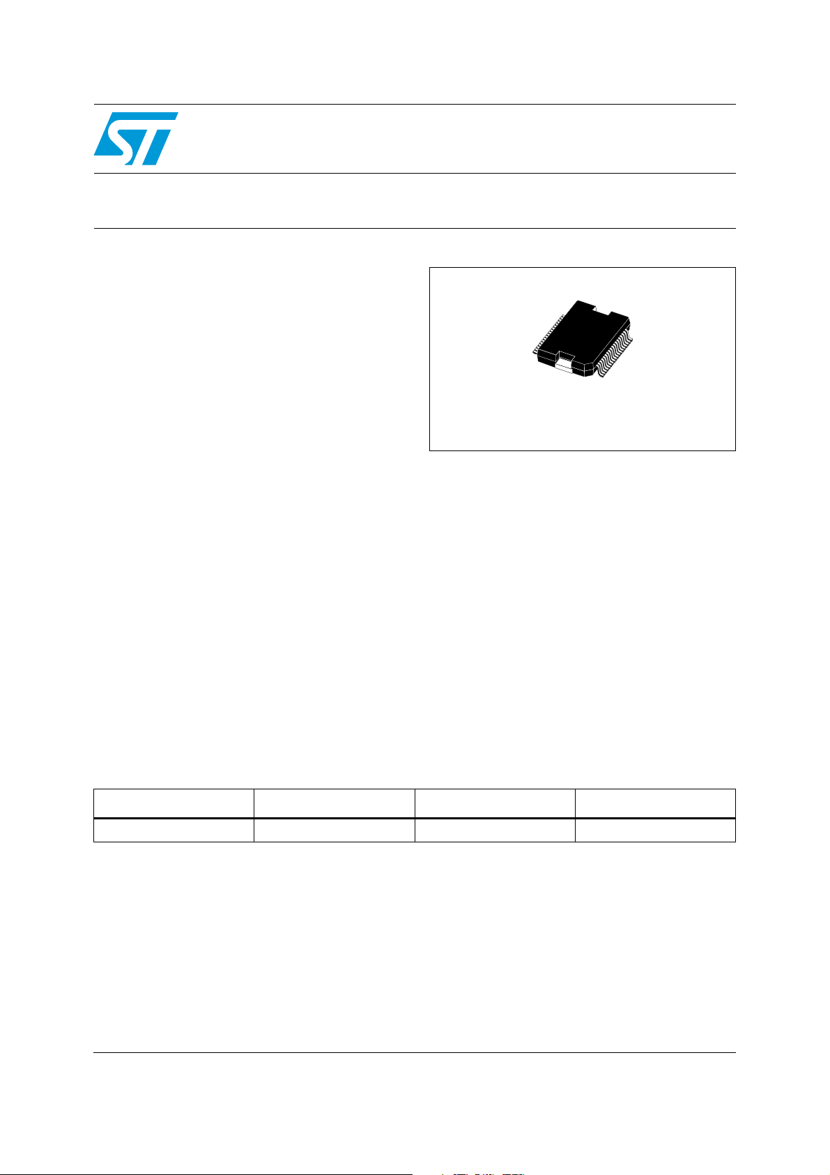
L9758
Multiple supply for engine control
PowerSO-36
■ Battery voltage thresholding - IGN
■ Logic level thresholding - PSU_EN
Description
The L9758 is a multiple output voltage regulator
utilizing linear, switchmode (buck and boost) and
tracking regulators to support high end
automotive microcontrollers used in powertrain
applications.
The L9758 provides two standby power regulators
as well as controllable LDO regulators.
The L9758 has power on reset functionality and
controlled slew rate of the V
V
.
CORE
DD5
, V
DDL
and
Order code Temperature range Package Packing
L9758 -40 °C to +125 °C PowerSO-36 Tube
November 2010 Doc ID 14273 Rev 3 1/29
www.st.com
1
Page 2

Contents L9758
Contents
1 Pins configuration . . . . . . . . . . . . . . . . . . . . . . . . . . . . . . . . . . . . . . . . . . . 6
2 Functional block diagram . . . . . . . . . . . . . . . . . . . . . . . . . . . . . . . . . . . . . 9
3 Operating conditions . . . . . . . . . . . . . . . . . . . . . . . . . . . . . . . . . . . . . . . 10
3.1 Absolute maximum ratings . . . . . . . . . . . . . . . . . . . . . . . . . . . . . . . . . . . . 10
3.2 Operating ranges . . . . . . . . . . . . . . . . . . . . . . . . . . . . . . . . . . . . . . . . . . . 11
3.3 Thermal data . . . . . . . . . . . . . . . . . . . . . . . . . . . . . . . . . . . . . . . . . . . . . . 11
4 Electrical characteristics . . . . . . . . . . . . . . . . . . . . . . . . . . . . . . . . . . . . 12
4.1 General DC characteristics . . . . . . . . . . . . . . . . . . . . . . . . . . . . . . . . . . . 12
4.2 BUCK pre-regulator . . . . . . . . . . . . . . . . . . . . . . . . . . . . . . . . . . . . . . . . . 13
4.3 Boost pre-regulator . . . . . . . . . . . . . . . . . . . . . . . . . . . . . . . . . . . . . . . . . . 14
4.4 VDD5 linear regulator . . . . . . . . . . . . . . . . . . . . . . . . . . . . . . . . . . . . . . . . 15
4.5 VDDL linear regulator . . . . . . . . . . . . . . . . . . . . . . . . . . . . . . . . . . . . . . . . 15
4.6 VCORE linear regulator . . . . . . . . . . . . . . . . . . . . . . . . . . . . . . . . . . . . . . 16
4.7 VKAM linear regulator . . . . . . . . . . . . . . . . . . . . . . . . . . . . . . . . . . . . . . . 17
4.8 VSTBY linear regulator . . . . . . . . . . . . . . . . . . . . . . . . . . . . . . . . . . . . . . . 17
4.9 VSA, VSB, VSC, VSD tracking linear regulator . . . . . . . . . . . . . . . . . . . . 18
4.10 RST5 and RSTL reset signals . . . . . . . . . . . . . . . . . . . . . . . . . . . . . . . . . 18
4.11 IGN and PSU_EN inputs . . . . . . . . . . . . . . . . . . . . . . . . . . . . . . . . . . . . . 19
4.12 STBY_OK signal . . . . . . . . . . . . . . . . . . . . . . . . . . . . . . . . . . . . . . . . . . . 20
5 Functional description . . . . . . . . . . . . . . . . . . . . . . . . . . . . . . . . . . . . . . 21
5.1 General function . . . . . . . . . . . . . . . . . . . . . . . . . . . . . . . . . . . . . . . . . . . . 21
5.2 Switching pre-regulator . . . . . . . . . . . . . . . . . . . . . . . . . . . . . . . . . . . . . . 21
5.3 VDD5, VDDL and VCORE linear regulators . . . . . . . . . . . . . . . . . . . . . . . 21
5.4 Tracking regulators . . . . . . . . . . . . . . . . . . . . . . . . . . . . . . . . . . . . . . . . . . 22
5.5 VKAM and VSTBY linear regulators . . . . . . . . . . . . . . . . . . . . . . . . . . . . . 22
5.6 RESET monitors . . . . . . . . . . . . . . . . . . . . . . . . . . . . . . . . . . . . . . . . . . . . 23
5.7 Thermal protection . . . . . . . . . . . . . . . . . . . . . . . . . . . . . . . . . . . . . . . . . . 23
5.8 Reference current . . . . . . . . . . . . . . . . . . . . . . . . . . . . . . . . . . . . . . . . . . . 23
2/29 Doc ID 14273 Rev 3
Page 3

L9758 Contents
6 Operating modes . . . . . . . . . . . . . . . . . . . . . . . . . . . . . . . . . . . . . . . . . . . 24
6.1 Standby mode . . . . . . . . . . . . . . . . . . . . . . . . . . . . . . . . . . . . . . . . . . . . . 24
6.2 Run mode . . . . . . . . . . . . . . . . . . . . . . . . . . . . . . . . . . . . . . . . . . . . . . . . . 24
6.2.1 Entry into run mode . . . . . . . . . . . . . . . . . . . . . . . . . . . . . . . . . . . . . . . . 24
6.3 Power down . . . . . . . . . . . . . . . . . . . . . . . . . . . . . . . . . . . . . . . . . . . . . . . 25
6.4 Low voltage operation . . . . . . . . . . . . . . . . . . . . . . . . . . . . . . . . . . . . . . . 25
6.5 High voltage operation . . . . . . . . . . . . . . . . . . . . . . . . . . . . . . . . . . . . . . . 26
7 Package information . . . . . . . . . . . . . . . . . . . . . . . . . . . . . . . . . . . . . . . . 27
8 Revision history . . . . . . . . . . . . . . . . . . . . . . . . . . . . . . . . . . . . . . . . . . . 28
Doc ID 14273 Rev 3 3/29
Page 4

List of tables L9758
List of tables
Table 1. Device summary . . . . . . . . . . . . . . . . . . . . . . . . . . . . . . . . . . . . . . . . . . . . . . . . . . . . . . . . . . 1
Table 2. Pins description . . . . . . . . . . . . . . . . . . . . . . . . . . . . . . . . . . . . . . . . . . . . . . . . . . . . . . . . . . 6
Table 3. Control pins description . . . . . . . . . . . . . . . . . . . . . . . . . . . . . . . . . . . . . . . . . . . . . . . . . . . . 7
Table 4. Absolute maximum ratings . . . . . . . . . . . . . . . . . . . . . . . . . . . . . . . . . . . . . . . . . . . . . . . . . 10
Table 5. Operating ranges . . . . . . . . . . . . . . . . . . . . . . . . . . . . . . . . . . . . . . . . . . . . . . . . . . . . . . . . 11
Table 6. Thermal data. . . . . . . . . . . . . . . . . . . . . . . . . . . . . . . . . . . . . . . . . . . . . . . . . . . . . . . . . . . . 11
Table 7. General DC characteristics . . . . . . . . . . . . . . . . . . . . . . . . . . . . . . . . . . . . . . . . . . . . . . . . . 12
Table 8. BUCK pre-regulator . . . . . . . . . . . . . . . . . . . . . . . . . . . . . . . . . . . . . . . . . . . . . . . . . . . . . . 13
Table 9. Boost pre-regulator . . . . . . . . . . . . . . . . . . . . . . . . . . . . . . . . . . . . . . . . . . . . . . . . . . . . . . . 14
Table 10. VDD5 linear regulator . . . . . . . . . . . . . . . . . . . . . . . . . . . . . . . . . . . . . . . . . . . . . . . . . . . . . 15
Table 11. VDDL linear regulator . . . . . . . . . . . . . . . . . . . . . . . . . . . . . . . . . . . . . . . . . . . . . . . . . . . . . 15
Table 12. VCORE linear regulator . . . . . . . . . . . . . . . . . . . . . . . . . . . . . . . . . . . . . . . . . . . . . . . . . . . 16
Table 13. VKAM linear regulator. . . . . . . . . . . . . . . . . . . . . . . . . . . . . . . . . . . . . . . . . . . . . . . . . . . . . 17
Table 14. VSTBY linear regulator . . . . . . . . . . . . . . . . . . . . . . . . . . . . . . . . . . . . . . . . . . . . . . . . . . . . 17
Table 15. VSA, VSB, VSC, VSD tracking linear regulator . . . . . . . . . . . . . . . . . . . . . . . . . . . . . . . . . 18
Table 16. RST5 reset signals . . . . . . . . . . . . . . . . . . . . . . . . . . . . . . . . . . . . . . . . . . . . . . . . . . . . . . . 18
Table 17. RSTL reset signals . . . . . . . . . . . . . . . . . . . . . . . . . . . . . . . . . . . . . . . . . . . . . . . . . . . . . . . 19
Table 18. IGN and PSU_EN inputs . . . . . . . . . . . . . . . . . . . . . . . . . . . . . . . . . . . . . . . . . . . . . . . . . . 19
Table 19. STBY_OK signal . . . . . . . . . . . . . . . . . . . . . . . . . . . . . . . . . . . . . . . . . . . . . . . . . . . . . . . . . 20
Table 20. Document revision history . . . . . . . . . . . . . . . . . . . . . . . . . . . . . . . . . . . . . . . . . . . . . . . . . 28
4/29 Doc ID 14273 Rev 3
Page 5

L9758 List of figures
List of figures
Figure 1. Pins connection (top view) . . . . . . . . . . . . . . . . . . . . . . . . . . . . . . . . . . . . . . . . . . . . . . . . . . 6
Figure 2. Functional block diagram . . . . . . . . . . . . . . . . . . . . . . . . . . . . . . . . . . . . . . . . . . . . . . . . . . . 9
Figure 3. Current reference generator . . . . . . . . . . . . . . . . . . . . . . . . . . . . . . . . . . . . . . . . . . . . . . . . 23
Figure 4. Power up/down sequence . . . . . . . . . . . . . . . . . . . . . . . . . . . . . . . . . . . . . . . . . . . . . . . . . 25
Figure 5. PowerSO-36 mechanical data and package dimensions . . . . . . . . . . . . . . . . . . . . . . . . . . 27
Doc ID 14273 Rev 3 5/29
Page 6
Pins configuration L9758
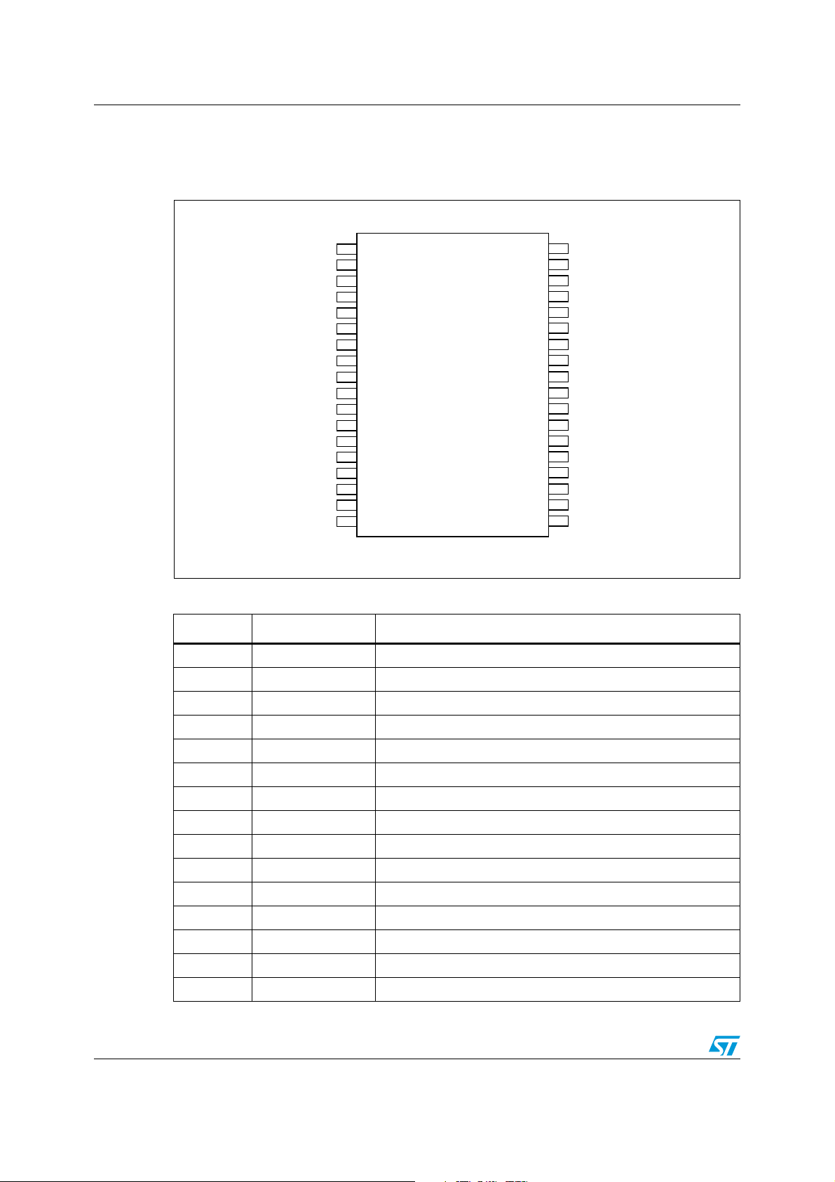
1 Pins configuration
Figure 1. Pins connection (top view)
GND
VBAT
VBAT_SW
BOOST
RES_S
GND_S
VBAT_S
IGN
IGN_ON
PSU_EN
VSD
VSC
VSB
VSA
TRACK_REF
REF_SEL
VS_DIS
REXT
Table 2. Pins description
1
2
3
4
5
6
7
8
9
10
11
12
13
14
15
16
17
18
36
35
34
33
32
31
30
29
28
27
26
25
24
23
22
21
20
19
Pin # Name Description
SW
FDBK
VB
VDD5
VDDL_DRV
VDDL_FDBK
VCORE_FDBK
VCORE_DRV
VPROG3
CORE_DIS
VPROG1
VPROG2
VKAM
VSTBY
STBY_OK
RST5
RSTL
RST_TIM
1 GND Power ground
2 VBAT Battery power source
3 VBAT_SW Switched battery power source
4 BOOST External boost transistor predriver output
5 RES_S Boost (+) current comparator input
6 GND_S Boost (-) current comparator input
7 VBAT_S Battery feedback for boost controller
8 IGN Ignition switch
9 IGN_ON Ignition state
10 PSU_EN Power supply enable
11 VSD Tracking regulator D
12 VSC Tracking regulator C
13 VSB Tracking regulator B
14 VSA Tracking regulator A
15 TRACK_REF Tracking A voltage reference
6/29 Doc ID 14273 Rev 3
Page 7
L9758 Pins configuration
Table 2. Pins description (continued)
Pin # Name Description
16 REF_SEL Tracking A voltage reference selection
17 VS_DIS Sensor supply disable
18 REXT External current reference resistance
19 RST_TIM Reset timer adjustment
20 RSTL VDDL regulator reset output
21 RST5 VDD5 regulator reset output
22 STBY_OK Standby regulator monitor
23 VSTBY Standby regulator output
24 VKAM Standby memory regulator output
25 VPROG2 Standby regulator voltage selection (VSTBY)
26 VPROG1 Standby memory regulator voltage selection (VKAM)
27 CORE_DIS VDDL and VCORE disable
28 VPROG3 VDDL voltage selection
29 VCORE_DRV VCORE external pass transistor predriver output
30 VCORE_FDBK VCORE feedback
31 VDDL_FDBK VDDL feedback
32 VDDL_DRV VDDL external pass transistor predriver output
33 VDD5 VDD5 linear regulator output
34 VB Switching preregulator output
35 FDBK Switching voltage feedback
36 SW Buck regulator switch output
Table 3. Control pins description
Pin name
Logic
level
Description
Low Enter in Stand-by Mode if also PSU_EN is low
IGN
High Enter in Run Mode
Low IGN is high
IGN_ON
High IGN is low
Low Enter in Stand-by Mode if also IGN is low
PSU_EN
High Enter in Run Mode
Low Enable VSB, VSC, VSD tracking regulators
VS_DIS
High Disable VSB, VSC, VSD tracking regulators
Low Voltage reference for VSA tracking regulator is VDD5
Ref_Sel
High
Voltage reference for VSA tracking regulator is
VTRACK_REF
Type of
I/O
Pull
down
Open
drain
Pull
down
Pull
down
Pull
down
Doc ID 14273 Rev 3 7/29
Page 8
Pins configuration L9758
Table 3. Control pins description (continued)
Pin name
RSTL
RST5
VPROG1
VPROG2
VPROG3
CORE_DIS
STBY_OK
Logic
level
Low VDDL output regulator out of range (under voltage)
High VDDL output regulator fully operational
Low VDD5 output regulator out of range (under voltage)
High VDD5 output regulator fully operational
Low VKAM regulator output programmed to 1V
High VKAM regulator output programmed to 1.5V
Low VSTBY regulator output programmed to 2.6V
High VSTBY regulator output programmed to 3.3V
Low VDLL regulator output programmed to 2.6V
High VDLL regulator output programmed to 3.3V
Low Enable VDLL and VCORE linear regulators
High Disable VDLL and VCORE linear regulators
Low VSTBY output regulator out of range (under voltage)
High VSTBY output regulator fully operational
Description
Type of
I/O
Open
collector
Open
collector
Pull up
Pull up
Pull up
Pull
down
Open
drain
8/29 Doc ID 14273 Rev 3
Page 9
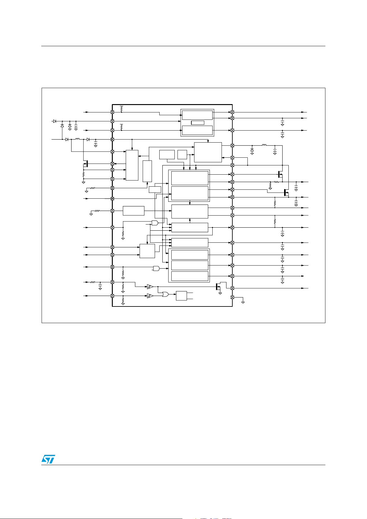
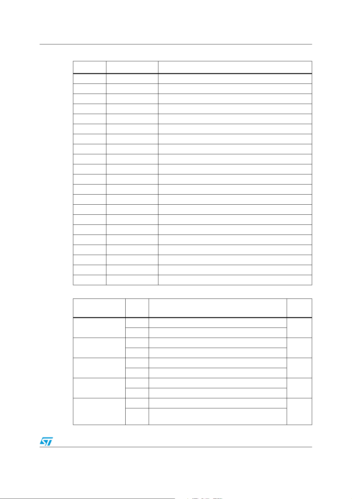
L9758 Functional block diagram
2 Functional block diagram
Figure 2. Functional block diagram
VBAT
STBY
VBAT
RUN
22 µH
10 µF
0.1
TRACK_REF
VPROG2
VBAT
VPROG1
VBAT_SW
300µF
VBAT_S
BOOST
RES_S
GND_S
REXT
10K
VPROG3
RST_TIM
Rtim
CORE_DIS
REF_SEL
VS_DIS
51K
IGN
100 nF
PSU_EN
Boost
Oscillator
/ Divider
EN_REG
Control
Analog
MUX
EN_REG
Charge
Pump
(5 MHz)
SMPS Osc.
SOFT
START
STBY Vreg
2.6V/3.3V, 10mA
Bandgap
VKAM Vreg
1V/1.5V, 10mA
1.5V, 1.0A
5V, 1.0A
50mA
50mA
50mA
50mA
Switchmode
VCORE
VDDL
VDD5
VSA
VSB
VSC
VSD
EN_REG
SOFT START
Band
Gap
Ref.
Linear Voltage Controller
Linear Voltage Controller
2.5V / 3.5V, 1.0A
RESET Logic
VDDL Undervoltage
VDD5 Undervoltage
Power On Reset
Linear Voltage Regulator
Tracking Regulator
Tracking Regulator
Tracking Regulator
Tracking Regulator
Power
Up/Dn
Buck
Power
Supply
Open Drain
STBY_OK
VSTBY
VKAM
SW
FDBK
VB
VCORE_DRV
VCORE_FDBK
VDDL_DRV
VDDL_FDBK
RSTL
RST5
VDD5
VSA
VSB
VSC
VSD
IGN_ON
GND
22 µH
22 µF
2.4K
5.1K
1 µF
1 µF
VCORE_FDBK
22 uF
VDDL
22 uF
10µF
2.2µF
2.2µF
2.2µF
2.2µF
Doc ID 14273 Rev 3 9/29
Page 10

Operating conditions L9758
3 Operating conditions
3.1 Absolute maximum ratings
This part may be irreparably damaged if taken outside the specified absolute maximum ratings.
Operation above the absolute maximum ratings may also cause a decrease in reliability.
Table 4. Absolute maximum ratings
Symbol Parameter Value Unit
VBAT,V
, V
V
V
I-digital
V
I-analog
V
V
V
O-digital
V
V
V
CORE_DRV
V
DDL_DRV
I
SMPS
T
V
BAT_SW
BAT_S
IGN
V
B
FDBK
SW
OR
VSx
T
op
stg
T
j
ESD
Battery supply voltage -0.3 to 40 V
Ignition input voltage (with at least 10K external resistance) -2.0 to 40 V
Digital input voltages (PSU_EN, VS_EN, VPROG1,
VPROG2, VPROG3, VDDL/VCORE_EN, REF_SEL)
Analog input voltages (REXT, TRACK_REF, RST_TIM
VDDL_FDBK, VCORE_FDBK)
-0.3 to 7 V
-0.3 to 7 V
Linear regulator supply (VB) -0.3 to 40 V
Switching feedback (FDBK) -0.3 to 40 V
Buck regulator switch output (SW) -2 to 40 V
Digital output voltages (IGN_ON, RSTL, RST5, BOOST,
STBY_OK)
-0.3 to 7 V
Regulator output voltages (VDD5, VSTBY, VKAM) -0.3 to 7 V
Regulator output voltages (VSA, VSB, VSC, VSD) -3 to 40 V
,
External regulator predriver output (VCORE_DRV,
VDDL_DRV)
-0.3 to 15 V
Switching preregulator current 0 to 4.2 A
Operating temperature -40 to 125 °C
Storage temperature -50 to 150 °C
Max junction temperature 150 °C
Max ESD (human body model) ±2 KV
Warning: Exceeding these values might destroy this part. This part is
not guaranteed to function properly at these ratings.
The CMOS inputs and outputs should never go above 5V +
0.3V or below GND - 0.3V without protection (series
resistance). If this occurs, the device might be destroyed by
latch-up and/or the output levels might not be controlled by
the inputs. Unused inputs must be connected to GND and
unused outputs should be left open and programmed to a low
state. Unused I/O pins should be programmed as outputs, left
open, and programmed to a low state.
10/29 Doc ID 14273 Rev 3
Page 11

L9758 Operating conditions
3.2 Operating ranges
Full specification parameters cannot be guaranteed outside the operating ranges. Once the
condition is returned to within the specified operating ranges, the part will recover with no
damage or degradation.
Table 5. Operating ranges
Symbol Parameter Value Unit
V
BAT
, V
V
BAT_S
V
V
I-digita
V
I-analog
I
AVE
T
IGN
T
BAT_SW
l
op
j
,
Battery supply voltage
Ignition input voltage (with at least 10K external
resistance)
Digital input voltages (PSU_EN,VS_EN,VPROG1,
VPROG2, VPROG3, VDDL/VCORE_EN, REF_SEL)
Analog input voltages (REXT, TRACK_REF, RST_TIM
VDDL_FDBK, VCORE_FDBK)
Switching preregulator average current 0 to 2.5 A
Operating temperature -40 to 125 °C
Junction temperature -40 to 150 °C
3.3 Thermal data
Table 6. Thermal data
Symbol Parameter Value Unit
R
th(j-case)
Thermal resistance junction-to-case 2 °C/W
4 to 26.5
4 to 40
(t < 400ms)
4 to 26.5 V
-0.3 to 5.3 V
-0.3 to 5.3 V
V
Doc ID 14273 Rev 3 11/29
Page 12

Electrical characteristics L9758
4 Electrical characteristics
All voltage values are, if not otherwise stated, relative to ground.Current flow into a pin is
positive. If not otherwise stated, all rise times are between 10% and 90%, fall times between
90% and 10% and delay times at 50% of the relevant steps.
4.1 General DC characteristics
T
= -40 °C to 125 °C, V
amb
Table 7. General DC characteristics
Symbol Parameter Test condition Min. Typ. Max. Unit
BAT
= V
BAT_SW
= 5.5 to 26.5 V, unless otherwise specified.
I
BAT_SW_SB
I
Q_OFF
V
LV I_ LO W
V
LV I_ HI G H
V
LV I_ H YS
V
ST
V
REXT
V
TH_VSEN
V
VDDL/VCORE_EN
V
PROG1_LOW
V
PROG2_LOW
V
PROG3_LOW
Quiescent current at pin
BAT_SW
Supply current in OFF
state
Low voltage inhibit Low
threshold
Low voltage inhibit High
threshold
Low voltage inhibit
hysteresis
V
= 0 V;
BAT
BAT_SW
= 12 V
+ I
VBAT
--120µA
V
I
VBAT_SW
-3.5-3.9V
-4.0-4.5V
-0.3-1V
Linear Start-up voltage - 3.8 - 4.8 V
Rext Voltage - 1.18 - 1.24 V
VS_EN input threshold - 0.8 - 2 V
VDDL/VCORE_EN
input threshold
PROG1 input Low
Voltage
PROG2 input Low
Voltage
PROG3 input Low
Voltage
-0.8-2V
---0.8V
---0.8V
---0.8V
V
DDL_ENUP
Vddl Power-up enable - 1 - 2 V
12/29 Doc ID 14273 Rev 3
Page 13

L9758 Electrical characteristics
4.2 BUCK pre-regulator
T
= -40 °C to 125 °C, V
amb
Table 8. BUCK pre-regulator
Symbol Parameter Test condition Min. Typ. Max. Unit
F
SW
R
dsON
I
ST_MAX
Operating frequency
High side switch ON
resistance
Average current during
start-up
= V
BAT
R
V
V
V
BAT_SW
= 10.0 kOhm ±1%
ext
= 13.5 V
BAT_SW
= 6.0V - - 0.25 Ω
BAT_SW
= 3.0V 0.3 - 0.7 A
B
= 5.5 to 26.5 V; unless otherwise specified.
300 - 450 kHz
V
BREG
Vb100
Output voltage
100% Duty Cycle operation
threshold
7.0V < V
0.25A < I
BAT_SW
<2.0A
VBAT
< 18V
5.5 - 6.1 V
6.2 - 7.8 V
Voltage sensed at VBAT_SW pin
Vb100h
ΔVpre Load regulation ΔI
Vrpre Voltage ripple, p-p
100% Duty Cycle operation
threshold hysteresis
= 0.1A –2A V
VB
BAT_SW
L = 22µH, C = 22µF X7R
BAT_SW
= 13.5V
V
0.05 - 0.8 V
= 13.5V - - 400 mV
--300mV
Ts Start time L = 22µH, C = 22µF X7R - - 1.4 ms
DCmin Minimum duty cycle - 10 - 18 %
EFF Efficiency
L
Rs
C
ESR
Output Inductance -
Output capacitance -
Ov Power-up overvoltage
Tr _s w
Tf_sw
SW rising and falling time
V
V
V
0.25A < I
7.0V < V
I
VBAT
= 13.5 V IVB = 0.5A
BAT_SW
= 13.5V IVB = 2A
BAT_SW
< 26.5V
BAT_SW
VBAT
BAT_SW
<2.0A (20%, 80%)
<2.0A
< 18V
70
70
-- %
15 22 30
75
10
0
-
100
160µFmΩ
15 - 200 mV
10 - 150 µs
µH
mΩ
Doc ID 14273 Rev 3 13/29
Page 14

Electrical characteristics L9758
4.3 Boost pre-regulator
T
= -40 °C to 125 °C, V
amb
Table 9. Boost pre-regulator
Symbol Parameter Test condition Min. Typ. Max. Unit
FSW Operating frequency
V
B_REG
Output voltage 4.0 V < V
BoostONth Boost enable threshold
BoostOFFth
V
BOOST_HY
ΔV
BOOST
V
R_VBOOST
V
OLB
V
OHB
Boost disable threshold 7.0 - 8.3 V
Boost operation threshold
hysteresis
Load regulation ΔIVB = 0.1 A–2 A V
Voltage ripple, p-p
Boost predriver low level
voltage
Boost predriver low level
voltage
= V
BAT
R
V
BAT_SW
= 10.0 kOhm ±1%
ext
= 13.5 V
BAT_SW
= 5.5 to 26.5 V, unless otherwise specified.
300 - 450 kHz
< 7 V, 0.25 A < IVB < 2.0 A 8.5 - 10 V
BAT_S
7.0 - 8.3 V
Voltage sensed at VBAT_S pin
Voltage sensed at VBAT_S pin 0.05 - 0.9 V
= 4 V - - 600 mV
BAT_S
L = 22 µH, C = 300 µF X7RX7R
= 4 V
V
BAT_S
= 1 mA - - 0.2 V
I
sink
I
= 200 µA 4.8 - - V
source
- - 600 mV
T
T
ESR
R
SENSE
RB
FB
L
Rs
C
Boost predriver rise time Cl = 1 nF 50 - 180 ns
Boost predriver fall time Cl = 1 nF 20 - 100 ns
Output inductance - 15 22
Output capacitance -
10010300 900
3075µH
mΩ
200µFmΩ
Sensing resistor - 40 50 - mΩ
14/29 Doc ID 14273 Rev 3
Page 15

L9758 Electrical characteristics
4.4 VDD5 linear regulator
T
= -40 °C to 125 °C, V
amb
Table 10. VDD5 linear regulator
Symbol Parameter Test condition Min. Typ. Max. Unit
BAT
= V
BAT_SW
= 5.5 to 26.5 V, unless otherwise specified.
5 mA < I
5 mA < I
V
Output voltage
DD5
V
BAT_SW
5 mA < I
I
DD5_LIM
C
DD5
ESR
R
RDD5
V
DD5_MAX
ΔV
DD5
I
DD5
V
lineR Line regulation 6.0 V < VB < 7 V -25 - +25 mV
DD5
loadR Load regulation 5 mA < I
V
DD5
V
DD5-Vddl
Current limit V
Output capacitor
= 4.75 V 1200 - 2500 mA
DD5
Ceramic or Tantalum
C = 4.7µF
Ripple rejection F = 375 kHz 26 - - dB
Maximum overshoot
Output voltage slew rate
/Δt
at power-up
ΔVB/Δt < 70 V/ms
V
BAT_SW
5 mA < I
Load current - 5 - 1000 mA
Start up V
DD5-Vddl
4.5 VDDL linear regulator
-
-
5.1
4.0
100
160µFmΩ
< 1 A V
DD5
< 800 mA
DD5
BAT_SW
=> 5.7 V
4.9
= 5.5 V
DD5
< 1 A V
BAT_SW
≥ 4 V
3.3
4.7
0
= 4V ⇒ 8 V
< 1 A V
DD5
< 1 A -25 - +25 mV
DD5
= 13.5 V 10 - 20 V/ms
BAT_SW
--5.5V
during start up 0.5 - 3.1 mV
V
T
= -40 °C to 125 °C, V
amb
Table 11. VDDL linear regulator
BAT
= V
BAT_SW
= 5.5 to 26.5 V, unless otherwise specified.
Symbol Parameter Test condition Min. Typ. Max. Unit
V
C
ESR
RR
DDL
DDL
DDL
5 mA < I
4.0 V < V
< 1 A, V
DDL
BAT_SW
< 18 V
Output voltage
5 mA <I
4.0 V < V
< 1 A, V
DDL
BAT_SW
< 18 V
Output capacitor Ceramic or Tantalum
Ripple rejection F= 375 kHz 26 - - dB
PROG3
PROG3
= Open
= Low
3.23
2.55
4.7
0
3.37
-
2.65
-
Doc ID 14273 Rev 3 15/29
V
100
160µFmΩ
Page 16

Electrical characteristics L9758
Table 11. VDDL linear regulator (continued)
Symbol Parameter Test condition Min. Typ. Max. Unit
V
DDL_MAX
Maximum
overshoot
5 mA <I
4.0 V < V
ΔVB/Δt < 70 V/ms
5 mA < I
4.0 V < V
< 1 A, V
DDL
BAT_SW
DDL
BAT_SW
< 18 V
< 1 A, V
< 18 V
PROG3
PROG3
= Open
= Low
3.75
--
ΔVB/Δt < 70 V/ms
ΔV
/Δt
DDL
I
DDL
V
lineR Line regulation 5.5 V < V
DDL
loadR Load regulation 5 mA < I
V
DDL
Output voltage slew
rate at power-up
5 mA <I
DDL
< 1 A V
=13.5 V 5 - 25 V/ms
BAT_SW
Load current 5 - 1000 mA
< 7 V -8 - +8 mV
BAT_SW
< 1 A -8 - +8 mV
DDL
4.6 VCORE linear regulator
T
= -40 °C to 125 °C, V
amb
Table 12. VCORE linear regulator
Symbol Parameter Test condition Min. Typ. Max. Unit
V
CORE
CddL
ESR
Output voltage 5mA < I
Output capacitor Ceramic or Tantalum
BAT
= V
BAT_SW
< 1A 4.0V < V
CORE
= 5.5 to 26.5 V, unless otherwise specified.
< 18V 1.47 - 1.53 V
BAT_SW
4.70
0
-
V
3.6
100
160µFmΩ
RRddL Ripple rejection F= 375 kHz 26 - - dB
V
CORE_M
ΔV
V
CORE_PROG
V
V
V
/Δt
CORE
I
CORE
CORE_FBK
lineR Line regulation 5.5 V < V
CORE
loadR Load regulation 5 mA < I
CORE
Maximum
overshoot
Output voltage slew
rate at power-up
Load current - 5 - 1000 mA
Range of
programmability
Feedback voltage - 0.98 - 1.02 V
5 mA < I
4.0 V < V
5 mA < I
CORE
BAT_SW
CORE
< 1 A
< 18 V
< 1 A V
--1.7V
=13.5 V 5 - 25 V/ms
BAT_SW
Using external resistor divider 1.05 1.5 2.8 V
< 7 V -25 - +25 mV
BAT_SW
< 1 A -25 - +25 mV
CORE
16/29 Doc ID 14273 Rev 3
Page 17

L9758 Electrical characteristics
4.7 VKAM linear regulator
T
= -40 °C to 125 °C, V
amb
Table 13. VKAM linear regulator
Symbol Parameter Test condition Min. Typ. Max. Unit
BAT
= V
BAT_SW
= 5.5 to 26.5 V, unless otherwise specified.
C
RR
V
KAM
VKAM
ESR
VKAM
Output voltage
Output capacitor Ceramic
Ripple rejection F=375 kHz 26 - dB
Maximum overshoot
V
KAM_M
(absolute value
relative to GND)
Iddkamsh Current limit V
I
KAM
V
lineR Line regulation 6 V < V
KAM
loadR Load regulation 0.1 mA < I
V
KAM
Load current - 0.1 - 10 mA
0.1mA < I
4.0V < V
0.1mA < I
4.0V < V
VKAM
BAT
VKAM
BAT
< 10mA, V
< 18V
< 10mA, V
< 18V
PROG1
PROG1
= Low
=Open
0.9
1.37
0.1
0
0.1 mA < I
4V < V
BAT
0.1 mA < I
4V < V
BAT
= 0.5 V 11 - 50 mA
KAM
BAT
< 10 mA, V
VKAM
< 18 V
< 10 mA, V
VKAM
< 18 V
< 18 V -25 - +25 mV
< 10 mA -25 - +25 mV
KAM
PROG1
PROG1
= Low
=Open
--
-
-
1.1
1.65
4.720µF
1.2
1.7
4.8 VSTBY linear regulator
T
= -40 °C to 125 °C, V
amb
Table 14. VSTBY linear regulator
Symbol Parameter Test condition Min. Typ. Max. Unit
V
C
RR
STBY
STBY
ESR
STBY
Output voltage
Output capacitor Ceramic
Ripple rejection F = 350 kHz 26 - - dB
Maximum overshoot
V
STBY_M
(absolute value
relative to GND)
I
sh Current limit V
STBY
I
STBY
lineR Line regulation 6 V < V
V
STBY
loadR Load regulation 0.1 mA < I
V
STBY
Load current - 0.1 - 10 mA
= V
BAT
0.1 mA < I
4 V < V
0.1 mA < I
4 V < V
0.1 mA < I
4 V < V
0.1 mA < I
4 V < V
STBY
BAT_SW
STBY
< 18 V
BAT
STBY
< 18 V
BAT
STBY
< 18 V
BAT
STBY
< 18 V
BAT
= 0.5 V 11 - 50 mA
<18 V -25 - +25 mV
BAT
STBY
= 5.5 to 26.5 V, unless otherwise specified.
< 10 mA, V
< 10 mA, V
< 10 mA, V
< 10 mA, V
< 10 mA -25 - +25 mV
PROG2
PROG2
PROG2
PROG2
= Low
= Open
= Low
= Open
2.47
3.13
0.1
0
-
-
--
2.73
3.47
10
20µFmΩ
3.05
3.75
V
mΩ
V
V
V
Doc ID 14273 Rev 3 17/29
Page 18

Electrical characteristics L9758
4.9 VSA, VSB, VSC, VSD tracking linear regulator
Table 15. VSA, VSB, VSC, VSD tracking linear regulator
T
= -40 °C to 125 °C, V
amb
BAT
= V
BAT_SW
= 5.5 to 26.5 V, unless otherwise specified.
Symbol Parameter Test condition Min. Typ. Max. Unit
ΔV
TRK
sh Current limit V
I
TRK
C
TRK
ESR
Ctckmin
ESRmin
RR
TRK
Output voltage
tracking accuracy
Output load capacitor Ceramic or Tantalum
Minimum output
capacitor for stability
Ripple rejection F= 375 kHz 26 - - dB
Vdrop Dropout voltage I
T
T
I
TSD
HYST
TRK
Thermal shutdown Vtck = 4.75V (current limitation) 165 - 185 °C
Thermal hysteresis Vtck = 4.75V (current limitation) 5 - 15 °C
Load current - 1 - 50 mA
1 mA < It1 < 50 mA, 6 V < V
1 mA < It1 < 5 0mA, 4 V < V
= 4.75 V 51 - 100 mA
tck
BAT_SW
BAT_SW
< 18 V
< 6 V
-7
-50
1
0
Ceramic or Tantalum
= 50mA - - 300 mV
load
1
0
10
50
16
-
-
4.10 RST5 and RSTL reset signals
mV
µF
3
mΩ
µF
3
Ω
T
= -40 °C to 125 °C, V
amb
Table 16. RST5 reset signals
BAT
= V
BAT_SW
= 5.5 to 26.5 V, unless otherwise specified.
Symbol Parameter Test condition Min. Typ. Max. Unit
I
RST5_H
V
RST5_L
V
FTH_RST5
V
RTH_RST5
V
HY_RST5
t
ACT_RST5
t
DEL_RST5
t
ERR_RST5
Reset “high” leakage
current
Reset “low” output
voltage
Reset threshold
decreasing
Reset threshold
increasing
Reset threshold
hysteresis
Reset activation out
of tolerance duration
= 5.15 V -3.0 - - µA
V
RST5
= 4.5 V Ire = 5 mA
V
DD5
= 1.0 V Ire = 1 mA
V
DD5
ΔV
DD5/Δt
ΔV
DD5/Δt
-50--mV
- 15 - 25 µs
Reset delay 4.7 kΩ < R
Reset delay accuracy R
±1% -15 - +15 %
ext
V
V
0.07
0.4
0.4
DD5
0.2
DD5
--
< 0 4.5 -
> 0 4.5 -
< 47 kΩ 1-10ms
ext
V
–
V
–
V
18/29 Doc ID 14273 Rev 3
Page 19

L9758 Electrical characteristics
Table 17. RSTL reset signals
Symbol Parameter Test condition Min. Typ. Max. Unit
I
RSTL_H
V
RSTL_L
V
FTH_RSTL
V
RTH_RSTL
V
FTH_RSTL_O
V
RTH_RSTL_O
V
HY_RSTL
t
ACT_RSTL
t
DEL_RSTL
t
ERR_RSTL
Reset “high”
leakage current
Reset “low” output
voltage
Reset threshold
decreasing
Reset threshold
increasing
Reset threshold
decreasing
Reset threshold
increasing
Reset threshold
hysteresis
Reset activation out
of tolerance duration
= 5.15 V -3.0 - - µA
V
DDL
=5.0V Ire=5mA
V
DDL
=1.0V Ire=1mA
V
DDL
ΔV
DDL
ΔV
DDL
ΔV
DDL
ΔV
DDL
-40--mV
-15-25μs
Reset delay 1nF < C
Reset delay
accuracy
R
±1% -15 - +15 %
ext
/Δt < 0, V
/Δt < 0, V
/Δt < 0, V
/Δt < 0, V
EXT
PROG3
PROG3
PROG3
PROG3
< 10nF; 4.7kΩ < R
--
=Low 2.375 -
=Low 2.375 -
=Open 3.13 -
=Open 3.13 -
< 47kΩ 1- 10 ms
ext
V
0.05
V
0.02
V
0.05
V
0.02
0.4
0.4
DDL
DDL
DDL
DDL
–
–
–
–
V
V
V
V
V
4.11 IGN and PSU_EN inputs
T
= -40 °C to 125 °C, V
amb
Table 18. IGN and PSU_EN inputs
Symbol Parameter Test condition Min. Typ. Max. Unit
V
TH_IGN
V
HYS_IGN
R
PD_IGN
V
TH_PSUEN
V
HYS_PSUEN
R
PD_PSUEN
V
OL_IGNON
R
IGN_EXT
IGN input threshold threshold @ IGN pin 2 - 3.6 V
IGN input threshold
hysteresis
IGN pull-down resistor - 300 - 1100 kΩ
PSU_EN input threshold - 0.9 -
PSU_EN input threshold
hysteresis
PSU pull-down resistor - 50 - 230 kΩ
IGN_ON “low” output
voltage
IGN external input
resistance
BAT
= V
BAT_SW
= 5.5 to 26.5 V, unless otherwise specified.
- 0.2 - 1.4 V
0.55*
V
STBY
- 0.2 - 0.8 V
Iol=1mA 0.4 V
10 50 kΩ
V
Doc ID 14273 Rev 3 19/29
Page 20

Electrical characteristics L9758
4.12 STBY_OK signal
Table 19. STBY_OK signal
T
= -40°C to 125°C, V
amb
BAT
= V
BAT_SW
= 5.5 to 26.5V, unless otherwise specified.
Symbol Parameter Conditions Min Max Units
T
h_stbyok
T
stbydly
T
stbyok
V
ol_stbyok
VstanbyOK threshold ΔV
STBY_OK filter time 15 25 µs
STBY_OK delay accuracy 10 60 µs
STBY_OK low output
voltage
/Δt <0 -8,5 -3,5 %
STBY
V
STBY
=1V I
=1mA 0.4 V
stbyok
20/29 Doc ID 14273 Rev 3
Page 21

L9758 Functional description
5 Functional description
5.1 General function
The L9758 is equipped with 9 linear voltage regulator. A buck boost switch mode power
supply as pre regulator for the 7 main regulators is used to reduce the power consumption in
the system.
Two standby regulators can be used to bias the system on off-mode. This to regulator’s are
equipped with a independent bandgap voltage reference. The current consumption of these
two linear regulators is specified with less than 120 µA in OFF state. I these standby
function is not used the current consumption on the battery can be reduced by not
connecting the VBAT. Under this condition the device enters immediately in the run mode,
the pin PSU_REN will lost his function. The quiescent current on the VBAT_SW can be
reduced to maximum 10 µA with 12 V battery voltage in off mode. The main regulators can
be activated with the IGN input. With a external resistor higher than 10 kohm in series to the
IGN pin a battery compliant signal can be used. In the function block diagram a resistor
value of 51 kohm is mention and a 100 nF capacitor for noise robustness on IGN.
5.2 Switching pre-regulator
The switching pre-regulator is a buck or a buck-boost current control mode regulator. The
optional boost operation for low battery conditions can be selected connecting external logic
level low side NCH FET and an external diode in series to the inductor.
The external parts required to complete the switching regulator are an inductor, recirculation
diode and input and output filtering capacitor. The compensation network is inside the
device.
With a constant switching frequency of 350 kHz, the pre-regulator controls the output
voltage (the voltage at the VB and FDBK pins) to the limits stated in the electrical
characteristics table varying the duty cycle. The 350 kHz are related to R
Section 5.8).
At low battery voltages, in buck configuration, the pre-regulator runs with the duty cycle up
to 100%. In buck-boost configuration normally it runs at 350 kHz but for a limited range of
input voltage it could enter in pulse skipping mode to control the output voltage.
A soft start function is implemented reducing the current limitation during the power-up
phase.
5.3 VDD5, VDDL and VCORE linear regulators
The VDD5 output is a fully integrated low drop out regulator. The V
will be implemented via an external N-channel pass MOS, with the control being internal to
the IC. If the pass MOS is not used, two low current (max 30mA) regulator are available
connecting directly VDDL_FDBK to VDDL_DRV and VCORE_FDBK to VCORE_DRV with a
resistor divider.The output of the pre-regulator is used as the source of these supplies.
DDL
= 10 kΩ (see
EXT
and V
CORE
supplies
V
is a fixed 5V nominal output, while V
DD5
and V
DDL
Doc ID 14273 Rev 3 21/29
are programmable.
CORE
Page 22

Functional description L9758
The V
voltage is selectable with the VPROG3 pin: 2.5V if connected to GND and 3.3V if
DDL
is left open (an internal pull-up is present). V
external resistor divider at the feedback pin (VCORE_FDBK).
Once programmed to a value at power-up, this value cannot change during the power cycle.
It is the intent that the system run at a single fixed value for V
the product.
All the linear regulators start with a controlled slew rate when the pre-regulated voltage
reaches V
DDL_ENUP
threshold as indicated in the electrical characteristics table. All the
linear regulator are short circuit protected with a limited current.
5.4 Tracking regulators
Four low drop-out tracking regulators (VSA, VSB, VSC and VSD) are supplied by the output
of the switching pre-regulator. They track the output voltage of the VDD5 linear regulator
with the accuracy as specified in the electrical characteristic table.
The VSA regulator also tracks an external voltage reference (TRACK_REF pin) and the
tracking voltage is selected by the REF_SEL pin.
If REF_SEL is tied High (5V) then V
tracked. There is an internal pull-down on REF_SEL.
The tracking supplies are intended to drive loads that are external to the ECU so they are
short circuit protected with the current limited. The outputs of the tracking regulators also
withstand short circuit to the battery.
TRK_REF
voltage is programmable connecting an
CORE
DDL
and V
for the life of
CORE
is tracked. If REF_SEL is left open then V
DD5
is
A short circuit to GND, continuous or intermittent on one tracking supply will not affect any
other supply, including the preregulator output voltage V
all sensor supplies shall be capable of operating with up to a 15µF load on the supply line.
This load may be present during initial startup, or be applied after the supply has been
powered up. In either case, the application of this load shall not cause the tracking
regulators to be permanently disabled.
VSB, VSC and VSD regulators can be disabled with VS_EN pin.
5.5 VKAM and VSTBY linear regulators
These two outputs are fully integrated low quiescent current low drop out regulators. The
input VBAT is used as the source of these supplies. These outputs are operational during
both standby and run mode; these are the only outputs operational during standby (V
present).
The VKAM regulator has two programmable levels: 1.0V (VPROG1 pin connected to GND)
or 1.5V (if this pin is left open, an internal pull-up is present).
The V
or 3.3V (if this pin is left open, an internal pull-up is present).
The STBY_OK pin indicates when the V
indicated in the electrical characteristic table). Once driven low it should stay low for a
minimal amount of time allowing external circuitry to latch.
regulator has two programmable levels: 2.6V (VPROG2 pin connected to GND)
STBY
is out of range (voltage below the threshold
STBY
. In addition to these requirements,
B
not
BAT
22/29 Doc ID 14273 Rev 3
Page 23

L9758 Functional description
5.6 RESET monitors
RST5 is the reset signal tied to the V
that pulls low when V
is out of range.
DD5
RSTL is the reset signal for the V
pulls low when V
is out of range. RST5 and RSTL are also driven low when STBY_OK
DDL
pin is driven low, regardless of the status of V
Reset Delay is the time duration from when the output (V
when the reset pin (RST5 or RSTL) is released. RST5 and RSTL use separate timers. This
delay is programmable via an external resistor connected to RST_TIM pin. A value of 4.7 kΩ
corresponds to 1 ms and 47 kΩ to 10 ms. All values in between are linear approximated.
The timer delay is common however the attack and release times are only dependant on the
condition of the respective supplies (V
5.7 Thermal protection
The tracking regulators incorporate thermal limit with shutdown. When the junction
temperature reaches the shutdown threshold, if there is a tracking regulator in current
limitation, it switches off and all the other regulators stay on. When the temperature
decrease the regulator restarts. The over temperature shutdown has an hysteresis to avoid
thermal pumping.
5.8 Reference current
supply. This is an open collector active low signal
DD5
supply. This is an open collector active low signal that
DDL
DD5
or V
DD5
DDL
and V
).
DDL
DD5
.
or V
) is within range to
DDL
The L9758 provides a DC voltage at the REXT pin. An external resistor to ground creates a
reference current which is mirrored internally for use in the device.
The reference current is used to supply all the analog blocks and to charge and discharge
an integrated capacitor to generate a 5 MHz clock for the switching functionality.
Figure 3. Current reference generator
Iref
Iref
+
Iref
Iref
R
R
ext
ext
+
-
+
+
V
V
ref
ref
-
-
The circuit is designed for a 10 kΩ resistor. For all affected parameters, this resistor value is
mentioned in the electrical characteristics section.
Doc ID 14273 Rev 3 23/29
Page 24

Operating modes L9758
6 Operating modes
There are two modes of operation of the power supply: standby and run mode. However
during RUN mode, there are three input voltage regions: low voltage, normal voltage and
high voltage. A brief definition and description of each of these operating regions is
described below.
6.1 Standby mode
STANDBY mode is defined by the following conditions:
● VBAT is within the required voltage range
● VBAT_SW may or may not be present
● IGN is in the OFF state
● PSU_EN is not asserted by the microprocessor
During standby mode, all functions are shutdown except the two standby supplies, VKAM
and VSTBY, and the circuitry monitoring IGN and PSU_EN. During standby mode, current
consumption is minimized. The standby functions are powered from VBAT.
There is no currents drawn from VBAT_SW or any other input except those required to
perform the standby functions. Outputs, other than IGN_ON are disabled, sourcing nor
sinking current.
6.2 Run mode
RUN mode is defined by the following conditions:
● VBAT is within the required range
● VBAT_SW is within the required range
● Either IGN is in the Run state and/or PSU_EN is in the active state
During RUN mode, all functions can be enabled. All functions listed above, with the
exception of the standby functions, are powered by VBAT_SW.
If VBAT is not present, the circuit is fully running with the exception of PSU_EN and the
standby functions (VKAM and VSTBY). In this condition the entry into the RUN MODE can
only be performed by the IGN pin and the circuit is kept running until IGN pin is in pulled low.
6.2.1 Entry into run mode
RUN mode is entered when at least one of the two signals IGN_SW or PSU_EN goes in the
active state. These two signals may be applied in any order or simultaneously.
When the IGN input is valid, the active low IGN_ON signal is asserted.
The design of VDD5, VDDL and VCORE regulators limits the slew rate of the output
voltages during the start-up as indicated in the electrical characteristic table and ensures
that V
As indicated in Figure 4, the switching regulator starts first with soft start control or reduced
current limitation. When the VB voltage reaches the VDDL_ENUP threshold all the linear
regulator start with controlled slew-rate. The slew-rate control is done controlling the slew
is always greater than V
DD5
DDL
and V
CORE
.
24/29 Doc ID 14273 Rev 3
Page 25

L9758 Operating modes
rate of the common voltage reference so the slew is different for each regulator because all
start together and reach the steady-state at the same time but with different voltage levels.
6.3 Power down
The power down sequence starts when both IGN and PSU_EN signal are low. In this phase
there is no control of the linear regulator output voltages. The falling slew-rate is defined
from load currents and load capacitors. A voltage comparator controls VDDL voltage and
ensures that the VDDL supply voltage will drop below 2V before initiating a new power-up
sequence.
Figure 4. Power up/down sequence
IGN
or
PSU_EN
Vth_Start
VB
Soft start
VDD5
Slew rate
control
VDDL
VCORE
Inductor
current
Current
limitation
RST5
RSTL
6.4 Low voltage operation
When L9758 is up and running it is fully operational with the VBAT and VBAT_SW pin
voltages down to V
LV I_ L OW
than 5.5V and are greater or equal to V
operational. If only the buck regulator is used the L9758 operates as follow:
● Switching regulator runs at 100% duty cycle
● VKAM and VSTBY regulators are fully operational
● VDDL fully operational
● VCORE fully operational
● VDD5 out of range with output voltage no less than 3.2V
● Tracking regulators out of range with output voltages no less than 3.2V
● Reset monitor RST5 and RSTL fully operational, with reset at RST5 pin in allowed
. When L9758 is up and running and the supply voltages are less
LV I_ L OW
if the boost option is used the device is fully
Doc ID 14273 Rev 3 25/29
Page 26

Operating modes L9758
6.5 High voltage operation
The L9758 is fully operational during jump start when the battery is temporarily replaced
with a higher voltage source to aid starting the engine (26.5V for 1 minute). The L9758 is
fully operational during positive battery transient such as load dump (40V maximum voltage
with durations of up to 400ms).
26/29 Doc ID 14273 Rev 3
Page 27

L9758 Package information
7 Package information
In order to meet environmental requirements, ST offers these devices in different grades of
ECOPACK
®
packages, depending on their level of environmental compliance. ECOPACK
®
specifications, grade definitions and product status are available at: www.st.com.
ECOPACK
®
is an ST trademark.
Figure 5. PowerSO-36 mechanical data and package dimensions
DIM.
A 3.60 0.1417
a1 0.10 0.30 0.0039 0.0118
a2 3.30 0.1299
a3 0 0.10 0.0039
b 0.22 0.38 0.0087 0.0150
c 0.23 0.32 0.0091 0.0126
D 15.80 16.00 0.6220 0.6299
D1 9.40 9.80 0.3701 0.3858
E 13.90 14.5 0.5472 0.5709
E1 10.90 11.10 0.4291 0.4370
E2 2.90 0.1142
E3 5.80 6.20 0.2283 0.2441
e 0.65 0.0256
e3 11.05 0.4350
G 0 0.10 0.0039
H 15.50 15.90 0.6102 0.6260
h 1.10 0.0433
L 0.8 1.10 0.0315 0.0433
N 10˚ (max)
s 8˚ (max)
Note: “D and E1” do not include mold flash or protusions.
- Mold flash or protusions shall not exceed 0.15mm (0.006”)
- Critical dimensions are "a3", "E" and "G".
mm inch
MIN. TYP. MAX. MIN. TYP. MAX.
OUTLINE AND
MECHANICAL DATA
PowerSO-36
0096119 C
Doc ID 14273 Rev 3 27/29
Page 28

Revision history L9758
8 Revision history
Table 20. Document revision history
Date Revision Changes
12-Dec-2007 1 Initial release.
Updated Section 1: Pins configuration.
Updated Figure 2: Functional block diagram.
Updated Section 3: Operating conditions.
Updated Table 7: General DC characteristics and Table 12: VCORE
17-Nov-2010 2
23-Nov-2010 3 Update Ta bl e 1 0 , Tab le 1 1 , Ta bl e 1 2 , Tab l e 1 3 and Ta bl e 1 4.
linear regulator.
Added Section 5.1: General function.
Updated Section 5.2: Switching pre-regulator, Section 5.6: RESET
monitors and Section 5.8: Reference current.
Updated Section 5.3: VDD5, VDDL and VCORE linear regulators on
page 21.
28/29 Doc ID 14273 Rev 3
Page 29

L9758
Please Read Carefully:
Information in this document is provided solely in connection with ST products. STMicroelectronics NV and its subsidiaries (“ST”) reserve the
right to make changes, corrections, modifications or improvements, to this document, and the products and services described herein at any
time, without notice.
All ST products are sold pursuant to ST’s terms and conditions of sale.
Purchasers are solely responsible for the choice, selection and use of the ST products and services described herein, and ST assumes no
liability whatsoever relating to the choice, selection or use of the ST products and services described herein.
No license, express or implied, by estoppel or otherwise, to any intellectual property rights is granted under this document. If any part of this
document refers to any third party products or services it shall not be deemed a license grant by ST for the use of such third party products
or services, or any intellectual property contained therein or considered as a warranty covering the use in any manner whatsoever of such
third party products or services or any intellectual property contained therein.
UNLESS OTHERWISE SET FORTH IN ST’S TERMS AND CONDITIONS OF SALE ST DISCLAIMS ANY EXPRESS OR IMPLIED
WARRANTY WITH RESPECT TO THE USE AND/OR SALE OF ST PRODUCTS INCLUDING WITHOUT LIMITATION IMPLIED
WARRANTIES OF MERCHANTABILITY, FITNESS FOR A PARTICULAR PURPOSE (AND THEIR EQUIVALENTS UNDER THE LAWS
OF ANY JURISDICTION), OR INFRINGEMENT OF ANY PATENT, COPYRIGHT OR OTHER INTELLECTUAL PROPERTY RIGHT.
UNLESS EXPRESSLY APPROVED IN WRITING BY AN AUTHORIZED ST REPRESENTATIVE, ST PRODUCTS ARE NOT
RECOMMENDED, AUTHORIZED OR WARRANTED FOR USE IN MILITARY, AIR CRAFT, SPACE, LIFE SAVING, OR LIFE SUSTAINING
APPLICATIONS, NOR IN PRODUCTS OR SYSTEMS WHERE FAILURE OR MALFUNCTION MAY RESULT IN PERSONAL INJURY,
DEATH, OR SEVERE PROPERTY OR ENVIRONMENTAL DAMAGE. ST PRODUCTS WHICH ARE NOT SPECIFIED AS "AUTOMOTIVE
GRADE" MAY ONLY BE USED IN AUTOMOTIVE APPLICATIONS AT USER’S OWN RISK.
Resale of ST products with provisions different from the statements and/or technical features set forth in this document shall immediately void
any warranty granted by ST for the ST product or service described herein and shall not create or extend in any manner whatsoever, any
liability of ST.
ST and the ST logo are trademarks or registered trademarks of ST in various countries.
Information in this document supersedes and replaces all information previously supplied.
The ST logo is a registered trademark of STMicroelectronics. All other names are the property of their respective owners.
© 2010 STMicroelectronics - All rights reserved
STMicroelectronics group of companies
Australia - Belgium - Brazil - Canada - China - Czech Republic - Finland - France - Germany - Hong Kong - India - Israel - Italy - Japan -
Malaysia - Malta - Morocco - Philippines - Singapore - Spain - Sweden - Switzerland - United Kingdom - United States of America
www.st.com
Doc ID 14273 Rev 3 29/29
 Loading...