

Page 1
FAULT TOLERANT CAN TRANSCEIVER
■ FAULT TOLERANT DIFFERENTIAL
CAN TRANSCEIVER
■ OPERATING SUPPLY VO LT AG E 6V TO 28V,
TRANSIENTS UP TO 40V
■ LOW QUIESCENT CURRENT IN STANDBY
MODE (100
■ ON CHIP DIAGNOSIS FO R ERRORS ON THE
PHYSICAL BUSLINES WITH MICRO
CONTROLLER INTERFACE
■
OPTIMIZED EMI BEHAVIOUR DUE TO LIMITED
AND SYMM ETRIC SLOPES OF CAN SIGNALS
■ AUTOMATIC SWITCHING TO SINGLE WIRE
MODE UPON BUS FAILURES
■ TWO-EDGE SENSITIVE WAKE-UP PIN
■ SUPPORTS TRANSMISS ION WITH G ROUND
SHIFT VOLTAGES:
SINGLE WIRE: 1.5V
DIFFERENTIAL WIRE: 3v
■ AN UNPOWERED NODE OR UNSUFFICIENT
µA) AND SLEEP MOD E (37 µ A)
L9669
SO14
ORDERING NUMBER: L9669
SUPPLIES DO NOT DISTURB THE BUS
LINES
DESCRIPTION
The L9669 is an integrated circuit which contains a
CAN physical line interface. It integrates all main local functions for automotive body electronic applications connected to a CAN bus.
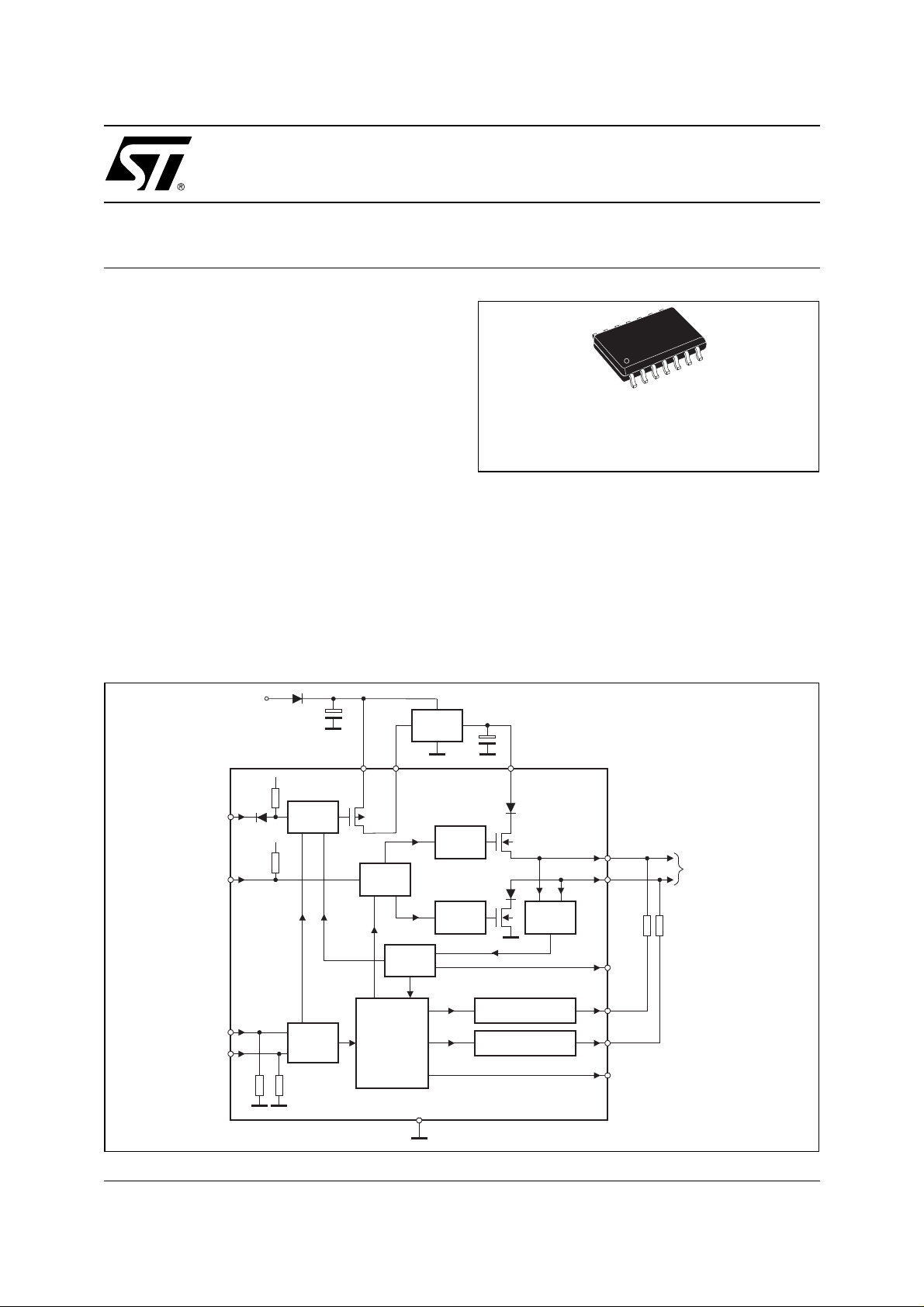
Figure 1. Block Diagram
KL30
(+12V)
5Vint
75k
7
WAKE
VCC
12.5k
2
TXD
5
NSTB
6
EN
99AT0001
Wake-up
Control
Low
Power
Control
100k100k
INHVS
14 1
TXD
Control
Receiver
Error
Management
& Diagnosis
Voltage
Regulator
13
GND
CANH
Driver
CANH
Driver
+5V
VCC
10
Filter
CANH T ermination
CANL T ermination
CANH
11
12
CANL
R
RTH
3
RXD
8
RTH
9
RTL
4
NERR
R
RTL
CAN
BUSLINE
July 2003
1/13
Page 2
L9669
Figure 2. Pin Connection top view.
INH
TXD
RXD
NERR
NSTB
EN
WAKE
99AT0002
1
2
3
4
5
6
7
Table 1. Pin Functions
N° Pin Function
1INH
2TXD
3RXD
4NERR
5NSTB
Inhibit Output
Transmit Data Input
Receive Data Output
Error/Diagnostic Output
Not Standby Input
- for switching external 5V Regulator
- active LOW dominant Bit transmission
- active LOW dominant Bit reception
- Digital control signal for low power modes
- active LOW error/Wake-up and Diagnostic output
14
13
12
11
10
VS
GND
CANL
CANH
VCC
9
RTL
8
RTH
6EN
7 WAKE
8RTH
9RTL
10 VCC
11 CANH
12 CANL
13 GND Ground
14 VS
Enable Input/Diagnostic Clock
Digital control signal for low power modes/Diagnostic clock
Wake-Up Input
switching INH to VS
Termination Resistor for CANH
Termination Resistor for CANL
Supply Voltage Input
High Voltage Bus Line
Low Voltage Bus Line
Battery Voltage Input
- If level of V
- +5V
- High: dominant state
- Low: dominant state
- +12V
-
changes the device initiates a wake-up from sleep mode by
WAKE
- controlled by internal error management
- controlled by internal error management
Table 2. Thermal Data
Symbol Parameter Value Unit
R
thj-amb
Thermal resistance junction to ambient 120 °C/W
2/13
Page 3
Table 3. Absolute Maximum Ratings
For externally applied voltages or currents exceeding these limits damage of the circuit may occur!
Symbol Parameter Value Unit
L9669
V
S-DC
V
S-P
V
CC
V
CANH,L-DC
V
V
WAKE
T
STG
T
Notes: 1. All pins of t he IC are pr otected aga inst ESD. T he verifica tion is perfor med accord ing to MIL 883C, hu man body mo del with
2. Voltage forced means voltage l i m i ted to spec i fied values while current is not l i m i ted. Current force d m eans voltage unlimi t ed but
DC operating battery voltage -0.3 to +28 V
Pulse operating battery voltage (t<400ms) -0.3 to +40 V
Supply voltage -0.3 to +6 V
DC voltage CANH, CANL -28 to +40 V
Voltage TXD, RXD, NERR, NSTB, EN -0.3 to VCC+0.3 V
X
Voltage WAKE -0.3 to VS+0.3 V
Storage temperature -55 to +150
Operating junction temperature -40 to +150
j
R = 1.5kΩ, C = 100pF and discharge vol t age ±2kV, corresponding to a m aximum discharge energy of 0.2mJ.
current li m i ted to specified value.
o
C
o
C
Table 4. Electrical Characteristcs
VCC= 4.75V to 5.25V, VS= 6V to 28V, Tj=-40°C to 150°C unless otherwise specified.
Item Symbol Parameter Test Condition Min. Typ. Max. Unit
1 Supplies
1.1 I
SSL
Supply current in sleep mode
= IVS)
(I
SSL
V
= 0V, VS = 14V 37 65 µA
CC
1.2 I
1.3 I
SSB
SND
Supply current in standby mode
= IVS + I
(I
SSB
Supply current in normal mode
(I
SND
2 CAN Line Interface
2.1 V
Differential receiver recessive to
r-d
dominant threshold
V
CANH
2.2 V
Differential receiver dominant to
d-r
recessive threshold
V
CANH
2.3 V
2.4 V
2.5 V
CANHr
CANHd
CANLr
CANH recessive output voltage V
CANH dominant output voltage V
CANL recessive output voltage V
= IVS + I
- V
CANL
- V
CANL
VCC
VCC
I
= 0 110 160 µA
INH
)
V
= 14V, V
)
S
(dominant state)
TXD
= 0
27 mA
no load at CAN
No bus errors.
= 5V
V
CC
No bus errors.
= 5V
V
CC
= V
TXD
RTH
TXD
TXD
RTH
CC
< 4kΩ
= 0V
= -40mA
= V
CC
< 4kΩ
R
I
CANH
R
-3.50 -2.20 V
-3.85 -2.5 V
0.35 V
VCC-
1.4
VCC-
0.2
V
V
3/13
Page 4

L9669
Table 4. Electrical Characteristcs (continued)
VCC= 4.75V to 5.25V, VS= 6V to 28V, Tj=-40°C to 150°C unless otherwise specified.
Item Symbol Parameter Test Condition Min. Typ. Max. Unit
2.6 V
2.7 I
2.8 I
2.9 I
2.10 I
2.11
V
2.12
2.13 V
2.14 V
2.15
CANLd
CANH
CANL
CANHl
CANLl
CANHWK
V
CANLWK
CANHs
CANLs
V
CANHOV
CANL dominant output voltage V
CANH output current V
CANL output current V
CANH leakage current V
TXD
I
CANL
CANH
V
TXD
CANL
V
TXD
CANH
= 0V
= 40mA
= 0V
= 0V
= 5V
= 0V
= 14V
1.4 V
-160 -110 -70 mA
70 110 160 mA
0 µA
Sleep mode.
CANL leakage current V
CANL
= 0V
0 µA
Sleep mode.
CANH wake-up voltage Sleep/standby mode. 1.2 1.9 2.7 V
CANL wake-up voltage Sleep/standby mode. 2.4 3.1 3.8 V
CANH single ended receiver
threshold
CANL single ended receiver
threshold
CANH overvoltage detection
threshold
Normal mode.
= 5V
V
CC
Normal mode.
= 5V
V
CC
Normal mode.
= 5V
V
CC
1.5 1.8 2.15 V
2.7 3.1 3.4 V
7.2 V
2.16 V
CANLOV
2.17 t
2.18 t
2.19 t
2.20 t
2.21 t
wuCAN
2.22 t
drd
ddr
r,f
r,f
wuWK
CANL overvoltage detection
threshold
Propagation delay
TXD to RXD
recessive to dominant
Propagation delay
TXD to RXD
recessive to dominant
CANH, CANL output
rise/fall time
dominant to recessive
CANH, CANL output
rise/fall time
dominant to recessive
Minimum dominant time for
wake-up on CANH or CANL
Minimum pulse time for
wake-up on WAKE
Normal mode.
= 5V
V
CC
10% to 90%
= C2 = 3.3nF
C
1
7.2 V
1 1.6 µs
R1 = 100Ω
10% to 90%
= C2 = 3.3nF
C
1
2.2 µs
R1 = 100Ω
10% to 90%
= C2 = 3.3nF
C
1
0.6 1.5 µs
R1 = 100Ω
10% to 90%
= C2 = 3.3nF
C
1
2.6 6 µs
R1 = 100Ω
Sleep/standby mode. 8 44 µs
Sleep/standby mode 4 44 µs
4/13
Page 5

Table 4. Electrical Characteristcs (continued)
VCC= 4.75V to 5.25V, VS= 6V to 28V, Tj=-40°C to 150°C unless otherwise specified.
Item Symbol Parameter Test Condition Min. Typ. Max. Unit
3 Termination RTH, RTL
L9669
3.1 R
3.2 I
3.3 R
3.4 I
3.5 R
3.6 V
3.7 R
RTH
RTH
RTL
RTL
RTL-VS
RTH
RTH,
RTL
4 Input TXD
4.1 V
TXDh
Internal RTHto GND
switch-on resistance
Internal RTHto GND
pull down current
Internal RTLto VCC
switch-on resistance
Internal RTLto VCC
pull up current
Internal RTLto VS
termination resistance
Normal mode.
No errors.
= 1V
V
RTH
Normal mode.
Error 3.
= 1V
V
RTH
Normal mode.
No errors.
= VCC - 1V
V
RTL
Normal mode.
Error 4, 6 or 7.
= VCC - 1.5V
V
RTL
Sleep/standby mode.
= 1V, 5V
V
RTL
81326kΩ
RTH output voltage Sleep/stan dby mode
= 1mA
I
RTH
External termination resistance 0.5 16 kΩ
TXD high level input voltage VCC-
45 Ω
75 µA
45 Ω
-75 µA
1V
V
CC
0.9
V
4.2 V
4.3 I
4.4 I
TXDl
TXDh
TXDl
TXD low level input voltage 0 0.9 V
TXD high level input current V
TXD low level input current V
5 Outputs RXD, NERR
5.1 V
5.2 V
High level output voltage VCC-
Xh
Low level output voltage 0 0.9 V
Xl
6 Output INH
6.1 V
6.2 I
dropI
High level voltage drop
= VS - V
(V
dropI
Leakage current V
Il
INH
= 4 V -200 -25 µA
TXD
= 1 V -800 -100 µA
TXD
V
CC
V
0.9
I
= -0.18mA
)
INH
Not sleep mode.
= 0V
INH
-5 5 µA
1V
Sleep mode.
5/13
Page 6

L9669
Table 4. Electrical Characteristcs (continued)
VCC= 4.75V to 5.25V, VS= 6V to 28V, Tj=-40°C to 150°C unless otherwise specified.
Item Symbol Parameter Test Condition Min. Typ. Max. Unit
7 Inputs NSTB, EN
7.1 V
7.2 V
7.3 I
7.4 I
High level input voltage VCC-
Xh
Low level input voltage 0 0.9 V
Xl
High level input current VX = 4 V 10 150 µA
Xh
Low level input current VX = 1 V 2 40 µA
Xl
8 Input WAKE
8.1 V
8.2 V
WAKEh
WAKEl
WAKE high level input voltage 3 V
WAKE low level input voltage 0 0.9 V
9 Thermal shutdown
9.1 T
Shutdown junction temperature 170 °C
jsd
10 CAN Error detection
10.1 t
10.2 t
10.3 t
fail38d
fail46710d
fail38r
Error 3, 8 detection time Normal/RXonly mode. 1.6 3.6 ms
Error 4, 6, 7, 10 detection time Normal/RXonly mode. 0.4 1.6 ms
Error 3, 8 recovery time Normal/RXonly mode. 0.4 1.6 ms
0.9
V
CC
S
V
V
10.4 t
10.5 t
10.6 t
10.7 t
10.8 t
10.9 t
10.10 N
10.11 N
10.12 t
10.13 t
6/13
fail47r
fail6r
fail10r
fail38ds
fail4rs
fail348rs
edge-d
edge-r
Dmax
Hmin
Error 4, 7 recovery time Normal/RXonly mode. 10 50 µs
Error 6 recovery time Normal/RXonly mode. 0.2 0.75 ms
Error 10 recovery time Normal/RXonly mode. 0.7 4 µs
Error 3, 8 detection time Sleep/standby mode. 1.6 3.6 ms
Error 4 recovery time Sleep/standby mode. 0.4 1.6 ms
Error 3, 4, 8 recovery time Sleep/standby mode. 0.4 1.6 ms
Edge count difference between
CANH and CANL for detection
Edge count difference between
CANH and CANL for recovery
Normal/RXonly mode.
Error 1, 2, 5 or 9.
Normal/RXonly mode.
Error 1, 2, 5 or 9.
3 Edges
3 Edges
Diagnostic timeout 15 80 µs
minimum hold time
80 µs
go to sleep
Page 7

L9669
1. FUNCTIONAL DESCRIPTION
The L9669 is a monolithic integrated circuit which provides all main functions for an automotive body CAN system. The device guarantees a clearly defined behavior in case of failure to avoid permanent CAN bus errors. It
is primarily intended for low speed applications in passenger cars.
1.1 Transceiver
– Supports double wire unshielded busses
– Baud rates up to 125 kBaud
– Single wire operation possible (automatic switching to single wire upon bus failures)
– Bus not loaded in case of unpowered transceiver
The CAN transceiver st age is able to t ransfer ser ial data on two independ ent communi cation w ires e ither differentially (normal operation) or in case of a single wire fault on the remaining line. The physical bitcoding is done
using dominant (transmitter active) and overwritable recessive states. Too long dominant phases are detected
internally and further transmission is automatically disabled (malfunction of protocol unit does not affect communication on the bus (“fail safe mechanism”)).
1.2 Modes of Operation
Five different functional modes exist to enable or establish the usage of low power or receive only operation.
NSTB EN Mode INH NERR RXD RTL
0 0 standby VS
0 0 sleep
0 1 “go to sleep”
floating
active LOW wake-up interrupt signal
(if VCC is present)
switched to VS
(typ. 13kΩ)
1 1 normal
RXonly
VS
10
Power on
Note: Wake-up interrupts are released when entering RXonly or normal mode.
active LOW
error flag
active LOW
VS power-on
flag if VCC is
present
HIGH=recessi ve
LOW=dominant
received data
active LOW
wake-up interrupt
signal if VCC is
present
switched to VCC
switched to VS
The following state diagr am sh ows these modes and the po ssibl e state i nter actions depending on the input signals NSTB and EN.
7/13
Page 8

L9669
Figure 3.
NSTB = 1
EN = 0
NSTB = 0
EN = 0
Standby Mode
NSTB EN INH
00VS
NSTB = 0
EN = 1
NSTB = 1
EN = 0
NSTB = 0
EN = 0
NSTB = 1
EN = 1
Power on
Mode
RX only
Mode
NSTB EN INH
10
99AT0003
VS
NSTB = 0
EN = 1
"Go to Sleep" Mode
NSTB EN INH
0 1 Float.
NSTB = 0
EN = 0
Sleep Mode
NSTB EN INH
0 0 Float.
NSTB = 0
EN = 1
Normal Mode
NSTB EN INH
11VS
Wake-up
8/13
Page 9

L9669
1.3 Error Mana g em e nt
Ten different errors on the physical buslines can be distinguished:
N Type of Errors
Errors caused by damage of the datalines or isolation
1 CANH wire interrupted (floating or tied to termination) 0 0
2 CANL wire interrupted (floating or tied to termination) 0 0
3 CANH short circuit to VS (overvoltage condition) 1 1
4 CANL short circuit to GND (permanently dominant) 2 0
5 CANH short circuit to GND (permanently recessive) 0 2
6 CANL short circuit to VS (overvoltage condition) 1 1
7 CANL shorted to CANH 2 2
Errors caused by misbehaviour of transceiver stage
8 CANH short circuit to VCC (permanently dominant) 2 0
9 CANL short circuit to VCC (permanently recessive) 0 2
Errors caused by defective protocol unit
10 CANH, CANL driven dominant for more than 1.3 ms 2 2
Not all of these errors leads to a breakdown of the whole communication. S o the errors can be categorized into
“negligible” (severity 0), “problematic” (severity 1) and “severe” (severity 2).
Severity
RX TX
Negligible Errors
Transmitter
Error 1, 2, 4 or 8: In all cases data still can be transmitted in differential mode.
Receiver
Error 1, 2, 5 or 9: In all cases data still can be received in differential mode.
Prob le m a t ic Erro rs
Transmitter
Error 3 or 6: Data are transmitted using the remaining dataline (single wire).
Receiver
Error 3 or 6: Data are received using the remaining dataline (single wire).
Severe Errors
Transmitter
Error 5 or 9: Data are transmitted using the remaining dataline after short circuit detection.
Error 7: Data are transmitted on CANH or CANL after overcurrent was detected.
Error 10: Transmission is terminated (fail safe).
Receiver
Error 7: Data are received on CANH or CANL after detection of permanent dominant state.
Error 4 or 8: Data are received on CANH or CANL after short circuit was detected.
Error 10: Data are received normally, error is detected by protocol unit.
Upon any e rror i n nor mal or RXonly mode th e NERR output w ill be forced LOW and rel eased af ter erro r recover y.
9/13
Page 10

L9669
1.4 Diagn osis
A serial interface i s avai lable to retriev e diagnosti c informatio ns. Di agnostic data can be reques ted by usi ng EN
as serial clock and evaluating NERR.
Figure 4.
NSTB
EN
t
Dmax
No Bus Errors
99AT0004
Bus Error
NERR
Mode
(Example)
detected
E1
or E5E2or E9
Normal RXonly Standby
Delay between falling slope at EN and reaction at NERR: 0.7µs...3.0µs
(NERR is synchronized with internal clock).
E3 E4
Diagnosis
Readout is initialized by a negative edge on EN and acknowledged by NERR entering HIGH state. Following
the next negative edge the first error status bit is displayed on NERR according to the data table below. If no
edge on EN is detected fo r a time longer tha n t
diagnosis is disabled and oper ation c ontinuous in the mode
Dmax
given by NSTB and EN with NERR showing bus errors or wake-up correspondingly. If the clock continues, the
readout sequence starts over again with the initial bit set HIGH.
The following errors are displayable (sequence listed in chronological order):
– error status bit 1 (LSB): HIGH if Error 1 or 5
– error status bit 2: HIGH if Error 2 or 9
– error status bit 3: HIGH if Error 3
– error status bit 4: HIGH if Error 4
– error status bit 5: HIGH if Error 6
– error status bit 6: HIGH if Error 8
– error status bit 7: HIGH if Error 10
– error status bit 8: HIGH if Thermal shutdown of Transceiver
1.5 Protections
A current limiting circuit protects the transmitter outputs against short-circuit to battery, ground and shorted
wires.
If the junction temperature exceeds a maximum value, the transmitter output stages are disabled.
10/13
Page 11

2. APPLICATION CIRCUIT DIAGRAM
Figure 5.
CAN
BUS
LINE
7
L9669
KL30 (+12V)
WAKE
99AT0005
RTH
8
R
RTH
CANH
11
CANL
12
R
RTL
RTL
9
CAN
Transceiver
13
GND
14
1
10
2
3
4
5
6
3. TEST CIRCUIT FOR DYNAMIC CHARACTERISTICS
Figure 6.
+5V
+14V
VS
INH
VCC
TXD
RXD
NERR
NSTB
EN
+5V
CAN
Controller
Voltage
Regulator
99AT0006
NSTB
EN
WAKE
TXD
NERR
5
6
7
2
4
20pF
INH VS
14 10
1
3
RXD GND
13
VCC
12
11
9
8
RTL
CANL
CANH
RTH
R
1
R
1
C
1
C
2
C
1
11/13
Page 12

L9669
DIM.
MIN.. TYP. MAX.. MIN.. TYP.. MAX..
A 1.75 0.069
a1 0.1 0.25 0.004 0.009
a2 1.6 0.063
b 0.35 0.46 0.014 0.018
b1 0.19 0.25 0.007 0.010
C 0.5 0.020
c1 45˚ (typ.)
D (1) 8.55 8.75 0.336 0.344
E 5.8 6.2 0.228 0.244
e 1.27 0.050
e3 7.62 0.300
F (1) 3.8 4 0.150 0.157
G 4.6 5.3 0.181 0.209
L 0.4 1.27 0.016 0.050
M 0 .68 0.027
S8˚
(1) D and F do not include mold flash or protrusions. Mold flash or
potrusions shall not exceed 0.15mm (.006inch).
mm inch
(max.)
OUTLINE AND
MECHANICAL DATA
SO14
12/13
Page 13

L9669
Information furnished is believed to be accurate and reliable. However, STMicroelectronics assumes no responsibility for the consequences
of use of such information nor for any infringement of patents or other rights of third parties which may result from its use. No license is granted
by implic ation or otherwise unde r any patent or patent rights of STMicroelectroni cs. Specifications me nt i oned in this publication are subject
to change without notice. This publication supersedes and replaces all information previously supplied. STMicroelectronics produ ct s are not
authorized for use as crit i cal component s in l i fe support dev i ces or systems without express written approval of STMic roelectronics.
The ST logo is a registered trademark of STMicroelectronics
2003 STMicroelectroni cs - All Rights Reserved
Austra lia - Brazil - Can ada - China - Finl and - France - Germ any - Hong Kong - India - Israel - I taly - Japan -Malaysia - Mal ta - Morocco -
Singap ore - Spain - Sweden - Switzerl and - United Ki ngdom - United S tates.
STMicroelectronics GROUP OF COMPANIES
http://www.s t. com
13/13
 Loading...