

Page 1
■
Modified VDMOS Power Stage (U
■
RDSON < 500 mOhm (Tj = 25°C)
■
CMOS Compatible Inputs
■
Enable Input (Reset)
■
Outputs Capable of up to 2.2 Amperes
■
Outputs Internally Clamped at 70V for Fast
DSBR
> 80V)
Inductive Load Switch Off
■
Wide operating supply voltage from 4.7V up to
30V
DIAGNO STIC FUNCTIONS
■
Open Load Detection (Output off, 100µsfiltering time)
■
Short to Ground Detection (Output off, 100µs filtering time)
■
Short to Battery Detection (Output on)
■
Over temperature detection (Output on)
■
Storage of last fault in 8 Bit - Serial Register
■
Fault Signal Indication at Serial Data Out
without need to read out the Serial Interface
■
Daisy Chainable Serial Diagnostic
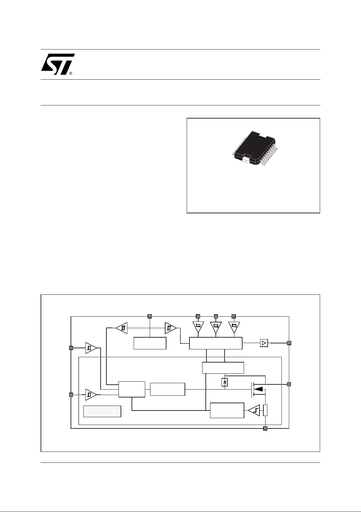
L9651
SMART QUAD SWITCH
PowerSO-20
ORDERING NUMBER: L9651
■
Serial Interface Clock Frequency up to 500kHz
DESCRIPTION
The L9651 consists of four identical low side power
switches. A serial diagnostic interface indicates failure mode of each switch (short circuit to V
ground and open load or over temperature).
BAT
or
BLOCK DIAGRAM
Reset
Inputs 1..4
April 2001
Four Fold
Turn On
Logic
V
BAT
Underv. Shutd.
●
References
Control
Gate
Data In
Clock Sync.
Serial Diagnostic
Fault Detection
Short Circuit
●
●
●
Protection
Serial Data Out
●
●
Output 1..4
Ground
1/9
Page 2
L9651
PIN CONNECTION
(Top view)
GND
N.C.
IN1
IN2
OUT1
VBAT
OUT2
DO
CL
1
2
3
4
5
6
7
8
9
GND 10
SO20POW
PIN FUNCTION
N° Pin Function
20
19
18
17
16
15
14
13
12
11
GND
N.C.
IN4
IN3
OUT4
R
OUT3
DI
SY
GND
1, 10,
11, 20
2, 19 N.C. Not Connected
3 IN1 Input 1
4 IN2 Input 2
5 OUT1 Output 1
6 VBAT Supply Voltage
7 OUT2 Output 2
8 DO Serial Data Out
9 CL Clock
12 SY Synchronization
13 DI Serial Data In
14 OUT3 Output 3
15 R Reset
16 OUT4 Output 4
17 IN3 Input 3
18 IN4 Input 4
GND Ground
2/9
Page 3
ABSOLUTE MAXIMUM RATINGS
Symbol Parameter Value Unit
L9651
V
VR,V
VCLV
T
STG
T
V
BA T
V
BATtr
V
OUT
OUTtr
E
CL
-I
OUT
INi,VDI,
V
DO
Storage Temperature -55 to 150
Operating Junction Temperature -40 to 150
J
DC Supply Voltage -2 to 30 V
Transient Supply Voltage; t < 400ms 40 V
Output Voltage 65 V
Transient Output Voltage; during clamping 78 V
Output Clamping energy; repetition rate < 100 Hz 10 mJ
Output reverse current 2 A
Control Input voltage -0.3 to 6.5 V
SY
Control Output voltage -0.3 to 6.5 V
THERMAL DATA
Symbol Parameter Value Unit
R
th j-case
Thermal Resistance Junction to Case 2.5 °C/W
o
C
o
C
ELECTRICAL CHARACTERISTCS
(6.5V < V
< 25V, -40 < TJ < 150°C)
BAT
Symbol Parameter Test Condition Min. Typ. Max. Unit
Supply Voltage
V
BATU
I
BA T
Turn on threshold voltage 2.0 4.7 V
Supply current V
V
BAT
OUTi
= 14V
> 0V
41015mA
Output stage
R
DSON
V
On resistance V
Clamping voltage,
CL
= 14V
BAT
T
= 25°C; I
J
= 14V
V
BAT
T
= 150°C; I
J
I
= 0.5 A 63 70 76 V
out
out
= 1A
out
= 1A
500
850
inductive load
I
OUTi
Over current shutdown
= -40°C
T
J
3.0
4.3
(Shutdown latch resets
with pos. slope at INi)
= 25°C
T
J
= 150°C
T
J
2.5
2.2
3.7
3.5
Output leakage current see: Open load diagnostic current
mΩ
mΩ
A
A
A
3/9
Page 4

L9651
ELECTRICAL CHARACTERISTCS
(continued)
Symbol Parameter Test Condition Min. Typ. Max. Unit
Logic Inputs
V
INiLH
V
SYLH
V
CLLH
V
RLH
V
DILH
V
INiHL
V
SYHL
V
CLHL
V
RHL
V
DIHL
V
INih
V
SYh
V
CLh
V
Rh
V
DIh
- I
INi
- I
SY
- I
C L
- I
R
- I
DI
IN1...IN4, SY, CL, DI, R
Input High level 3.5 6.5 V
Input Low level -0.3 1.5 V
Hysteresis 0.2 1 V
Input current IN1 ... IN4, SY, CL, R
(Internal pull up current source)
V
= 0V 10 40 120 µA
INi
V
SY
= 0V
10 80
VCL = 0V
VR = 0V
Input current DI
VDI = 0V 120 220 250 µA
(Internal pull up current source)
Timing
t
don
t
doff
s
s
t
f
t
vDV
t
vset
t
vhold
Turn on delay 7.5 µs
Turn off delay 7.5 µs
Switch on slew rate 10 V/µs
on
Switch off slew rate 15 V/µs
off
Over current detection time 0.5 µs
oc
t
Open load filtering time 60 100 20 0 µs
v
t
Short to GND filtering time 60 100 200 µs
v
Serial clock frequency 0 500 kHz
CL
DO: Datavalidtime 0.03 1 µs
DI: Datasettlingtime 0.5 µs
DI: Dataholdtime 0 µs
Diagnostic
V
BA TDU
Under voltage threshold 4.7 7.5 V
Serial Data output (External pull up required)
V
| I
Data output low voltage IDO < 1.6mA
DO
| Data output leakage current 10 µA
DO
7.5V < V
BA T
< 22V
00.45V
4/9
Page 5

L9651
ELECTRICAL CHARACTERISTCS
(continued)
Symbol Parameter Test Condition Min. Typ. Max. Unit
Output voltage monitoring Output off
V
V
Open load threshold voltage
OL
(fault detected if V
Short to GND threshold voltage
SG
(fault detected if V
OUTi
OUTi
< VOL)
< VSG)
7.5V < V
7.5V < V
BA T
BA T
< 22V
< 22V
2/3V
1/3V
BA T
BA T
Open load diagnostic current Output off
- I
I
OUTi
OUTi
Open load output voltage I
Output current V
Output current V
= 0 A
OUT
V
= 5V
INi
7.5V < V
= 1V
OUT
V
= 5V
INi
= V
OUT
V
= 5V
INi
7.5V < V
BA T
BAT
BA T
< 22V
< 22V
1/2V
BA T
50 100 150 µA
200 320 500 µA
Overload Diagnostic
I
OUTi
Over temperature diagnostic T
J
Over current TJ = -40°C
= 25°C
T
J
3.0
2.5
175 °C
4.3
3.7
A
A
= 150°C
T
J
Figure 1. Typical Timing Diagram for Serial Diagnostic
Fault: Short to Battery o r over temp.
F ault: Open Load or Short to GN D
o. k.
o. k.
DI
SY
CL
DO
< t
v
H
L
Di1 Di2 Di3
H
L
t
vset
H
L
H
L
t
v
Bit1 Bit2
Bit3 Bit4
t
vhold
Bit5 Bit7 Bit8Bit6
t
vDV
1/f
2.2
CL
Di1 Di2
Di3
3.5
A
Shift R egister D ata Froze n
Reset of Shift Register
5/9
Page 6

L9651
Figure 2. Serial Interface Error Coding
BIT 1
OUTPUT 1
BIT 2
BIT 4
BIT 3
OUTPUT 2
H
H
LH
L
H
LL
BIT 5 BIT 6
OUTPUT 3
o.k.
open load/over temperature
short to ba tte ry
short to ground
Figure 3. Output voltage TIMING for inductive load
BIT 7 BIT 8
OUTPUT 4
BIT n
DI
6/9
0.8V
0.8V
0.2V
V
V
V
BA T
BA
V
V
INiH
V
INiL
OUTi
CL
BAT
INi
t
CL
s
OFF
s
ON
T
td
on
td
off
t
Page 7

Figure 4. Application Circuit
L9651
V
BAT
●
5 Volt
Regulator
V
●
Controller
●●●●
CC
●
RESET
●
●
●
●
RR
IN1
IN2
IN3
IN4
DO
●
SY
OUT1
●
OUT2
OUT3
OUT4
DI
CL
●
●
●
●
●
●
Further
driver ICs
with
4-Wire-
DO
SY
Diagnostic
CL
●
R
DI
7/9
Page 8

L9651
DIM.
MIN. TYP. MAX. MIN. TYP. MAX.
mm inch
A 3.6 0.142
a1 0.1 0.3 0.004 0.012
a2 3.3 0.130
a3 0 0.1 0.000 0.004
b 0.4 0.53 0.016 0.021
c 0.23 0.32 0.009 0.013
D (1) 15.8 16 0.622 0.630
D1 9.4 9.8 0.370 0.386
E 13.9 14.5 0.547 0.570
e 1.27 0.050
e3 11.43 0.450
E1 (1) 10.9 11.1 0.429 0.437
E2 2.9 0.114
E3 5.8 6.2 0.228 0.244
G 0 0.1 0.000 0 .004
H 15.5 15.9 0.610 0.626
h 1.1 0.043
L 0.8 1.1 0.031 0.043
N 10˚ (max.)
S
8˚ (max.)
T10 0.394
(1) "D and F" do not include mold flash or protrusions.
- Mold flash or protrusions shall not exceed 0.15 mm (0.006").
- Critical dimensions: "E", "G" and "a3"
OUTLINE AND
MECHANICAL DATA
JEDEC MO-166
PowerSO20
E2
h x 45
DETAIL B
BOTTOM VIEW
R
lead
a3
Gage Plane
E
DETAIL B
0.35
S
D1
L
c
a1
DETAIL A
slug
- C -
SEATING PLANE
GC
(COPLANARITY)
E3
NN
a2
A
b
DETAIL A
e3
H
D
T
1
e
1120
E1
10
PSO20MEC
8/9
Page 9

L9651
Information furnished is believed to be accurate and reliable. However, STMicroelectronics assumes no responsibility for the consequences
of use of such information nor for any infringement of patents or other rights of third parties which may result from its use. No license is granted
by implic ation or otherwise unde r any patent or patent rights of STMicroelectroni cs. Specifications me ntioned in th i s publication are subject
to change without notice. This publication supersedes and replaces all information previously supplied. STMicroelectronics produ ct s are not
authorized for use as crit i cal component s in l i fe support dev i ces or systems without express written approval of STMic roelectronics.
The ST logo is a registered trademark of STMicroelectronics
2001 STMi croelectroni cs - All Rights Reserved
Australi a - Brazil - China - Finland - France - Ger many - Hong Kong - India - Italy - Japan - Malaysia - Malta - Mo rocco - Singa pore - Spain
STMicroelectronics GROUP OF COMPANIES
- Sweden - Sw itzerland - United Kingdo m - U.S.A.
http://www.s t. com
9/9
 Loading...