

Page 1
BIDIRECTIONALSWITCH
MOTOR STOP CONTROLLED BY MOTOR
CURRENT
START UP AND END CURRENT DETEC-
TION THRESHOLDS PROGRAMMABLE
WITH EXTERNALRSHUNT
STOP DELAY TIME FOR START UP AND
END PHASE PROGRAMMABLE WITH EXTERNAL RC
OUTPUTSHORTCIRCUITPROTECTION
OUTPUTCURRENT LIMITING > 8A
THERMALPROTECTION
ACTIVE DIODE BRIDGE INTERNALLY DIF-
FUSED
MAXIMUMVOLTAGESUPPLY50V
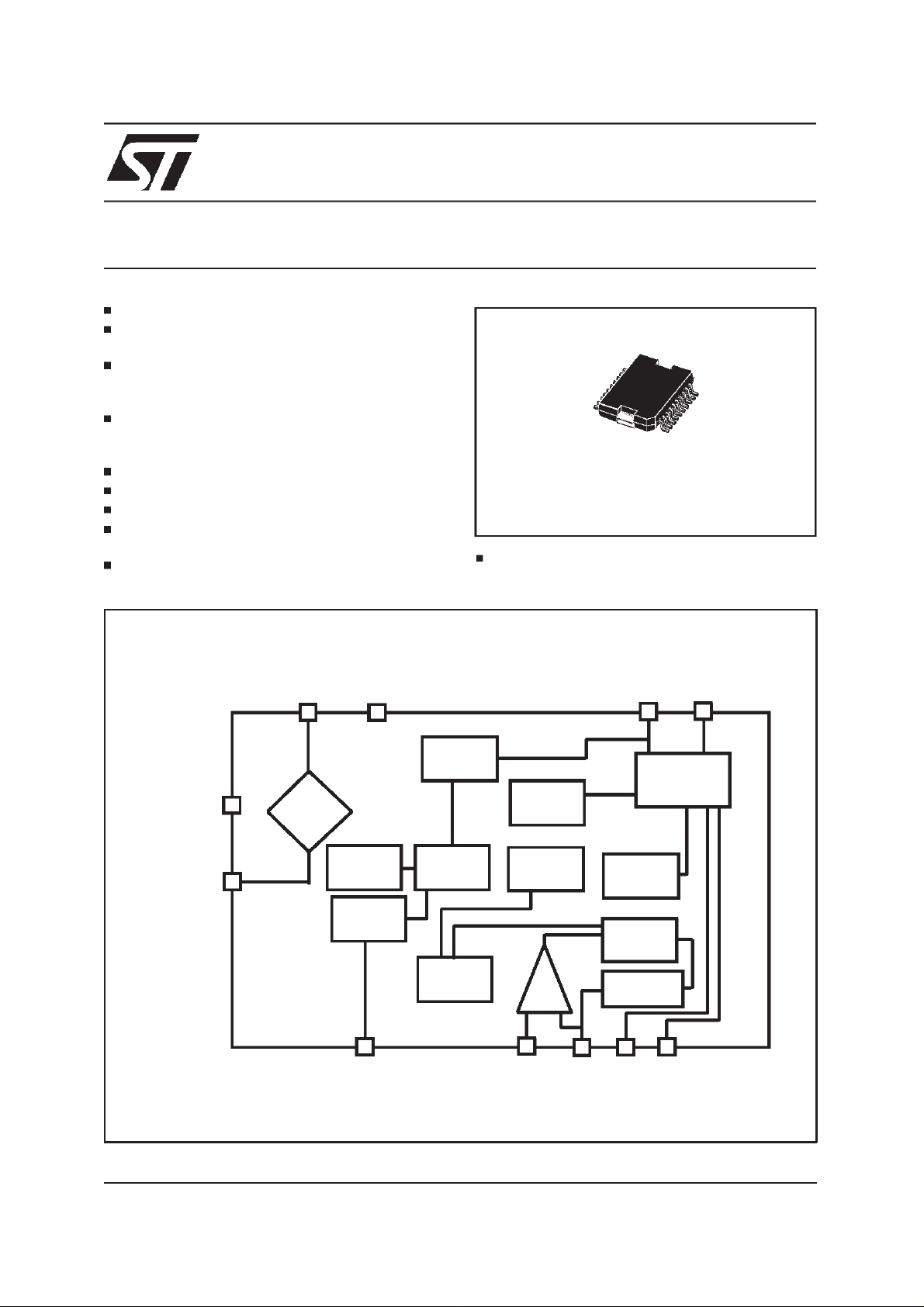
BLOCK DIAGRAM
L9639
FOLDER ACTUATOR
PowerSO20
TECHNOLOGYMULTIPOWERBCD60II
GND
1,10,11,20
LIVE
2
COMMON
19
ACTIVE
BRIDGE
V+
14
POWER ON
RESET
CHARGE
CEX.
8
RCEX
OPEN LOAD
DETECTOR
CHARGE
PUMP
LOGIC HV REF.
VOLTAGE
THERMAL
PROTECT.
VREF S H U N T
COMP.
17
CURRENT
PROTECT.
CONTROL
LOGIC LV
REF.COMP.
CURRENT
5346
16
POWER
DUAL DMOS
November 1998
1/6
Page 2
L9639
ABSOLUTE MAXIMUM RATINGS
Symbol Parameter Value Unit
V
bat
I
out
T
op
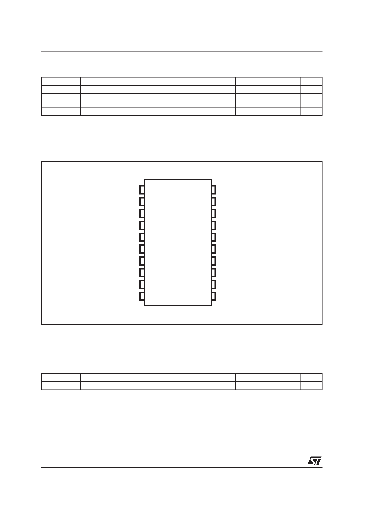
PIN CONNECTION
Supply Voltage 50 V
Output current DC
at Is
Operating Temperature -40 to 125 °C
5
6
A
A
THERMAL DATA
GND
LIVE COMMON
SHUNT
SHUNT
SHUNT
VREF
NC
RCEX
GND
1
2
3
4
5
6
7
8
9
10
20
19
18
17
16
15
14
13
12
11
GND
NC
OUT
OUT
NC
V+
NC
NCNC
GND
Symbol Parameter Value Unit
Thermal Resistance Junction to case Max. 4 °C/W
2/6
R
th j-case
Page 3

ELECTRICALCHARACTERISTICS (Refer to the test circuit,unlessotherwisespecified.)
Symbol Parameter Test Condition Min. Typ. Max. Unit
V
bat
I
q
I
ref
I
refcc
I
sc1
T
dsc
R
on
R
ona
R
load
K
td
Deb Immunity debouncer switch V
Power supply 8 17 V
Quiescent current Stanby 100 200
Current ref. threshold for start
V
= 8 to 17V 70 100 135
bat
and end current (note 1)
Current ref. threshold for short
circuit current det (note 2)
Vbat = 8V
V
= 12V
bat
V
= 17V
bat
240
300
400
300
440
550
400
560
690
Current short circuit limit 8 A
Short circuit time delay I
Ronoutput power DMOS I
Ronactive bridge DMOS V
Open load detector max. load
load>Ithcc
= 1.2A 0.6 1 Ohm
load
bat
= 8V, I
= 1A 0.7 Ohm
gnd
100
200 Ohm
resistance
Delay constant (note 3) 1
= pulse
bat
L9639
A
µ
A
µ
A
µ
s
µ
thcc
d
R_ref
R
=
=
shunt
R_ref
R
In
shunt
V
V
I
ref
⋅ I
refcc
th_high
Rex⋅Cex=Rex⋅Cex⋅Ktd
⋅
th_low
Note 1: Ith=
Note 2: I
Note 3: T
DESCRIPTION
This device typically drives a direct current motor
servomechanismprovidingtwoextremeend positions and replaces end position switches or sensors.
For more details see the Timing diagram (Fig. 1)
and the Applicationdiagram(Fig. 2)
When the power supply is applied, or its polarity
is inverted the motor is powered up (start point).
The current of the motor reaches the start up
value near to the stall current, always higher than
the threshold value of the device (I
on the detection (T
) permits the motor start up
D
) . A delay
TH
and the consequentdecrease of the current.
During the free running phase, the current in the
motor must always be lower the threshold I
TH
When the motor reaches the end of the run limit,
the current increases reaching a value that, depending on the application, can be the stall value
or can depend on some torque limiting friction
(end point). Provided that this value is higher the
programmed threshold I
after a time delay T
D
, the motor is stopped
TH
, and the device goes into a
low consumption standby status, ready to restart
the motor for a new cycle if the polarity of the
power supply is inverted (or power is switched off
and on).
In any case, if the current exceeds the higher
thresholdI
, the motor is immediatelystopped
THCC
because a short circuit is detected. The delay T
also permits the motor to overcome some small
obstacleduring the free run.
The threshold current for the runningphase I
obtained by comparingthe voltage on an external
sensing resistor (R
.
V
TH
1) I
TH=VTH/RSHUNT
) to a threshold voltage
SHUNT
VTHis constant in respect to the power supply
voltage because in most applications, the end of
run current is depending only on motor and the
mechanictorque limiting device (friction current).
The threshold current for the short circuit detection is:
2) I
THCC=VTHCC/RSHUNT
V
= 12V
.
bat
and depends intentionally on the supply voltage
@V
THCC
= 330mV@
because of the same dependenceof the stall current. The time T
ponents, capacitor C
depends on two external com-
D
and resistor REX.TDis
EX
obtained by thefollowingexpression:
T
D=REX
R
EX
K
⋅
TD
⋅
KTDisa constanttypicallyof unitvalue.
The block diagram is shown on the first page.
The change of the polarity between pins COMMON and LIVE,needs the active bridge to supply
the internal circuit. The internal supply voltage is
available between pins V+ and GND and a storage and filter capacitor (100nF) must be connected between these pins. The output stage
D
TH
is
3/6
Page 4

L9639
consists of two DMOS transistors connected in
series with common drain to act as a switch with
the voltage applied in both direction. A charge
pump takes the gates of the DMOS above the
Figure 1. Functional timing diagram.
ITHCC
3
2
ITH
1
VTH_HIGH
STALLCURRENT 2.3A FRICTION
Figure 2. Applicationschematic diagram.
supply voltage. The motor is controlled by the
control ’logic low voltage’ block that receives the
motor status for the comparator.The ’charge C
block controls the T
delay.
D
1.2A
VTH_LOW
EX
’
GND
NC
OUT
OUT
NC
V+
NC
NCNC
GND
M
C+
R_SHUNT
R_REF
R_EX
C_EX
GND
LIVE COMMON
SHUNT
SHUNT
SHUNT
VREF
NC
RCEX
GND
All the necessaryexternal components are shown in the applicationdiagram. It is importantto shunt the
motor with a devicethat limits the maximum over voltageto 40V. This is necessarywhen the powersupply circuit is opened on motor power up. In this case the back E.M.F. must be clamped becausethere is
no otherfree wheel current path.
4/6
Page 5

L9639
DIM.
MIN. TYP. MAX. MIN. TYP. MAX.
mm inch
A 3.6 0.142
a1 0.1 0.3 0.004
a2 3.3
0.012
0.130
a3 0 0.1 0.000 0.004
b 0.4 0.53 0.016 0.021
c 0.23 0.32 0.009 0.013
D (1) 15.8 16 0.622 0.630
D1 9.4 9.8 0.370 0.386
E 13.9 14.5 0.547 0.570
e 1.27 0.050
e3 11.43 0.450
E1 (1) 10.9 11.1 0.429 0.437
E2 2.9
0.114
E3 5.8 6.2 0.228 0.244
G 0 0.1 0.000 0.004
H 15.5 15.9 0.610 0.626
h 1.1
0.043
L 0.8 1.1 0.031 0.043
N10°(max.)
S
8°(max.)
T 10 0.394
(1)”D andF” donot include mold flashor protrusions.
- Moldflash orprotrusions shallnot exceed0.15 mm (0.006”).
- Criticaldimensions: ”E”,”G” and”a3”
OUTLINE AND
MECHANICAL DATA
JEDEC MO-166
PowerSO20
E2
hx
45
DETAIL B
BOTTOM VIEW
R
a3
Gage Plane
lead
E
DETAIL B
0.35
S
D1
a1
L
c
DETAIL A
slug
-C-
SEATING PLANE
GC
(COPLANARITY)
E3
NN
a2
A
b
DETAIL A
e3
H
D
T
1
e
1120
E1
10
PSO20MEC
5/6
Page 6

L9639
Information furnished is believed to be accurate and reliable. However, STMicroelectronics assumes no responsibility for the consequences
of use of such information nor for any infringement of patents or other rights of third parties which may result from its use. No license is
granted by implication or otherwise under any patent or patent rights of STMicroelectronics. Specification mentioned in this publication are
subject to change without notice. This publication supersedes and replaces all information previously supplied. STMicroelectronics products
are not authorized for use as criticalcomponents in life support devices or systems without express written approval ofSTMicroelectronics.
The ST logo is a registeredtrademark of STMicroelectronics
1998 STMicroelectronics – Printedin Italy – All Rights Reserved
STMicroelectronics GROUP OF COMPANIES
Australia - Brazil - Canada - China- France - Germany - Italy - Japan - Korea- Malaysia - Malta - Mexico - Morocco - The Netherlands-
Singapore- Spain - Sweden- Switzerland- Taiwan - Thailand - United Kingdom- U.S.A.
http://www.st.com
6/6
 Loading...