

Page 1
L9615 MEETS ISO/DIS 11898 UP TO
500KBAUD
TRANSMITTER
- GENERATION OF DIFFERENTIAL OUTPUT
SIGNALS
- SHORT CIRCUIT PROTECTED FROM -5V
TO 36V, DETECTION & SHUTDOWN
- SLOP E CONT ROL T O REDU CE RF I AND E MI
- TWO STAT ES ADJUST A BL E SL O P E
CONTROL (≤500KBAUD/≤125KBAUD)
RECEIVER
- DIFFERENZIAL INPUT WITH HIGH
INTERFERENCE SUPPRESSION
- COMMON MODE INPUT VOLTAGE RANGE
(V
) FROM -2V TO VS+3V
COM
PACKAGE: SO 8
DESCRIPTION
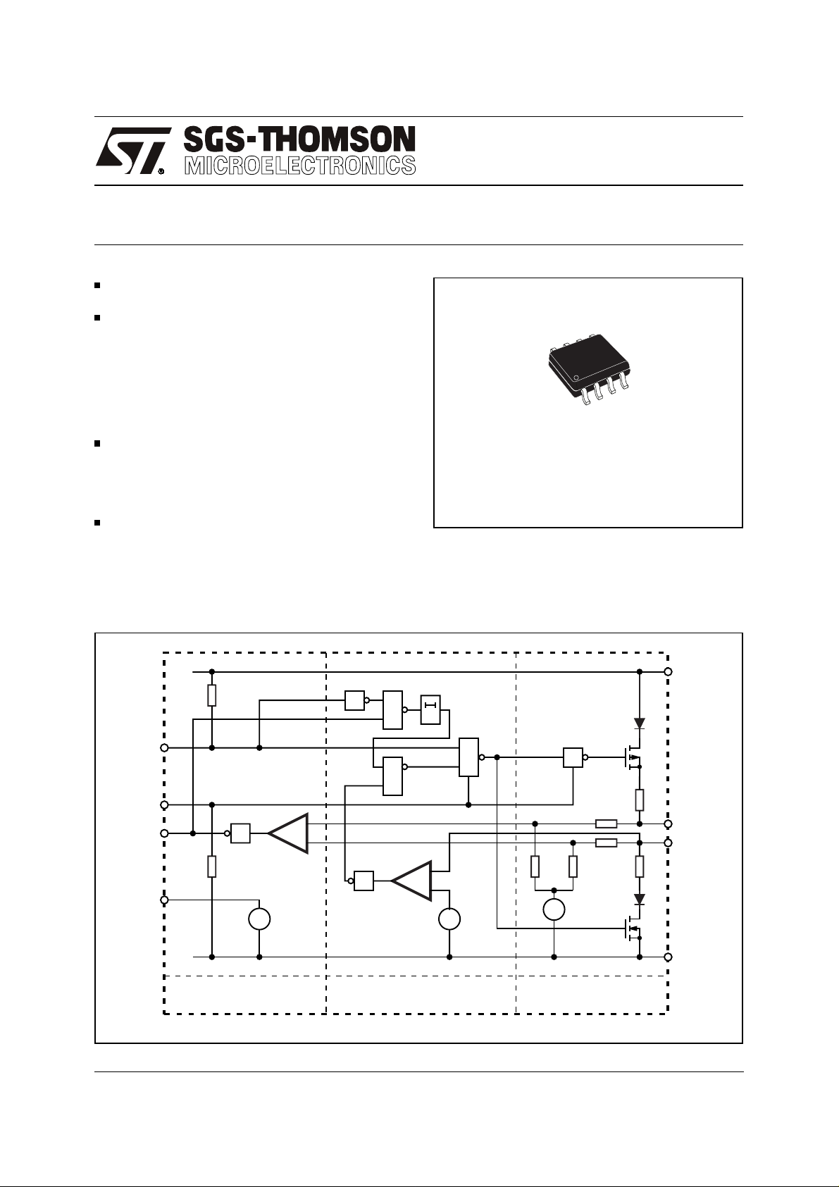
The L9615 is a bidirectional transceiver for signal
L9615
CAN BUS TRANSCEIVER
SO8
ORDERING NUMBER:
conditioning and processing in connection with a
CAN controller. Data rates of up to 500KBAUD
are supported using either shielded or nonshielded pair of lines.
L9615D
BLOCK DIAGRAM
1
TX0
8
ASC
4
RX0
5
RX1
1
&
td
1 V
V
REF
≥1
&
+
S
-
V
CLmax
+
-
MM
1
1
M
RECEIVER PROTECTION TRANSMITTER
3
7
6
2
D96AT245
V
S
C_H
C_L
GND
February 1998
1/8
Page 2
L9615
ABSOLUTE MAXIMUM RATINGS
Symbol Parameter Value Unit
V
S
, V
V
C_H
I
, I
C_H
C_L
V
DC
I
RXO
T
, T
stg
T
op
All voltages, except bus voltage, are defined with respect to pin 2
Positive currents flow into the IC.
PIN CONNECTION
Supply Voltage -0.3 to 7 V
Bus Voltage at C_H, C_L (VS 0 to 5.5V) -5 to 36 V
C_L
Off State Leakage Current at C_H, C_L ( VS =0 to 5.5V,
V
= -5 to 36V, V
C_H
= -5 to 36 )
C_L
-3 to 5 mA
DC Voltage at TXO, ASC (VS 0 to 5.5V) GND -0.3 to VS +0.3 V
Output Current at RXO (VS 0 to 5.5V) -0.3 to 1 mA
Storage and Junction Temperature Range -40 to 150 °C
J
Operating Temperature Range -40 to 110 °C
TX0
GND
V
S
RX0 RX1
2
3
4
D96AT246
8
7
6
5
ASC1
C_H
C_L
THERMAL DATA
Symbol Parameter Value Unit
PIN FUNCTIONS
N. Name Function
1 TXO Transmitter Input
2 GND Ground
3V
S
4 RXO Receive Output
5 RX1 Reference Voltage
6 C_L Low Side Bus Output
7 C_H High Side Bus Output
8 ASC Adjustable Slope Control
Supply Voltage
2/8
Page 3
L9615
ELECTRICAL CHARACTERISTICS
S
cessive: VTXO = V
; All voltages, except bus voltage, are defined with respect to pin 2. Positive currents
= -40 to 110°C; VS = 4.5 to 5.5V; Dominat: VTXO = GND; Re-
(T
OP
flow into the IC unless otherwise specified.)
Symbol Parameter Test Condition Min. Typ. Max. Unit
V
S
I
S
TRANSMITTER SECTION
C
TXO
V
TXO
I
TXO
C
ASC
V
ASC
I
ASC
, V
V
C_H
I
, I
C_H
R
IN(C_H, C_L)
R
Diff(C_H, C_L)
V
Diff
V
- V
C_H
V
Diff
V
- V
C_H
t
d
I
A
V
C_Lmax
Supply Voltage 4.5 5 5.5 V
Supply Current Dominant 80 mA
Recessive 20 mA
A
= 60Ω between C_H and C_L)
(R
TXO Input Capacitance 0V < V
TXO High Level Input Voltage 0.7 V
TXO
< V
S
25 pF
S
TXO Low Level Input Voltage 0 0.3 V
TXO High Level Input Current V
TXO Low Level Input Current V
ASC Input Capacitance 0V < V
ASC Input Voltage for High
= V
TXO
S
= GND -275 0 -25 µA
TXO
< V
ASC
S
-2 0 2 µA
25 pF
0 0.1 V
Speed
ASC Input Voltage for Low Speed 0.9 V
ASC Input Current V
Bus Voltage Recessive Recessive 0.4 VS0.5 Vs 0.6 Vs
C_L
Leakage Current Recessive VC_L = V
C_L
= V
ASC
S
V
= 0V -2 0 2 µA
ASC
= -2 to 7V -0.7 0.7 mA
C_H
= V
V
C_L
= 1 to 4V -0.3 0.3 mA
C_H
S
25 275 µA
Input Resistence Recessive 5 50 KΩ
Differential Input Resistence Recessive 10 100 KΩ
=
Differential Output Voltage Dominant, R
C_L)
=
Differential Output Voltage Recessive -500 0 50 mV
C_L)
Short Circuit Detection Time
RCS < 1Ω 1510µs
A
1.5 3 V
C_H to C_L ; C_H to B
Supply Current in Case of Short
150 mA
Circuit, C_H to C_L, C_H to B
(time = t
Overvoltage Protection
)
d
7810V
Threshold on C_L
V
VS
S
S
S
RECEIVE SECTION
V
V
V
C_H -VC_L
V
COM
+V
V
RXO
=
S
= (V
C_L
HYS
RXO High Level Output Voltage V
RXO Low Level Output Voltage V
Input Signal Threshold V
Input Common Mode Voltage
C_H
)/2
Range
Differential Input Hysteresis 150 mV
REFERENCE OUTPUT
V
RX1
R
RX1
Reference Voltage I
Output Resistance 2 9 KΩ
< 0.5V; I
Diff
V
= -2 to 7V; V
C_H
> 0.9V; I
Diff
V
= -2 to 7V; V
C_H
= -2 to 7V; V
C_H
= 0.3mA;
RXO
= 1mA;
RXO
0.9 V
= -2 to 7V;
C_L
= -2 to 7V;
C_L
= -2 to 7V; 500 700 900 mV
C_L
S
-2 7 V
= 0 0.45 VS0.5 VS0.55 V
RX1
Vs V
0.5 V
S
V
3/8
Page 4

L9615
DINAMIC CHARACTERISTICS
C
= 20pF between RXO and B; RA = 60Ω between C_H and C_L)
RXO
= 47pF between C_H and C_L; VS = 5V; tR < 5ns;
(C
A
Symbol Parameter Test Condition Min. Typ. Max. Unit
t
OT
S
R
t
OR
t
OTR
FUNCTIONAL DESCRIPTION
The L9615 is used as an interface between a
CAN controller and the physical bus. The device
provides transmitting capability to the CAN controller.
The transmitter outputs C_H and C_L are protected against short circuits and electrical transients which may occur in an automotive environment. In case of short circuit (C_H to C_L, C_H to
Signal Delay TXO to C_H, C_L 50 ns
Differential Output Slew Rate
(Transmitter)
Signal Delay C_H, C_L to R
Signal Delay TXO to R
XO
XO
V
= 0V 20 50 V/µs
ASC
V
= V
ASC
S
V
= 0V 150 ns
ASC
V
= 0V 300 ns
ASC
520V/µs
modes of operation: High speed (≤500kBaud) and
low speed (≤125kBaud).
The ASC pin is tied to GND for normal operation
at ≤500kBaud. For slower speed operation at
≤
125kBaud the rise and fall slope of the bus output can be decreased to r educe EMI by connectingg the ASC pin to V
S
.
FUNCTIONAL TABLE
B) the protection circuit recognizes this fault conditionand the transmitter output stages are disabled with a delay of max. 10µs to prevent destruction of the IC and high consumption of
C_L
supply current I
. If V
S
>V
C_Lmax
the transmitter
output stages would be disabled immediately.
TXO C_H C_L Bus State RXO
L H L Dominant L
H or
Floating
Floating
/2
V
S
Floating
VS/2
Recessive H
Pin ASC makes it possible to select two different
TYPICAL APPLICATION
V
Sn
CONTROLLER L9615 L9615 CONTROLLER
V
GNDn
V
GNDD
V
GNDm
4/8
SYSTEM n
R
R
A
A
CAN BUS
C_H
C_L
V
Sm
SYSTEM m
V
GNDm
V
Diff
D96AT247A
V
COM
Page 5

TIMING DIAGRAM
L9615
V
TX0
V
Diff
V
RX0
D96AT248
EMC PERF ORMANCE (R E C EI V ER )
CAN
CONTROLLER
1
MONITORING
(BIT COMPARISON)
CAN
CONTROLLER
2
t
R
t
OT
250Kbit/sec
250Kbit/sec
t
OTR
0.9V
t
OR
TRANSCELVER
TRANSCELVER
CAN
CAN
t
R
t
OT
0.5V
t
OR
t
OTR
EQUIVALENT TERMINATING
RESISTOR 2 x 120Ω
PARALLEL AT LINE ENDS
30Ω
1
2
30Ω
6.8∝F
450Ω
100Ω
6.8∝F
50Ω
Ust (Noise signal)
40dB
HP8640
90%AM, 1KHz
30V
20V
10V
U
ST
(V)
SS
SS
SS
NOT NOISE RESISTANT
L9615
NOISE RESISTANT
min. request boundary
(automotive industry)
10MHz1MHz 100MHz 500MHz 1GHz
D96AT249B
5/8
Page 6

L9615
EMC PERFORMANCE (TRANSMITTER)
4.7nF
TX0
50Ω
+5V
80dBµF
GND
V
S
Transceiver Without Emc Reducing Measures
80
70
60
ATTENUATION OF
TRANSMITTER
50
40
30
20
10
0
0 40 80 120 160 f(KHz)
D96AT251
10000
3162
1000
316.2
100
31.62
10
3.162
1
equivalent terminating resistor
2 x 120Ω parallel at line ends
C_H
C_L
30Ω
30Ω
4.7nF
50Ω
µV TEK495
Analyzer
D96AT250
Transceiver With Emc Reducing Measures
80
70
60
ATTENUATION OF
TRANSMITTER
50
40
30
20
10
0
0 40 80 120 160 f(KHz)
D96AT252
10000
3162
1000
316.2
100
31.62
10
3.162
1
EMC PERFORMANCE (Transceiver Sending)
TX0
50Ω
+5V
V
S
5V
250KHz
GND
Transceiver Without Emc Reducing Measures
80
70
60
50
40
30
20
10
D96AT254
10000
3162
1000
316.2
100
31.62
10
3.162
equivalent terminating resistor
2 x 120Ω parallel at line ends
C_H
C_L
30Ω
30Ω
4.7nF
50Ω
µV TEK495
Analyzer
D96AT253
Transceiver With Emc Reducing Measures
80
70
60
50
40
30
20
10
D96AT255
10000
3162
1000
316.2
100
31.62
10
3.162
6/8
0
0 40 80 120 160 f(KHz)
1
0
1
0 40 80 120 160 f(KHz)
Page 7

SO8 PACKAGE MECHANICAL DATA
L9615
DIM.
MIN. TYP. MAX. MIN. TYP. MAX.
A 1.75 0.069
a1 0.1 0.25 0.004 0.010
a2 1.65 0.065
a3 0.65 0.85 0.026 0.033
b 0.35 0.48 0.014 0.019
b1 0.19 0.25 0.007 0.010
C 0.25 0.5 0.010 0.020
c1 45° (typ.)
D 4.8 5.0 0.189 0.197
E 5.8 6.2 0.228 0.244
e 1.27 0.050
e3 3.81 0.150
F 3.8 4.0 0.15 0.157
L 0.4 1.27 0.016 0.050
M 0.6 0.024
mm inch
S8° (max.)
7/8
Page 8

L9615
Information furnishe d is believed to be acc urate and reliabl e. Howev er, SGS-THOM SON Mi croelect ronics as sumes no res pons ibility for the
consequences of us e of such information nor for any infringem ent of patents or other ri ght s of third parties which may result from its use. No
license is granted by impli cat i on or otherwise under any patent or patent rights of SGS-THOM SON Microelectronics. Specific ation me ntioned
in this publication are subje ct to change without notice. This publica tion supersedes and replaces all informa tion previously supplied. S GSTHOMSON Mic roelectronics products are not author ized for use as cri tical components in l ife support devices or systems with out express
written approval of SGS-THOMSON Micr oel ect roni cs.
© 1998 SGS-THOMSON Microelectronics – Printed in Italy – All Rights Reserved
SGS-THOMSON Microelectronics GROUP OF COMPANIES
Australia - Brazil - Canada - China - France - Germany - taly - Japan - Korea - Malaysia - Malta - Morocco - The Netherlands -
Singapore - Spain - Sweden - Switzerland - Taiwan - Thailand - United Kingdom - U.S.A.
8/8
 Loading...