

Page 1
OPERATING POWER SUPPLY VOLTAGE
RANGE 4.8V ≤
VS≤ 36V (40V FOR TRAN-
SIENTS)
REVERSE SUPPLY (BATTERY) PRO-
TECTED DOWNTOV
≥ -24V
S
STANDBYMODE WITHVERYLOWCURRENT
CONSUMPTIONIS
≤ 1µA@VCC≤0.5V
SB
MIN POSSIBLE BAUD RATE ACCORDING
TO ISO9141 ≥ 130KBAUD
TTL COMPATIBLETX INPUT
BIDIRECTIONAL K-I/O PIN WITH SUPPLY
VOLTAGEDEPENDENTINPUTTHRESHOLD
OVERTEMPERATURE SHUT DOWN FUNC-
TION SELECTIVETO K-I/O PIN
WIDE INPUT AND OUTPUT VOLTAGE
RANGE -24V≤ VK ≤ VS
KOUTPUTCURRENT LIMITATION,TYPIK= 60mA
DEFINEDOFF OUTPUT STATUS IN UNDER-
VOLTAGE CONDITION AND VS OR GND INTERRUPTION
CONTROLLEDOUTPUTSLOPEFORLOWEMI
HIGH INPUT IMPEDANCE FOR OPEN VS
OR GND CONNECTION
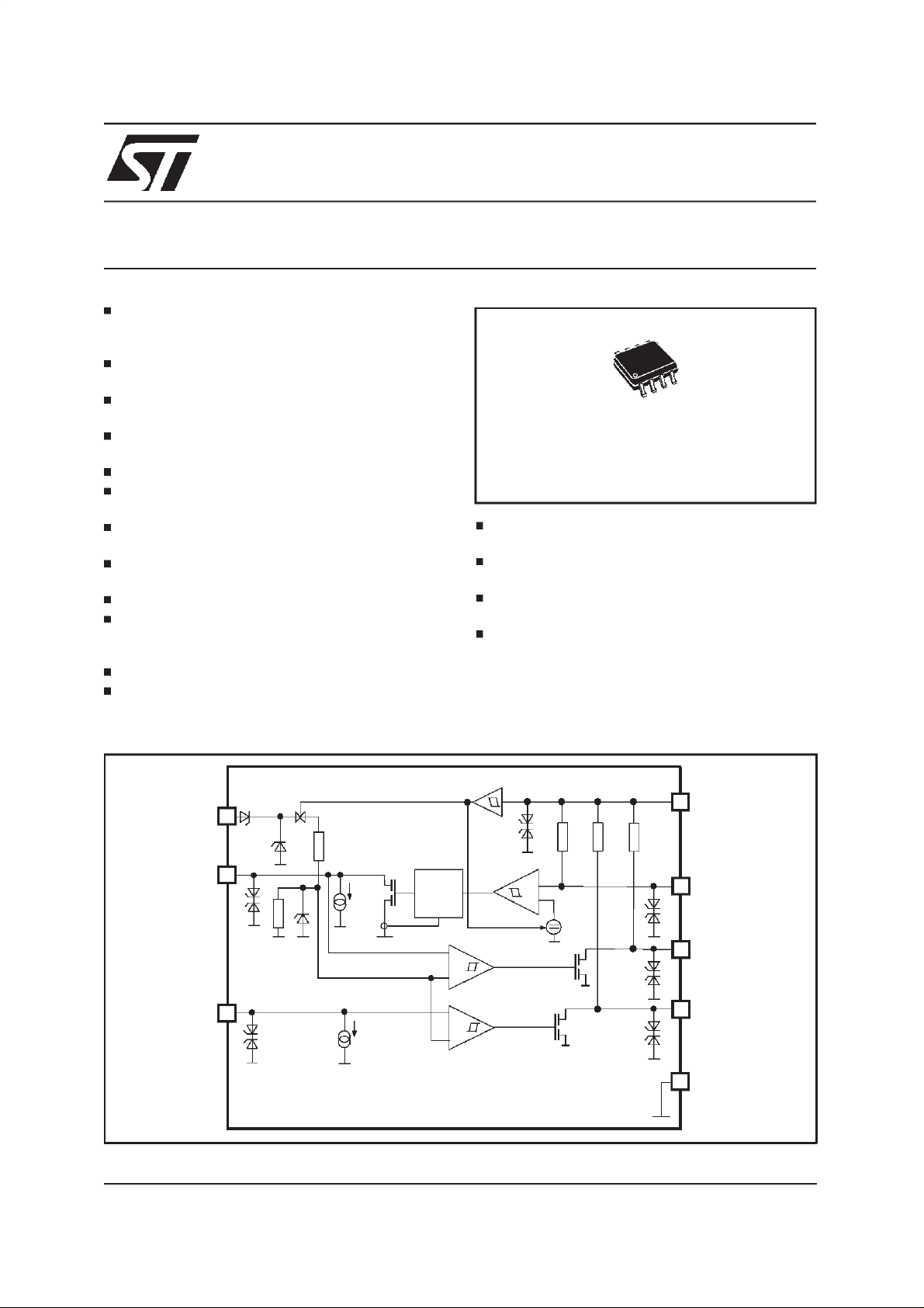
BLOCK DIAGRAM
L9613B
DATA INTERFACE
SO8
ORDERING NUMBERS: L9613B013TR (TAPE&REEL)
L9613B (TUBES)
DEFINED OUTPUT ON STATUS OF LO OR
RX FOR OPEN LI OR K INPUTS
DEFINED K OUTPUT OFF FOR TX INPUT
OPEN
INTEGRATED PULL UP RESISTORS FOR
TX, RX AND LO
EMI ROBUSTNESSOPTIMIZED
DESCRIPTION
The L9613B is a monolithicintegrated circuit containing medium speed data interface functions.
November 1999
VS
LI
RTX
K
IK
OFF
IK
T
jMON
SC
+
-
RLO
1,75V
RRX
TX
RX
+
VCC
-
ILI
+
LO
GND
1/10
Page 2
L9613B
ABSOLUTE MAXIMUM RATINGS
Symbol Parameter Value Unit
V
S
Supply Voltage
ISO transient t ≤ 400ms
V
CC
/dt Supply Voltage Transient -10 to +10 V/µs
dV
S
V
LI,K
V
LO, RX, TX
* max ESD voltages are +/-2KV with human body model C=100pF, R=1.5KΩ corresponds to maximum energy
Stabilized Voltage -24V to 7 V
Pin voltage -24 to V
Pin voltage -24 to V
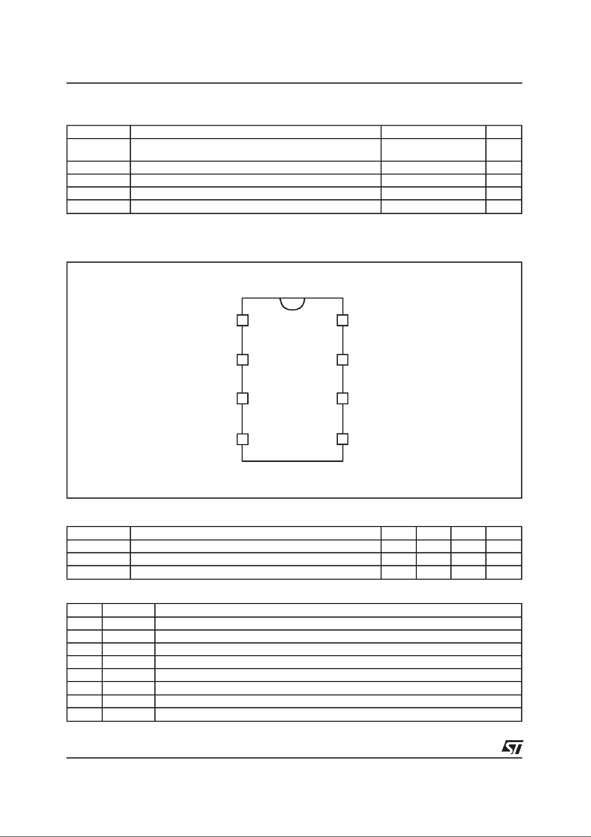
PIN CONNECTION
-24 to +36
-24 to +40
S
CC
V
V
V
V
RX
LO
VCC
TX
1
2
3
4
8
7
6
5
LI
VS
K
GND
THERMAL DATA
Symbol Parameter Min. Typ. Max. Unit
T
T
R
JSDon
JSDoff
th(j-a)
Temperature shutdown switch-on-threshold 160 200 °C
Temperature shutdown switch-off-threshold 150 °C
Thermal steady state junction to ambient resistance 130 155 180 °C/W
PIN FUNCTIONS
N. Name Description
1 RX Output for K as input
2 LO Output L comparator
3 VCC Stabilized voltage supply
4 TX Input for K as output
5 GND Common GND
6 K Bidirectional I/O
7 VS Supply voltage
8 LI Input L comparator
2/10
Page 3
L9613B
ELECTRICAL CHARACTERISTICS (The electrical characteristics are valid within the below defined
OperatingConditions, unless otherwise specified).
The function is guaranteedby design until T
V
S
V
CC
T
J
Symbol Parameter Test Condition Min. Typ. Max. Unit
VTX
Note 1) For external supplied output currentslower than this value a series protection diode can become active. See also Fig. 4 and 5.
Supplyvoltage 4.8 V... 18 V
Stabilizedvoltage 3 V... 7 V
Junctiontemperature -40 °C... 150°C
I
CC
IS
ON
IS
SB
VK
low
VK
high
VK
hys
IK
OFF
RK
ON
IK
SC
VK
sat
VTX
RRX
RLO
VRX
VLO
IRX
ILO
RTX Input pull up resistance Output status = (HIGH)
RTX Input pull up resistance -0.15V≤VTX≤VCC + 0.15V
VLI
low
VLI
high
ILI Input current VS, VCC ≥ 0V or
Supply VCCCurrent V
Supply VS Current VLI,VTX = 0V 3.5 10 mA
Input Voltage LOW State RX output status LOW -24 0.40VS V
Input Voltage HIGH State RX output status HIGH 0.60VS VS V
Input Threshold Hysteresis VK
Input Current VTX ≥ VTX
Output ON Impedance @ V
Short Circuit Current VS≥ 6.5V 40 60 150 mA
Output Saturation Voltage RKO= 1.5K
Input Voltage
low
LOW State -24 1 V
Input Voltage
high
HIGH State 3.5 VCC V
Output ON Impedance VK ≤ VK
ON
ON
Saturation Output Voltage No external load 1 V
sat
sat
Output short circuit current VS≥ 6.5V
SC
SC
Input voltage LOW state LO output status LOW -24 0.40VS V
Input voltage HIGH state LO output status HIGH 0.60VS VS V
temperatureshutdownswitch-on-threshold.
JSDon
5.5V
≤
CC
VLI, VTX = 0V
VK≥VK
VLI≥VLI
VTX = V
high
high
CC
-5 40 150
@VCC≤ 5.5V
= 0.5V
V
CC
@V
12V 3)
≤
S
VCC= 0.5V, see fig. 5
@V
≤16V
S
-VK
high
V
S
V
≥ 6.0V
S
VS,V
V
CC
VTX ≤ VTX
low
8.0V
≥
high
CC
0V or V
≥
,
S
= open or GND = open
6.5V
≥
S
IK ≥ 7mA 1)
low
0.2
0.08
-5 4 40 µA
Ω
; VLI ≤ VLI
low
6.5V; I
V
≥
S
RX,LO
≥
low
1mA
92050mA
51018k
T
85°C
≤
A
-0.15V ≤ VLO ≤ VCC + 0.15V
-0.15V≤VRX≤VCC + 0.15V
10 20 40 k
T
125°C
≤
amb
-5 4 40 µA
VS, VCC = open or
GND = open
1.4 2.5 mA
µ
<1 50
100
µ
µ
0.05VS 1.0 V
10 30
1V
40 90 Ω
A
A
A
V
Ω
Ω
Ω
3/10
Page 4

L9613B
ELECTRICALCHARACTERISTICS(continued)
Symbol Parameter Test Condition Min. Typ. Max. Unit
C
KI,LO,RX
f
LI-LO
f
K-RX
f
TX-K
f
LI-LO
f
K-RX
f
TX-K
t
OFF,LI-LO
t
OFF,K-RX
t
OFF,TX-K
t
ON,LI-LO
t
ON,K-RX
t
ON,TX-K
td
SB ON
td
SB OFF
Note 2) Speed limitationrelated to external capacitance C
Note 3) In case of spikes on VCC≥0.5V KOUT will be switched On for typical 10µs whichrepresents the standby td
Internal output capacities 20 pF
Transmission frequency 9V < VS< 16V,
130 kHz
(external loads)
T
min
Rise Time for the definitionof tr, tf see
≥20⋅
R
C
⋅
KO
K-Kline
0.4 2 µs
FIG. 1, 2)
Fall Time 9V < V
< 16V,
S
0.4 2
(external loads)
T
min
Switch OFF time for the definitionof tr, tf see
≥20⋅
R
C
⋅
KO
K-Kline
1.3 3
FIG. 1
Switch ON time 9V < VS< 16V,
1.3 3 µs
(external loads)
Tmin≥20⋅R
Standby reaction time VTX = 0V, IK≥7mA
KO
C
⋅
K-Kline
10
20
VLI = 0V, 9V < VS < 16V
t
r=RLO,RX
see FIG. 2
andinternal impedance C
extRX, LO
⋅(C
LO,RX+CextRX,LO
)⋅ 1.38.
, RLO,RRX for rise time.
LO,RX
20
SB
40
reaction time.
s
µ
s
µ
s
µ
s
µ
FUNCTIONAL DESCRIPTION
The L9613B is a monolithic bus driver designedto provide bidirectional serial communication in automotive applications.
The device provides a bidirectional link, called K, to the V
separate comparator L which is also able to be linked to the V
related diagnosis bus. It also includes a
Bat
bus. The input TX and output RX of K
Bat
are related to VCC with her integrated pull up resistances. Also the L comparator output LO has a pull
up resistanceconnectedto VCC.
All VBat bus defined inputs LI and K have supply voltage dependent thresholds together with sufficent
hysteresis to suppress line spikes. These pins are protected against overvoltages, shorts to GND and
VS and can also be driven beyond VS and GND. These features are also given for TX, RX and LI only
taking into account the behaviour of the internal pull up resistances. The thermal shut down function
switches OFF the K output if the chip temperatureincreases above the thermalshut down threshold. To
reactivate K again the chip temperaturemust decrease below the K switch ON temp. To achieve no fault
for VS undervoltage conditions the outputs will be switched OFF and stay at high impedance. The device is also protected against reverse battery condition. During lack of VS or GND all pins shows high
impedance characteristic. To realize a lack of the VS related bus line LI and K the outputs LO and RX
shows defined ON status. Supressing all 4 classes of ”Schaffner” signals (Schaffner 1; 2; 3a,b; 4) all
pins can be load with short energy pulses of max. ±0.2mJ. All these features together with a high possible baud rate >130Kbaud, controlled output slopes for low EMI, a wide power supply voltage range and
a real standby function with zero power consumption IS
≤ 1µA during system depowering VCC
SB typ
≤0.5V makethis devicehigh efficient for automotivebus system.
After wake up of the system from SB condition the first output signal will have an additional delay time
td
≤ 5µs.
typ
The typical output voltage behaviour for the K, LO, RX outputs as a function of the output current is
shown in Fig.5. Fig.6 shows a waveform of the output signal when the low level changes from R
to I
⋅ 2 ⋅ RON+UBEstate. This variation occurs due to too low output current or after a negative tran-
OUT
ON
⋅ I
OUT
sient forced to the output or to the supplyvoltage line.
4/10
Page 5

Figure 1. Input to output timings and output pulse shape
V
IN
V
OUT
80% 80%
L9613B
t
20%
t
OFF
Figure 2. Standby reaction time.
5V
VCC
0V
80%
VK
20%
td
SB
ON
VLO
VCC
80%
20%
t
r
td
SB
OFF
t
f
t
ON
t
td
SB
ON
5/10
Page 6

L9613B
Figure 3. Output characteristicsat K, LO, RX.
I
OUT
I
OUT
MIN
N
O
S
D
R
V
OUT
I
=
R
OUT DSON
*
protection diode
V
Figure 4. Output signal shape relatedto outputcurrent.
V
IN
V
OUT
I
OUT
R+U
2
* * DSON
OUT
*
RI
DSON
BE
I
OUT
I
>
OUT
MIN
OUT
′<I
I
OUT
I
=
OUT DSON
OUT
1
MIN
2
**
I
OUT
+U
R
BE
V
OUT
t
>
I
OUT
MIN
t
6/10
Page 7

Figure 5. Standby current consumption.
IS
SB
100µA
50µA
L9613B
Ω
k
0
≈ 5
R
Figure 6. ApplicationCircuit.
VS
510
0.4Ω
Ω
Diagnostic
Tester
K
L
KLine
40V
R
KO
12V 16V
VS
IK
K
C
K
IK
SC
T
jMON
OFF
RTX RLO RRX
+
1,75V
-
LI
ILI
+
-
+
VS
VCC
TX
RX
LO
GND
I/O
I/O
I/O
5V
VCC
uP
VDD
ECU1
LLine
K
C
K
LI
ECU2
7/10
Page 8

L9613B
EMS Performance(ISO 9141 BUS system)
Figure 7.
VS= 12V
=
510
Ω
∆
Signalcomparison
Figure 8.
50
10kHz
∆≤ ± 10%
P
i(mW)
10000
Ω
5000
VS
TX K
U713
VS
RX
U713
K
not incidentpower resistant
1.5nF
136
Ω
68Ω
Probe
NAP - 73
P
i
NAP
40dB
P
=5W
imax
Rhode& Schwartz
SMG
0.1 - 1000MHz
1000
100
1 10 100 1000
incident power resistant
ESD applicationhints
To improve the ESD robustness of this device
above specified ±2KV/HBM external blocking capacitors must be used. Neverthelessthe max. energy which can be clamped by this device should
not exceeds0.2mJ for each pin. An equivalent input diagramfor calculation can be seen in fig. 9.
ESD duschargemodel
E
8/10
ESD
1
=
2
C
HBMUESD
2
= 0.2mJ +
1
C
EXT
2
⋅ (45V)
2
Figure 9.
C
HBM
100pF
R
1.5k
HBM
f
(MHz)
Ω
C
ext
45V
45V
≤ 0.2mJ
E
Page 9

L9613B
DIM.
D (1) 4.8 5.0 0.189 0.197
F (1) 3.8 4.0 0.15 0.157
(1) D and F do not include mold flash or protrusions.Mold flash or
MIN. TYP. MAX. MIN. TYP. MAX.
A 1.75 0.069
a1 0.1 0.25 0.004 0.010
a2 1.65
a3 0.65 0.85 0.026 0.033
b 0.35 0.48 0.014 0.019
b1 0.19 0.25 0.007 0.010
C 0.25 0.5 0.010 0.020
c1 45° (typ.)
E 5.8 6.2 0.228 0.244
e 1.27 0.050
e3 3.81 0.150
L 0.4 1.27 0.016 0.050
M 0.6 0.024
S8°(max.)
potrusions shall not exceed 0.15mm (.006inch).
mm inch
0.065
OUTLINE AND
MECHANICAL DATA
SO8
9/10
Page 10

L9613B
Information furnished is believed to be accurate and reliable. However, STMicroelectronics assumes no responsibility for the consequences
of use of such information nor for any infringement of patents or other rights of third parties which may result from its use. No license is
granted by implication or otherwise under any patent or patent rights of STMicroelectronics. Specification mentioned in this publication are
subject to change without notice. This publication supersedes and replaces all information previously supplied. STMicroelectronics products
are not authorized for use as critical components in life support devices or systems without express written approval of STMicroelectronics.
The STlogo is a registered trademark of STMicroelectronics
1999 STMicroelectronics – Printedin Italy – All Rights Reserved
STMicroelectronics GROUP OF COMPANIES
Australia - Brazil - China- Finland - France - Germany - Hong Kong - India - Italy - Japan - Malaysia - Malta - Morocco -
Singapore - Spain - Sweden - Switzerland- United Kingdom - U.S.A.
10/10
 Loading...