

Page 1
L9386MD
DUAL INTELLIGENT POWER LOW SIDE SWITCH
DUAL POWER LOW SIDE DRIVER WITH 2 x
5A
LOW R
TYPICALLY200mΩ@TJ=25°C
DSON
INTERNAL OUTPUT CLAMPING DIODES
=50V FOR INDUCTIVE RECIRCULATION
V
FB
LIMITED OUTPUT VOLTAGE SLEW RATE
FOR LOW EMI
µP COMPATIBLEENABLE AND INPUT
WIDE OPERATING SUPPLY VOLTAGE
RANGE4.5V TO 45V
REAL TIMEDIAGNOSTIC FUNCTIONS
- OUTPUTSHORTED TO GND
- OUTPUTSHORTED TO VSS
- OPENLOAD
- LOADBYPASS
- OVERTEMPERATURE
DEVICEPROTECTIONFUNCTIONS
- OVERLOADDISABLE
- REVERSEBATTERY UP TO -16V @ V
- THERMALSHUTDOWN
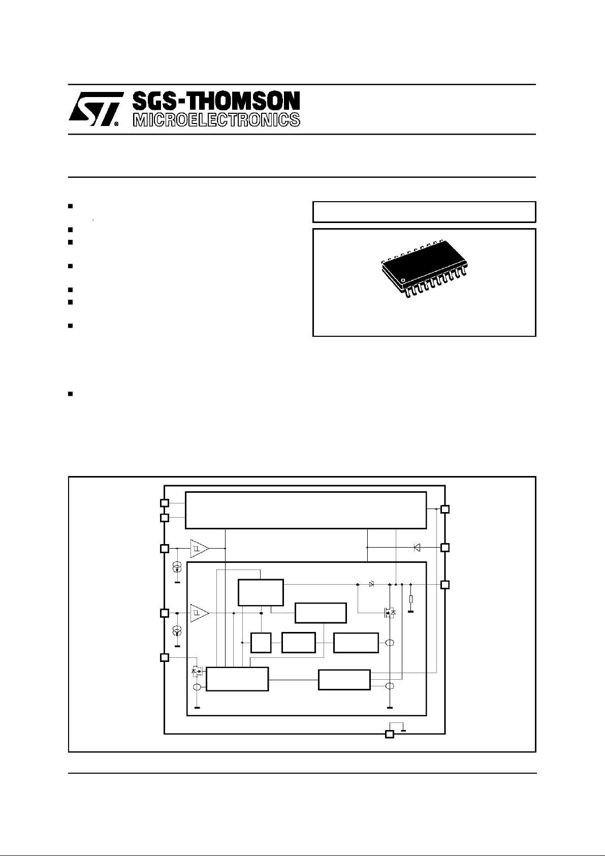
BLOCK DIAGRAM
IN1
DIAG1
S
Channel 1
MULTIPOWERBCD TECHNOLOGY
SO20 (12+4+4)
ORDERING NUMBER: L9386MD
DESCRIPTION
The L9386MD is a monolithic integrated dual low
side driver realized in an advanced MultipowerBCD mixed technology. It is especially intended
to drive valves in automotive environment. Its inputs are µP compatible for easy driving.Particular
care has been taken to protect the device
against failures, to avoid electro-magnetic interferences and to offer extensive real time diagnostic.
OUT1
VS
OUT2
DIAG2
IN2
EN
Diagnostic
Control
Output
Control
R
QS
Delay
Timer
Overtemp
Overload
Openload
R
O
Channel 2
GND
January 1995
This is advanced information on a new product now in development or undergoing evaluation. Details are subject to change without notice.
1/10
Page 2
L9386MD
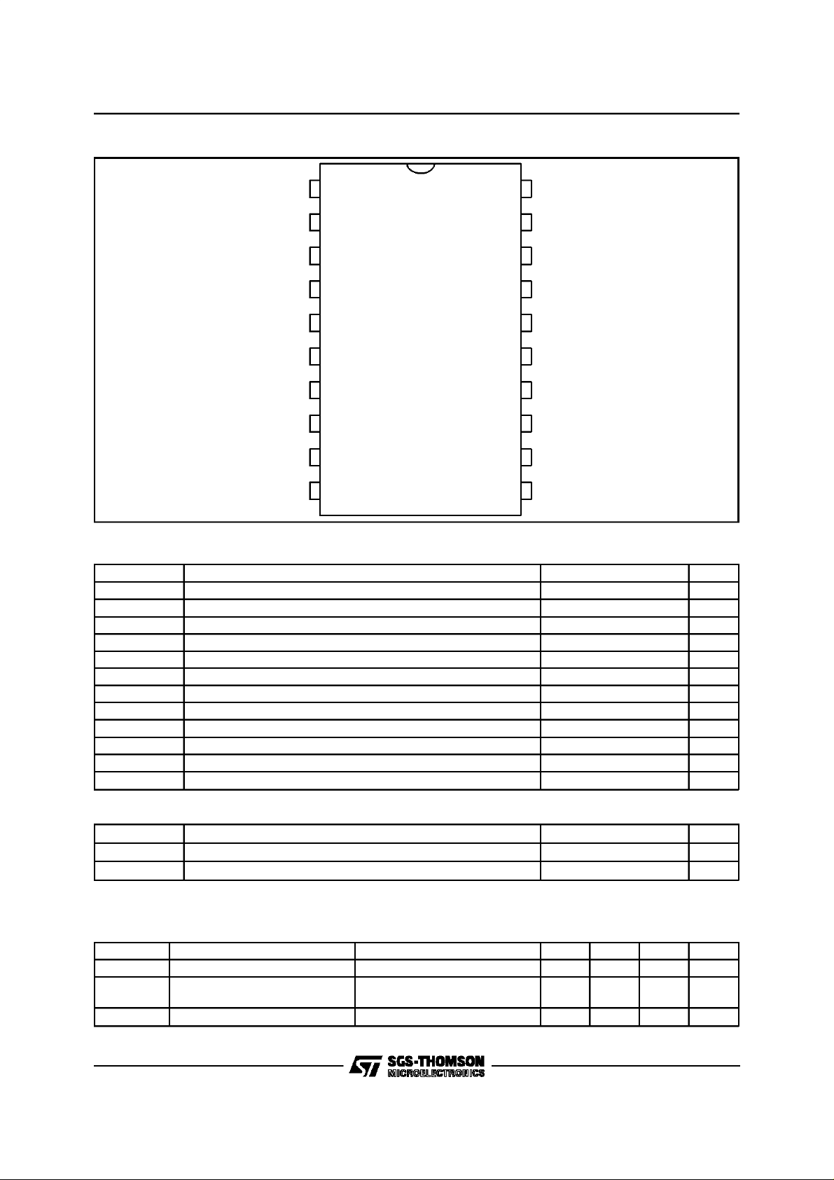
PIN CONNECTION(Top view)
IN1
DIAG2
OUT2
GND
GND
GND
GND
N.C.
EN
VS
ABSOLUTE MAXIMUM RATINGS
1
2
3
4
5
6
7
8
9
10
(no damage or latch)
IN2
20
DIAG1
19
OUT1
18
GND
17
GND
16
GND
15
GND
14
N.C.
13
N.C.
12
N.C.
11
Symbol Parameter Value Unit
VS
DC
VS
TR
V
IN,EN
VD
DC
VO
DC
VO
TR
I
O
I
OR
EO Switch-off energyfor inductive loads (t
T
jEO
T
j
T
a
DC supply voltage -16 to 45 V
Transient supply voltage ( t ≤ 500ms ) 60 V
Input voltage ( | ≤ | 10mA | ) -1.5 to 6 V
Diagnostic DC output voltage ( |≤| 50mA | ) -0.3 to 16 V
DC output voltage 45 V
Transient output voltage ( R
)60V
≥4Ω
L
Output load current internal limited
Reverse outputcurrent limited by load -4 A
= 250µs, T = 5ms) 50 mJ
EO
Junction temperature during switch-off ∑t = 30min 175 °C
Junction temperature -40 to +150 °C
Storage temperature -55 to +150 °C
THERMAL DATA
Symbol Parameter Value Unit
T
jDIS
R
th j-pins
ELECTRICAL CHARACTERISTICS
Thermal disable junction temperature threshold 160 to 190
Thermal resistance junction to pins 14
(Operating Range) - The electrical characteristics are valid within
the below defined operative range, unless otherwise specified.
Symbol Parameter Test Condition Min. Typ. Max. Unit
2/10
V
S
V
D
T
j
Board supply voltage 4.5 12 32 V
Stabilized diagnostic output
-0.3 5 16 V
voltage
Junction Temperature -40 150 °C
°
C/W
°
C
Page 3
L9386MD
ELECTRICALCHARACTERISTICS
(continued)
Symbol Parameter Test Condition
IS
SB
Static standby supply current b)
c) V
EN
=L,VO≤VO
IS DC supply current b)
VD
ID
LE
Diagnostic ouput low voltage b) ID= 2mA
L
Diagnostic output leakage
current
ID Diagnostic output current
c) V
EN=VIN
c) I
D
VS = 0V or VS = open;
VD = 5.5V T
VD ≤ 16V DIAG = L 2 6 30 mA
= 1mA
=H
≤
j
capability
VO
UV
VO
∆
UV1,2
Open load voltage threshold VEN=X,VIN= L 0.51
Open load difference voltage
threshold
b) VEN = X, V
VS ≥ VO
C
≥ VO
IN1,2
VOC= output voltage of other
channel
c)
IO
UC
Open load current threshold a) VEN=VIN=H
c)
IO
VO
S
ON,OFF
R
R
DSON
V
(EN,IN)L
OC
IO
Over load current threshold b) 5 7 A
Output voltage during clamping IO
CL
100mA 45 52 60 V
≥
CL
Output (fall, rise) slew rate a) Fig. 2 200 1500 3200 V/ms
Internal output pull down resistor VEN= L 10 20 40 KΩ
Output on resistance VS > 9.5V IO = 2A
T
=25°C
j
T
= 150°C
j
Logic input low voltage |I
EN, IN
|≤10mA
b)
c)
V
(EN,IN)H
V
(EN,IN)hys
I
EN
I
IN
t
DON
t
D OFF
t
D H-L, Diag.
t
D IOu
t
DOL
Logic input high voltage 2.2 5.5 V
Logic input hysteresis 0.2 0.4 1 V
Enable input sink current 1V≤V
Logic input sink current 1V≤V
5.5V 10 30 60
≤
EN
5.5V 40 95 180
≤
IN
Output delay ON time a) Fig. 2 4 25
Output delay OFF time a) Fig. 2 5 15 30 µs
Diag. delay output OFF time a) Fig. 2 5 30 65 µs
Diagnostic open load delay time a) Fig. 4 8 50 µs
Diagnostic overload delay
a) Fig. 1 50 160 300 µs
switch-off time
125°C
=L
UV
Value
T
j1
Unit
Min. Typ. Max.
0.73 1.5
uv
15
1.3 5
15
mA
mA
mA
mA
0.35 0.5 V
0.1 2 µA
xVS
VO
0.9V
VO
0.7V
100
20
-1.5
-1.5
0.55
xVS
-
VO
C
1.25V
VO
-
C
1.25V
320 480 mA
200 300
0.59
V
xVS
-
VO
C
C
1)
-
V
1.6V
VO
-
C
C
V
-
1.8V
mA
mΩ
500
1
0.5
m
Ω
V
V
A
µ
A
µ
s
µ
a) 9V ≤ VS≤16V (Nominal operating range)
R
≤ 6Ω,
L
≤ IO
I
O
b) 6.5V ≤ VS≤ 16V(Diagnostic operation range)
c) 4.5V ≤ V
1) Limit under evaluation.
OC
< 6.5V and 16V < VS≤ 32V (Extended operation range)
S
3/10
Page 4

L9386MD
DIAGNOSTICTABLE
(Operatingrange: 4.5V≤V
≤
32V)
S
Conditions EN IN Out Diag.
Normal function L
GND short VO
Load bypass ∆VO
Open load IO
175°C
T
≥
j typ
< 0.55V L X off H
typ
≥ 1.25V H L off H
1,2
< 320mA H H on (*) L
typ
Oertemperature (**)
Latched Over load IO
> 5A X H off L
min
H
H
X
X
X
L
H
L
H
off
off
on (*)
off
off
L
L
H
H
L
Reset over load latch X D.C. D.C.
(*) for 4.5V ≤ VS < 6.5V, IO ≤ 2A diag. table is valid.
(**) Ifone diag.status showsthe overtemp.recognition,in parallel thisoutput will be switchedOFF internally.The correspondingchannelshould
be switched OFF additional by its Input or ENABLE signal, otherwise the overload latch will be set after t
be related to the overdrop sensing which will be used as over load recognition.
Figure 1:
Diagnosticoverload delay time
UI
5V
is passed. This behaviour will
DOL
t
IO
IO
SC
5A
IO
UC
td
OL
UD
5V
t
t
4/10
Page 5

L9386MD
Figure 2:
V
V
U
0.85VO
VS-VO
0.85VS
VO
0.15VS
Outputslope.
U
IN
5V
(IN)H
(IN)L
OUT
VO
C
C
VS
CC
UV
td
on
S
on
td
off
S
off
t
t
V
0.5V
DIAG
V
D
D
t
D
H-L
Diag
t
5/10
Page 6

L9386MD
Figure 3:
Blockdiagram - Open load voltage detection.
L1 L2
OUT1 OUT2
IN
1
VS
55%
R
IO
-
V
Batt.
IN
R
IO
+
+
-
2
Enable
&&
R
S
Latch
Latch
S
Q
R
Q
&&
VO
UV1
VO
UV2
6/10
Page 7

L9386MD
Figure 4:
Logic diagram.
open load
voltage
normal
operation
OFF
ON
open load voltage
open load current
latch reset
off
td
normal
operation
u
on
td
IO
td
latched over.
load diagnostic
OL
td
over load
current
open load
current
normal
operation
u
on
td
IO
td
open load current
normal
operation
OFF ON
EN
V
IN
V
u
VO
o
IO
u
IO
D
V
7/10
Page 8

L9386MD
CIRCUIT DESCRIPTION
The L9386MD is a dual low side driver for inductive loads like valves in automotive environment.
The device is enabled by a common CMOS compatible ENABLE high signal. The internal pull
down current sources at the ENABLE and INPUT
pins protect the device in open input conditions
against malfunctions. An output slope limitation
for du/dt is implementedto reduce the EMI. An integrated active flyback voltage limitation clamps
the output voltage during the flyback phase to
50V.
Each driver is protected against short circuit and
thermal overload. In short circuit condition the
output will be disabled after a short delay time
to suppress spikes. This disable is latched
t
DOL
until a negativeslope occure at the correspondent
input pin. The thermal disable for T
> 175°Cof
J
the output will be reseted if the junction temperature decreases about 20°C below the disable
thresholdtemperature.
For the real time error diagnosis the voltage and
the current of the outputs are compared with internal fixed values VO
conditions to recognizeopen load (R
for OFF and IOUCfor ON
UV
≥
20KΩ,R
L
>38Ω) in ON and OFF conditions. The diagnostic
Figure 5:
Applicationcircuit diagram.
operatesalso in the extendedsupply voltage rang
of 4.5V ≤ VS≤ 32V.
Also the output voltages VO
are compared
1,2
against each other in OFF condition with a fixed
offset of∆VO
to recognize GND bypasses.
UV 1,2
To suppress mail∆VO diagnoses during the flyback phases of the compared output, the ∆VO diagnostic includes a latch function. Reaching the
flyback clamping voltage VO
the diagnostic sig-
C
nal is reseted by a latch. To activate again this
kind of diagnostic a low signal at the correspondent INPUT or the ENABLE pin must occur (see
also Fig.3).
The diagnostic output level in connection with different ENABLE and INPUT conditions allows to
recognizedifferent fail states,like overtemp,short
to VSS, short to GND, bypass to GND and disconnected load (see also page 7 diagnostic table).
The diagnostic output is also protected against
short to UD
threshold IO
. Overstepingthe over load current
max
, the output current will be limited in-
o
ternally during the diagnostic overload delay
switch-offtime t
L
DOL
.
+5V
µ P
Controller
DIAG1
DIAG2
IN1
EN
IN2
Diagnostic
Control
Output
Control
R
QS
Channel 1
Delay
Timer
Channel 2
Overtemp
Overload
Openload
GND
Z
VALVE
OUT1
VS
OUT2
R
O
Z
VALVE
V
Batt
8/10
Page 9

SO20 PACKAGEMECHANICAL DATA
L9386MD
DIM.
MIN. TYP. MAX. MIN. TYP. MAX.
A 2.65 0.104
a1 0.1 0.3 0.004 0.012
a2 2.45 0.096
b 0.35 0.49 0.014 0.019
b1 0.23 0.32 0.009 0.013
C 0.5 0.020
c1 45 (typ.)
D 12.6 13.0 0.496 0.512
E 10 10.65 0.394 0.419
e 1.27 0.050
e3 11.43 0.450
F 7.4 7.6 0.291 0.299
L 0.5 1.27 0.020 0.050
M 0.75 0.030
S 8 (max.)
mm inch
9/10
Page 10

L9386MD
Information furnished is believed to be accurate and reliable. However, SGS-THOMSON Microelectronics assumes no responsibility for the
consequences of use of such information nor for any infringement of patents or other rights of third parties which may result from its use. No
license is granted by implication or otherwise under any patent or patentrights of SGS-THOMSON Microelectronics. Specification mentioned
in this publication are subject to change without notice. This publication supersedes and replaces all information previously supplied.
SGS-THOMSON Microelectronics products are notauthorized foruseas criticalcomponents in life support devicesor systemswithoutexpress
written approval of SGS-THOMSON Microelectronics.
1996 SGS-THOMSON Microelectronics – Printedin Italy – All Rights Reserved
SGS-THOMSON Microelectronics GROUP OF COMPANIES
Australia - Brazil - Canada- China - France - Germany - Hong Kong - Italy - Japan - Korea - Malaysia - Malta - Morocco - The Netherlands -
Singapore - Spain - Sweden - Switzerland- Taiwan - Thailand - United Kingdom - U.S.A.
10/10
 Loading...