

Page 1
®
L9377
DUAL INTELLIGENT POWE R LOW SIDE SWITCH
DUAL POWER LOW SIDE DRIVER WITH 2 x
5A
LOW R
TYPICALLY 200mΩ @ TJ = 25°C
DSON
INTERNAL OUTPUT CLAMPING DIODES
V
=50V FOR INDUCTIVE RECIRCULATION
FB
LIMITED OUTPUT VOLTAGE SLEW RATE
FOR LOW EMI
P COMPA TIBLE ENAB L E AND INPUT
µ
WIDE OPERATING SUPPLY VOLTAGE
RANGE 4.5V TO 45V
REAL TIME DIAGNOSTIC FUNCTIONS:
- OUTPUT SHORTED TO GND
- OUTPUT SHORTED TO VSS
- OPEN LO AD
- LOAD BYPA SS
DEVICE PROTECTION FUNCTIONS:
- OVERLO AD D I SA BL E
- REVERSE BATTERY UP TO -16V @ V
S
- THERMAL SH UTDOW N
DESCRIPTION
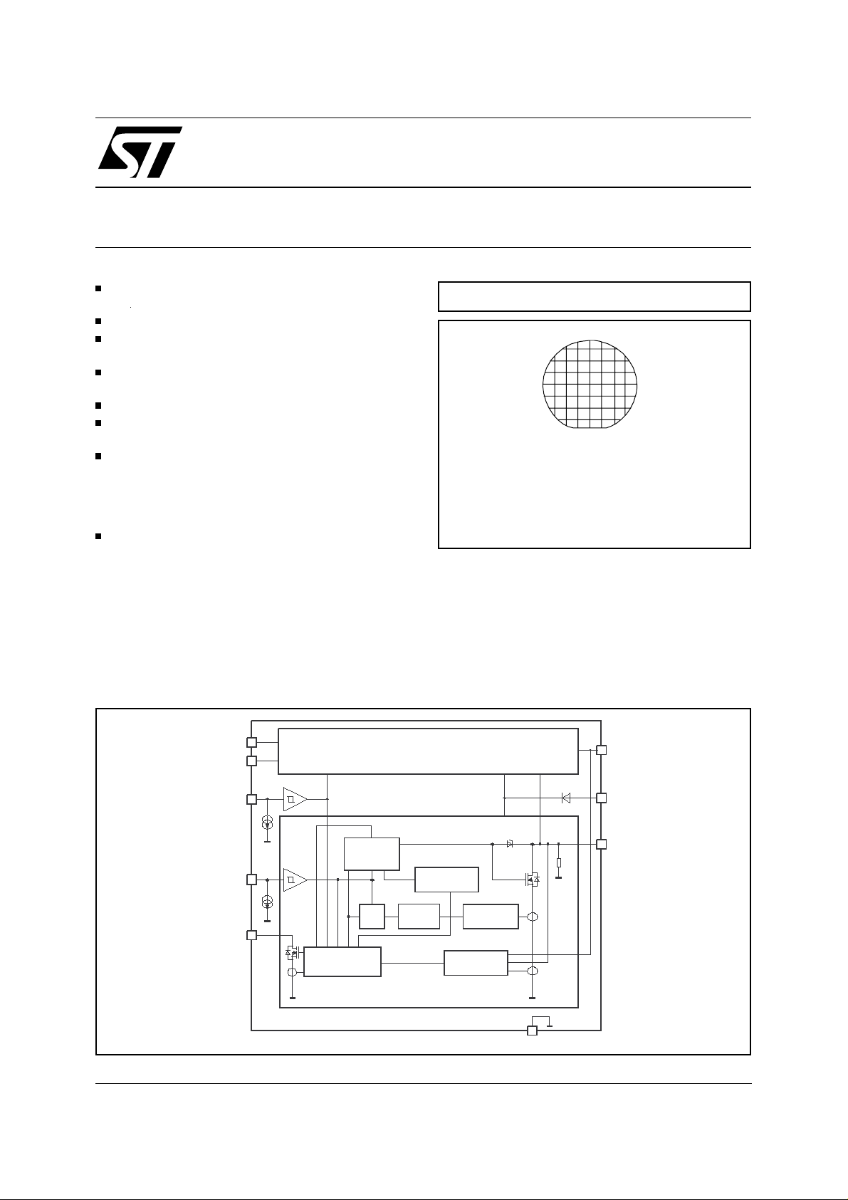
The L9377 is a monolithic integrated dual low
side driver realized in an advanced Multipower-
BLOCK DIAGRAM
MULTIPOWER BCD TECHNOLOGY
DIE
ORDERING NUMBER:
L9377DIE1
BCD mixed technology. It is especially intended
to drive valves in automotive environment. Its inputs are µP compatible for easy driving. Particular
care has been taken to protect the device
against failures, to avoid electro-magnetic interferences and to offer extensive real time diagnostic.
July 2000
IN1
DIAG1
EN
IN2
DIAG2
Diagnostic
Control
Output
Control
R
QS
Channel 2
Channel 1
Overtemp
Delay
Timer
Overload
Openload
GND
OUT1
VS
OUT2
R
O
1/9
Page 2
L9377
ABSOLUTE MAXIMUM RATINGS
(no damage or latch)
Symbol Parameter Value Unit
VS
DC
VS
TR
V
IN,EN
VD
DC
VO
DC
VO
TR
I
O
I
OR
DC supply voltage -16 to 45 V
Transient supply voltage ( t ≤ 500ms ) 60 V
Input voltage ( | ≤ | 10mA | ) -1.5 to 6 V
Diagnostic DC output voltage ( | ≤ | 50mA | ) -0.3 to 16 V
DC output voltage 45 V
Transient output voltage ( RL ≥ 4Ω )60V
Output load current internal limited
Reverse output current limited by load -4 A
EO Switch-off energy for inductive loads (tEO = 250µs, T = 5ms) 50 mJ
T
jEO
T
j
T
a
T
jDIS
ELECTRICAL CHARACTERISTICS
Junction temperature during switch-off ∑t ≤ 30min
∑t ≤ 15min
175
190
Junction temperature -40 to +150 °C
Storage temperature -55 to +150 °C
Thermal disable junction temp, threshold 180 to 210 °C
(Operating Range) - The electrical characteristics are valid within
the below defined operative range, unless otherwise specified.
Symbol Parameter Test Condition Min. Typ. Max. Unit
V
S
V
D
T
j1
T
j2
*) Parameter will be guaranted by correlation
Board supply voltage 4.5 12 32 V
Stabilized diagnostic output
-0.3 5 16 V
voltage
Junction Temperature -40 150 °C
Junction temperature
150 210 °C
∑t ≤ 15min *)
°C
°C
Symbol Parameter Test Condition
IS
SB
Static standby
supply current
b)
c) V
EN
= L, VO ≥ VO
IS DC supply current b)
c) V
= VIN = H
EN
VD
ID
LE
ID Diagnostic output
VO
UV
Diagnostic ouput
L
low voltage
Diagnostic output
leakage current
current capability
Open load voltage
b) ID = 2mA
c) I
= 1mA
D
VS = 0V or VS = open;
VD = 5.5V T
VD ≤ 16V
DIAG = L
VEN = X, VIN = L 0.51
threshold
∆VO
UV1,2
Open load
difference voltage
threshold
b) VEN = X, VIN1,2 = L
16V ≥ VO
≥ VO
C
VOC = output voltage of
other channel
c)
IO
UC
Open load current
threshold
a) VEN = VIN = H
c)
2/9
≤ 125°C
j
UV
UV
Value
T
j1
Value
T
j2
Unit
Min. Typ. Max. Min. Max.
0.73 1.5
15
1.3 5
15
mA
mA
mA
mA
0.35 0.5 0.7 V
0.1 2 20 µA
2630 mA
x VS
VO
0.9V
VO
0.7V
100
20
0.55
x VS
VO
-
C
1.25V
VO
-
C
1.25V
320 480 580 mA
0.59
x VS
VO
-
C
0.5
x VS
0.8 1.7 V
-
C
0.65
x VS
V
1)
1.6V
VO
-
C
-
C
V
1.8V
mA
Page 3

L9377
ELECTRICAL CHARACTERISTICS
(continued)
Symbol Parameter Test Condition
IO
OC
Over load current
b) 5 7 4 A
threshold
VO
CL
Output voltage
IOCL ≥ 100mA 455260 V
during clamping
S
ON,OFF
Output (fall, rise)
a) Fig. 2 200 1500 3200 200 3500 V/rms
slew rate
R
IO
Internal output pull
VEN = L 102040 50KΩ
down resistor
R
DSON
V
(EN,IN)L
Output on resistance VS > 9.5V IO = 2A
T
= 25°C;
j
T
= 150°C
j
Logic input low
|I
| ≤ 10mA -1.5 1 0.8 V
EN, IN
voltage
V
(EN,IN)H
Logic input high
voltage
V
(EN,IN)hys
Logic input
hysteresis
I
EN
Enable input sink
1V ≤ VEN ≤ 5.5V 10 30 60 80 µA
current
I
IN
Logic input sink
1V ≤ VIN ≤ 5.5V 40 95 180 240 µA
current
t
D ON
Output delay ON
Fig. 2 4 25 µs
time
t
D OFF
Output delay OFF
time
t
D H-L, Diag.
Diag. delay output
OFF time
t
D IOu
Diagnostic open
Fig. 4 8 50 µs
load delay time
t
DOL
Diagnostic overload
Fig. 1 50 160 300 µs
delay switch-off time
Value
T
j1
Value
T
j2
Unit
Min. Typ. Max. Min. Max.
200 300
500
mΩ
mΩ
2 5.5 V
0.2 0.4 0.8 V
51530 µs
56590µs
a) 9V ≤ VS ≤ 16V (Nominal operating range)
≤ 6Ω,
R
L
≤ IO
I
O
b) 6.5V ≤ VS ≤ 16V (Diagnostic operation range)
c) 4.5V ≤ V
1) Limit under evaluation.
OC
< 6.5V and 16V < VS ≤ 32V (Extended operation range)
S
3/9
Page 4

L9377
DIAGNOSTIC TABLE
(Operating range: 4.5V ≤ V
≤ 32V)
S
Conditions EN IN Out Diag.
Normal function L
GND short VO
Load bypass VO
Open load IO
≥ 175°C
T
j typ
< 0.55V L X off H
typ
≥ 1.25V H L off H
1,2
< 320mA H H on (*) L
typ
Overtemperature (**)
Latched Over load IO
> 5A X H off L
min
H
H
X
X
X
L
H
L
H
off
off
on (*)
off
off
L
L
H
H
L
Reset over load latch X D.C. D.C.
(*) for 4.5V ≤ VS < 6.5V, IO ≤ 2A diag. table is valid.
(**) If one diag. status shows the overtemp. recognition, in parallel this output will be switched OFF internally. The corresponding channel should
be switched OFF additional by its Input or ENABLE signal, otherwise the overload latch will be set after t
be related to the overdrop sensing which will be used as over load recognition.
Figure 1:
Diagnostic overload delay time
UI
5V
is passed. This behaviour will
DOL
IO
IO
IO
SC
5A
UC
UD
5V
t
td
OL
t
t
4/9
Page 5

L9377
Figure 2:
V
V
U
0.85VO
VS-VO
0.85VS
VO
0.15VS
Output slope.
U
IN
5V
(IN)H
(IN)L
OUT
VO
C
C
VS
CC
UV
td
on
td
off
S
off
S
on
t
t
V
DIAG
0.5V
V
D
D
t
D
H-L
Diag
t
5/9
Page 6

L9377
Figure 3:
Block diagram - Open load voltage detection.
L1 L2
OUT1 OUT2
IN
1
VS
55%
R
IO
-
V
Batt.
IN
R
IO
+
+
-
2
Enable
& &
R
S
Latch
Q
Latch
S
Q
& &
VO
UV1
VO
R
UV2
6/9
Page 7

L9377
Figure 4:
Logic diagram.
open load
voltage
normal
operation
OFF
ON
latch reset
open load voltage
open load current
off
td
normal
operation
u
on
td
IO
td
latched over.
load diagnostic
OL
td
over load
current
open load
current
normal
operation
u
on
td
IO
td
open load current
normal
operation
OFF ON
EN
V
IN
V
u
VO
o
IO
IO
u
D
V
7/9
Page 8

L9377
CIRCUIT DESCRIPTION
The L9377 is a dual low side driver for inductive
loads like valves in automotive environment. The
device is enabled by a common CMOS compatible ENABLE high signal. The internal pull down
current sources at the ENABLE and INPUT pins
protect the device in open input conditions
against malfunctions. An output slope limitation
for du/dt is implemented to reduce the EMI. An integrated active flyback voltage limitation clamps
the output voltage during the flyback phase to
50V.
Each driver is protected against short cir cuit and
thermal overload. In short circuit condition the
output will be disabled after a short delay time
to suppress spikes. This disable is latched
t
DOL
until a negative slope occure at the correspondent
input pin. The thermal disable for T
> 175°C of
J
the output will be reseted if the junction t emperature decreases about 20°C below the disable
threshold temperature.
For the r eal time error diagnosis t he voltage and
the current of the out puts are compared with internal fixed values VO
conditions to recognize open load (R
for OFF and IOUC for ON
UV
≥ 20KΩ, R
L
> 38Ω) in ON and OFF conditions. The diagnostic
operates also in the extended supply voltage
range of 4.5V ≤ VS ≤ 32V.
Also the output voltages VO
are compared
1,2
against each other in OFF condition with a fixed
offset of ∆VO
to recognize GND bypasses.
UV 1,2
To suppress mail ∆VO diagnoses during the flyback phases of the compared output, the ∆VO diagnostic includes a latch function. Reaching the
flyback clamping voltage VO
the diagnostic sig-
C
nal is reseted by a latch. To activate again this
kind of diagnostic a low signal at the correspondent INPUT or the ENABLE pin must occur (see
also Fig.3).
The diagnostic output level in connection with different ENABLE and INPUT conditions allows to
recognize different fail states, lik e ov er temp, short
to VSS, short to GND, bypass to GND and disconnected load (see also page 7 diagnostic table).
The diagnostic output is also protected against
short to UD
threshold IO
. Oversteping the over load current
max
, the output current will be limited in-
o
ternally during the diagnostic overload delay
switch-off time t
L
DOL
.
Figure 5:
+5V
µ P
Controller
Application circuit diagram.
IN1
DIAG1
EN
IN2
DIAG2
Output
Control
Diagnostic
Control
R
QS
Channel 2
Channel 1
Overtemp
Delay
Timer
Overload
Openload
Z
VALVE
OUT1
VS
R
OUT2
O
Z
VALVE
V
Batt
8/9
GND
Page 9

L9377
Information furnishe d is beli eved to be accu rate and reliable. However, STMicroelec tronics assumes no res ponsibility for the consequences
of use of such i nformation nor for any i nfringement of patents or ot her rights of third par ties which may result from its use. No license i s
granted by impli cation or otherwis e under any patent or patent righ ts of STMicroelect ronics. Specifica tion mentioned in this publication are
subject to change without notic e. This public ation supers edes and replaces all information prev iously supplied. STMic roelec tronic s products
are not authorized for use as critical components in life support devices or systems without express written approval of STMicroelectronics.
The ST logo is a registered trademark of STMicroelect roni cs
© 2000 STMicroelectronics – Printed in Italy – All Rights Reserved
STMicroelectronics GROUP OF COMPANIES
Australia - Brazil - China - Finland - France - Germany - Hong Kong - India - Italy - Japan - Malaysia - Malta - Morocco -
Singapore - Spain - Sweden - Switzerland - United Kingdom - U.S.A.
http://www.st.com
9/9
 Loading...