

Page 1
■
QUAD LOW-SIDE DRIVER FOR AUTOMOTIVE APPLICATION
■
CURRENT FEEDBACK OUTPUT FOR EACH
POWER STAGE
■
5V SUPPLY VOLTAGE
■
INTERNAL FAILURE DIAGNOSTIC
■
OUTPUT VOLTAGE SLOPE CONTROL FOR
LOW ELECTRO MAGNETI C EMISSIONS
■
INTERNAL SHORT CIRCUIT PROTECTION
■
OVERTEMPERATURE PROTECTIO N AND
OVERCURRENT PROTECTION AND DISABLE
■
SWITCHING FREQUENCY UP TO 2kHZ
■
INTERNAL ZENER CLAMP OF THE OUTPUT
VOLTAGE FOR INDUCTIVE LOADS
■
PARALLEL INPUT
■
SPI FOR DIAGNOSTIC INFORMATION EXCHANGE
■
RESET INPUT
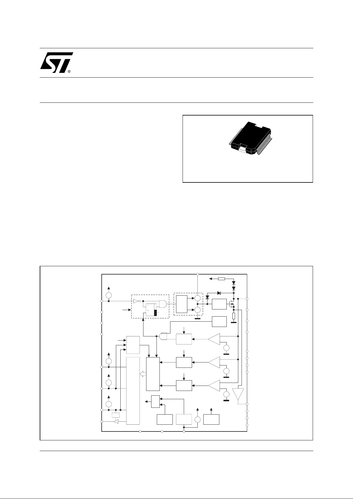
L9362
QUAD LOW SIDE DRIVER
PowerSO36
ORDERING NUMBER: L9362
■
TYPICAL INTERNAL OSCILLATOR FREQUENCY 325kHZ
DESCRIPTION
The Quad Driver is an integrated quad low-side
power switch with power limitation, load i nterrupt
and shorted load detection, thermal shutdown, error detection via SPI interface and integrated Z-diodes for output clamping, free running diodes.
BLOCK DIAGRAM
NON1
NON2
NON3
NON4
SDI
CLK
NSC
SDO
99AT0007
V
V
V
V
CC
=
Reset
CC
=
CC
=
CC
=
Reset
IRES
FR
RESET
Shift
Register
Trigger
S
R
IRES
Failure
Register
Reset ≥1
(FR)
Under
voltage
RESET
Driver
NON1
I_SCB Filter
t_SCB
NON1
I_OL Filter
t_OL
NON1
SCG Filter
t_SCG
RESET
NRESSGNDLGND
VCC
=
=
V
CC
=
V
CC
OSC
Oscillator
R
OL
dV/dt
Control
Overtemp.
OUT1
OUT2
OUT3
OUT4
=
=
=
PGND1
PGND2
PGND3
PGND4
CFB1
CFB2
CFB3
CFB4
May 2002
1/17
Page 2
L9362
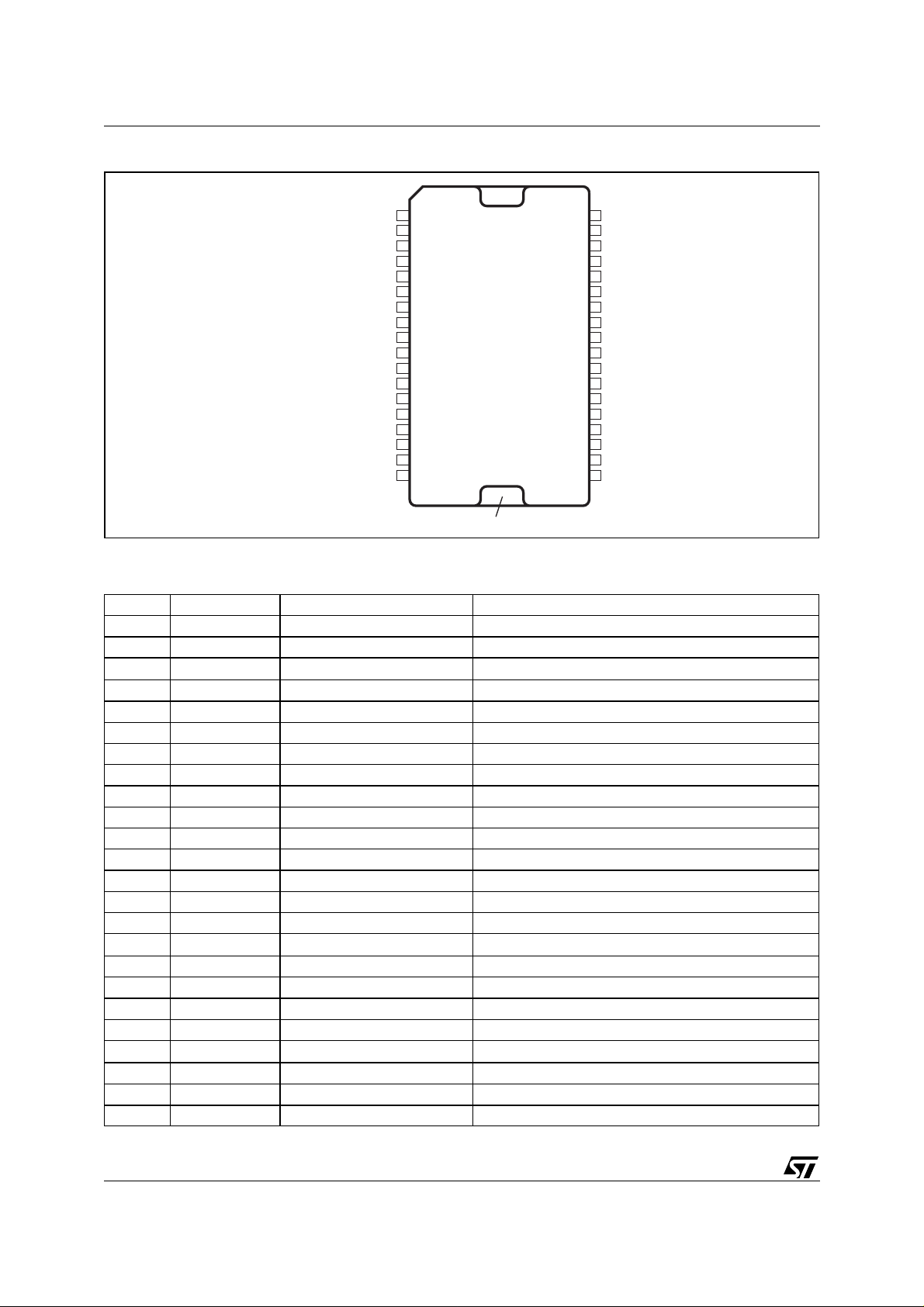
PIN CONNECTION
99AT0012
PGND1
N.C.
CFB1
OUT1
OUT1
CLK
NCS
N.C.
SGND
LGND
N.C.
SDO
SDI
OUT4
OUT4
CFB4
N.C.
PGND4
136
235
334
433
532
631
730
829
928
10 27
11 26
12 25
13 24
14 23
15 22
16 21
17 20
18
Frame connected to PGND
19
PGND2
N.C.
CFB2
OUT2
OUT2
NON1
NON2
N.C.
VCC
N.C.
NRES
NON3
NON4
OUT3
OUT3
CFB3
N.C.
PGND3
PIN FUNCTIONS
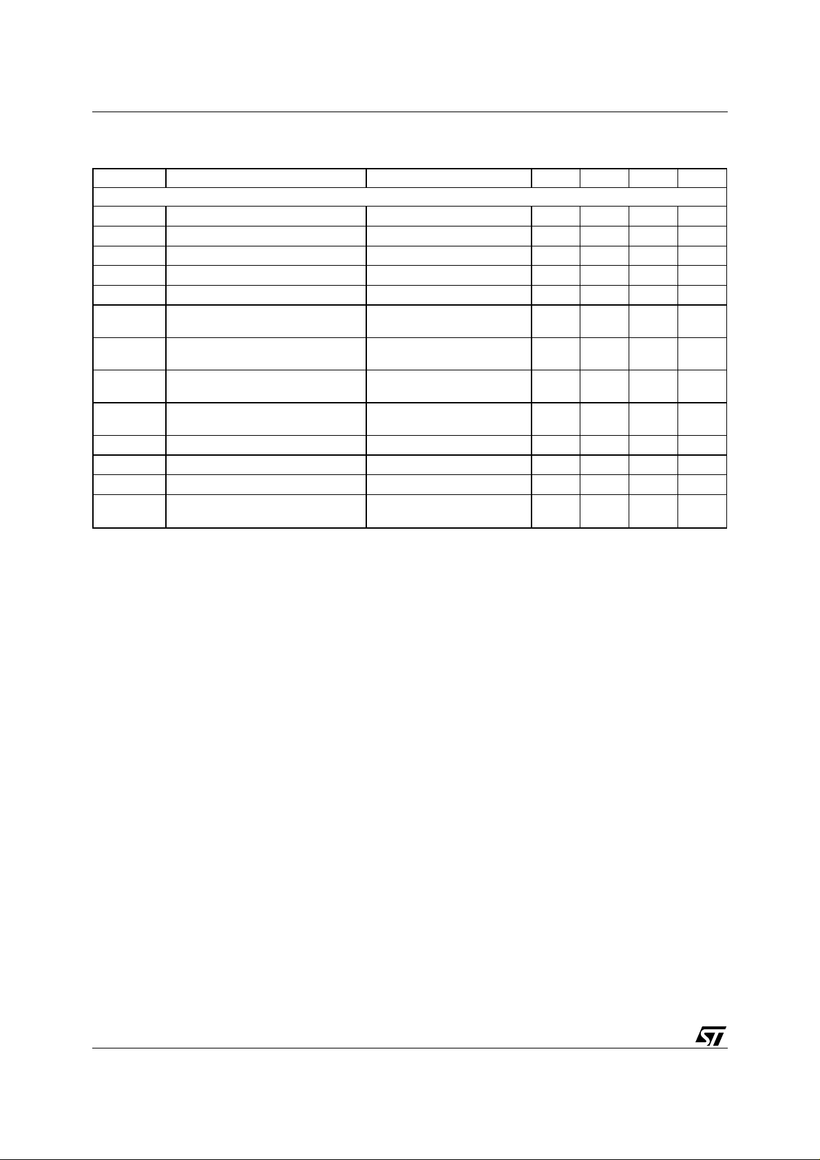
Pin No. Pin Name Pin Description Notes
1 PGND1 Power Ground
2 N.C.
3 CFB1 Output Current feedback Sinks current proportional to I
4 OUT1 Output Power Switch
5 OUT1 Output Power Switch
6 CLK Input Clock Digital input, Schmitt trigger, internal Pullup current
7 NCS inverted Chip Select Input Digital input, Schmitt trigger, internal Pullup current
8 N.C.
9 SGND Signal Ground
10 LGND Ground of digital part
11 N.C.
12 SDO Serial Data Output Digital tristate output
13 SDI Serial Data Input Digital input, Schmitt trigger, internal Pullup current
14 OUT4 Output Power Switch
15 OUT4 Output Power Switch
16 CFB4 Output Current feedback Sinks current proportional to I
17 N.C.
18 PGND4 Power Ground
19 PGND3 Power Ground
20 N.C.
21 CFB3 Output Current feedback Sinks current proportional to I
22 OUT3 Output Power Switch
23 OUT3 Output Power Switch
24 NON4 Inverted Control Signal Input Digital input, Schmitt trigger, internal Pullup current
OUT1
OUT4
OUT3
2/17
Page 3
L9362
PIN FUNCTIONS
(continued)
Pin No. Pin Name Pin Description Notes
25 NON3 Inverted Control Signal Input Digital input, Schmitt trigger, internal Pullup current
26 NRES Inverted Reset Input Digital input, Schmitt trigger, internal Pullup current
27 N.C.
28 VCC 5V Supply Voltage Input
29 N.C.
30 NON2 Inverted Control Signal Input Digital input, Schmitt trigger, internal Pullup current
31 NON1 Inverted Control Signal Input Digital input, Schmitt trigger, internal Pullup current
32 OUT2 Output Power Switch
33 OUT2 Output Power Switch
34 CFB2 Output Current feedback Sinks current proportional to I
OUT2
35 N.C.
36 PGND2 Power Ground
THERMAL DATA
Symbol Parameter Test Conditions Min. Typ. Max. Unit
Thermal resistance
R
th j-case
R
thja
R
thja
ESD
ESD MIL 883C ±2KV
Thermal resistance junction to case
(one powerstage in use)
Die must be
soldered on the
4.5 °C/W
frame.
Thermal resistance junction-ambient pad layout 50 °C/W
Thermal resistance junction-ambient
pad layout + 6 cm
2
35 °C/W
on board heat sink
ABSOLUTE MAXIMUM RATINGS
For externally applied voltages or currents exceeding these limits damage of the circuit may occur
Symbol Parameter Test Conditions Min. Typ. Max. Unit
Supply Voltages
V
CC
Outputs (Out 1 ... 4)
V
Out
I
outc
I
SCBpeak
W
OFF
Inputs (NONx; NCS; CLK; NRES; SDI)
V
IN
Outputs (SDO; CFB)
V
OUT
Operating junction temperature
T
Note: The maxi mum ratings may not be exceeded under an y circumstanc es, not even moment arily and individ ually, as perman ent
Supply voltage -0.3 7 V
Continues output voltage With no reverse
-0.3 45 V
current.
Continues current 3.0 A
Peak output current -10 I_SCB A
Clamped energy at the switching OFF For 2ms, see fig. 8 50 mJ
Input voltage -0.3 7 V
Output voltage -0.3 V
Operating junction temperature -40 150 °C
j
damage to the IC will result.
CC
+0.3
V
3/17
Page 4
L9362
ELECTRICAL CHARACTERISTICS
≤
VCC ≤ 5.5V, -40°C ≤ TJ ≤ 125°C, unless otherwise specified.
4.5V
Symbol Parameter Test Conditions Min. Typ. Max. Unit
Supply current
I
CCRES
Standby current Without load.
≤ 85°C
T
j
NRES = LOW
I
CCOPM
I
CCLV
Operating mode I
OUT 1 ... 4
= 2A 11 17 mA
Low voltage supply current VCC < 0,5V 80 µA
Inputs (NONx; NCS; CLK; NRES; SDI)
V
INL
V
INH
V
hyst
I
IN
I
IN
Low threshold -0.3 0.2 •
High threshold 0.7 •
Hysteresis 0.85 V
Input leakage current VIN = V
Input current (NONx, NCS, CLK,
V
IN
CC
≤ 0.8•V
CC
SDI)
I
IN NRES
Input current NRES 3 20 µA
Serial Data Output
V
V
I
SDOL
SDOH
SDOL
High output level (I
Low output level (I
= -2mA) V
SDO
= 3.2mA) 0.4 V
SDO
Tristate leakage current (NCS = HIGH;
= 0V ... VCC)
V
SDO
Outputs (Out 1 ... 4)
I
OUTL1
Leakage current 1 (NON = HIGH;
= 14V;
V
OUT
VCC = 5V)
V
W
R
DSON
OVR
OVR
OVR
clpa
OFF
Output clamp voltage V
Clamped energy at the switching
1)
OFF
ON resistance I
Positive output voltage ramp
p1
(with inductive load)
p2
Negative output voltage ramp 80% ... 30% of V
n
(I
clpa
= 0.5A) 45 50 60 V
OUT
For 2ms, see fig. 8 50 mJ
= 2A; Tj = 150°C;
OUT
Tj = 25°C
V
OUT
V
BAT
V
OUT
V
BAT
2)
= 30% ... 80% of
=16V 3)
=
... 0.9 • V
clp
with inductive load
t
dON
t
dOFF
Note 1: Typical lo ads for the zener clamping and the out put voltage ramps are:
Note 2: At 150°C gu aranteed by design and el ectrical characteri sation
Note 3: Tested with resistive load of R
Turn ON delay NON = 50%;
V
OUT
Turn OFF delay NON = 50%;
V
OUT
a) 10Ω, 16mH at all outputs or
b) 25Ω, 160mH
Ω
= 50
load
= 0.8 • V
= 0.3 • V
BAT
BAT
3)
BAT
= 16V
3)
V
CC
20 100 µA
CC
- 0.4
-10 10 µA
250
0.3
0.9 1.35
0.75
0.3 0.9 1.35 V/µs
0410µs
0410µs
1.3 mA
V
CC
V
CC
+0.3
10 µA
10 µA
500
300
2.25
V
V
V
mΩ
mΩ
V/µs
V/µs
4/17
Page 5

L9362
ELECTRICAL CHARACTERISTICS
≤
4.5V
VCC ≤ 5.5V, -40°C ≤ TJ ≤ 125°C, unless otherwise specified.
(continued)
Symbol Parameter Test Conditions Min. Typ. Max. Unit
Powerstage protection
I
SCB
Short current detection and switch
With filter-time t_SCB. 3.0 5.0 A
off threshold
t_SCB Short circuit switch off delay time 3 30 µs
V
ccmin
VCC undervoltage 3.0 4.0 V
Current feedback
T
Ratio 1ICFB
6)
T
MPS1
/ I
for I
OUT
5)
OUT
=0.4...2A
4)
V
≥ 1.8V 1.45 1.65 2 mA/A
CFB
Temperature stability
±3 ±6%
for 0.4A to < 2.0A, related to
25°C
CURS1
CURlin1
CURlin2
= 0.4A to 2A
for I
OUT
6)
for I
= 0.4A to 1.0A
OUT
for I
= 1.0A to 2.0A
OUT
5)
4)
4)
Current stability
∆gain/Gain at 2A
= -40°C -12 17 %
T
J
= +25°C -6 10 %
T
J
= +125°C -5 5 %
T
J
Linearity Error
(within the calibration points
±0.2 ±1
±0.7
at 0.5A, 1A, 2A)
Note 4: At 150°C gu aranteed by design and el ectrical characteri sation
Note 5: Guaranteed by design and electri cal charact erisatio n
Note 6: Values for T
, CURlin1 and CURlin2 are typical values from testing results
MPS1
Diagnostic
V
REF1
Short to GND threshold voltage for I
≤ 2A 0.390
OUT
•V
CC
0.435
•V
CC
t_SCG Short to GND filter time 140 250 µs
I
OL
Open load threshold current 10 55 mA
t_OL Open load filter time 140 265 µs
R
OL
Pullup resistor at OUT1, OUT2,
2.0 8.0 kΩ
OUT3 and OUT4 for OL detection
T
OFF
Note 7: Guaranteed by meas urement and correlati on
Temperature detection threshold
7)
155 170 190 °C
%
%
V
5/17
Page 6
L9362
ELECTRICAL CHARACTERISTICS
≤
4.5V
VCC ≤ 5.5V, -40°C ≤ TJ ≤ 125°C, unless otherwise specified.
(continued)
Symbol Parameter Test Conditions Min. Typ. Max. Unit
Serial diagnostic link (external Load capacitor at SDO = 100pF)
f
t
clh
t
t
pcld
t
csdv
t
sclch
clk
cll
Clock frequency 50% duty cycle. 0 3 MHz
Minimum time CLK = HIGH 100 ns
Minimum time CLK = LOW 100 ns
Propagation delay CLK to data at SDO valid. 100 ns
NCS = LOW To data at SDO valid. 100 ns
CLK low before NCS low Setup time CLK to NCS
100 ns
change H/L.
t
hclcl
CLK change L/H after
100 ns
NCS = LOW
t
scld
SDI input setup time CLK change H/L after SDI
20 ns
data valid.
t
hcld
SDI input hold time SDI data hold after CLK
20 ns
change H/L.
t
sclcl
t
hclch
t
pchdz
t
fNCS
CLK low before NCS high 150 ns
CLK high after NCS high 150 ns
NCS L/H to output data float 100 ns
NCS filter-time Pulses ≤ t
fNCS
will be
10 40 ns
ignored.
Note: 8. Input Pin Capacitance of SDI, CLK, NCS, NON1, NON2, NON3, NON4 6pF typical; Output Pin Capacitance of SDO 12pF typica
6/17
Page 7

1.0 Diagnostic Register and SPI timing
Figure 1. Impulse diagram to read the Diagnostic Register
NCS
CLK
L9362
LSBFSL D1 D6D4D3 D5 MSB
D2SDO
SDI LSB D1 D2 D3 D4 D5
FR_RESET
99AT0008
Note: FR_RESET means Reset failure storage (internal signal)
Figure 2. Diagnostic Failure Register Structure
MSB LSB
D5D7 D6 D1D3D4 D2 D0 FSL
Failure indicator bit
(only valid during NCS = LOW
to the first L to H CLK change
1: failure stored
0: no failures
D6 MSB
99AT0009/A
Status channel 4
D0 D1 Status
1 1 no failures
1 0 open circuit, channel on
0 1 short to battery or overtemperature
0 0 short to gnd, channel off
Status channel 3
D2 D3 corresponding to D0 D1
Status channel 2
D4 D5 corresponding to D0 D1
Status channel 1
D6 D7 corresponding to D0 D1
7/17
Page 8

L9362
Figure 3. Timin g of the Serial Interfac e
NCS
t
sclch
t
hclcl
t
clh
t
cll
CLK
t
pcld
FSL
t
D0
t
scld
hcld
D0 D1 D7
SDO
SDI
99AT0010
t
csdv
Figure 4. Short-Circuit to GND Failure (SCG-Failure) Detection
t
t
sclcl
t
pchdz
D7
Failure-detection time
for a SCG-failure
hclch
OFF
NON
ON
V
V
drain
drain
< V
V
ref
ref
at OFF-state
t_SCG (filter-time)
Failure-detection
Failure-store
00AT0002
SCG-failure
Filter-time
8/17
Page 9

Figure 5. Open-Load Failure (OL-Failure) Detection
Sporadical failure-detection Statical failure-detection
Failure detection active
for a sporadical OL-failure
L9362
NON
Lload
Lload > I_OL
Diagnostic active
t_OL (filter-time)
Failure-detection
Failure-store
00AT0003
OFF
ON
I_OL
Retrigger
t filter
Lload > I_OL
for t > t_OL
t_OL
Retrigger
filter
t < t_OL
Sporadical
failure-detection
9/17
Page 10

L9362
Figure 6. Different cases for an Open Load failure detection (case 1 to 10)
CASE 1
Non Input
Failure Register
Status
CASE 2
Non Input
Failure Register
Reset
Output
Current
Failure Register
Status
CASE 3
Output
Current
Failure Register
Status
CASE 4
Output
Current
Failure Register
Status
CASE 5
Output
Current
Failure Register
Status
CASE 6
Output
Current
Failure Register
Status
CASE 7
Output
Current
Failure Register
Status
CASE 8
Output
Current
Failure Register
Status
CASE 9
Output
Current
Failure Register
Status
CASE 10
Output
Current
Failure Register
Status
00AT0004
IOL = OL filter time
IOL
IOL
IOL
IOL
IOL
IOL
IOL
IOL
IOL
t
OL
t
OL
t
OL
t
OL
t
OL
t
OL
t
OL
t
OL
t
OL
t
t
OL
t
OL
t
OL
t
OL
t
OL
t
OL
t
OL
t
OL
t
OL
OL
t
OL
10/17
Page 11

Figure 7. Different cases for an Open Load failure detection (case 11 to 20)
L9362
CASE 11
Output
Current
Failure Register
Status
CASE 12
Output
Current
Failure Register
Status
CASE 13
Output
Current
Failure Register
Status
CASE 14
Output
Current
Failure Register
Status
CASE 15
Output
Current
Failure Register
Status
CASE 16
Output
Current
Failure Register
Status
CASE 17
Output
Current
Failure Register
Status
CASE 18
Output
Current
Failure Register
Status
CASE 19
Output
Current
Failure Register
Status
CASE 20
Non Input
IOL
IOL
IOL
IOL
IOL
IOL
IOL
IOL
IOL
t
OL
t
OL
t
OL
t
OL
t
OL
t
OL
t
OL
t
OL
t
OL
t
OL
t
OL
t
OL
t
OL
t
OL
t
OL
t
OL
t
OL
t
OL
t
OL
t
OL
t
OL
Failure Register
Reset
Output
Current
Failure Register
Status
00AT0005
IOL
t
OL
t
OL
t
OL
t
OL
t
OL
11/17
Page 12

L9362
Figure 8. Max Clamp Energy Specification
1000
800
600
400
Energy/[mJ]
200
0
0.0 2.0 4.0 6.0 8.0 10.0
Temp=25˚C
Temp=150˚C
Pulse width/[ms]
Figure 9. Tratio of Current Feedback output versus output curr ent
1.80e-03
1.75e-03
1.70e-03
1.65e-03
1.60e-03
1.55e-03
Tratio
1.50e-03
1.45e-03
1.40e-03
1.35e-03
1.30e-03
0.0 0.2 0.4 0.6 0.8 1.0 1.2 1.4 1.6 1.8 2.0
IOUT/[A]
Temp=-40˚C
Temp=-20˚C
Temp=25˚C
Temp=70˚C
Temp=150˚C
12/17
Page 13

L9362
Figure 10. TMPS1 vs. Temperature
3
2
1
0
TMPS1/[%]
-1
-2
-3
-50 0
(4.5V ≤ V
≤ 5.5V; 0.5A ≤ I
cc
out1...4
≤ 3A)
.
50 100 150 200
Temp./[˚C]
FUNCTIONAL DESCRIPTION
Introduction
The Quad Low Side Driver UF07 is built up of four identical channels (Low Side Drivers), controlled by four
CMOS input stages. Each Channel is protected against short to V
A diagnostic logic recognizes four failure types at the output stage: overcurrent, short to GND, open-load and
overtemperature.
The failures are stored individually for each channel in one byte which can be read out via a serial interface (SPI).
Each channel has a current feedback output which sinks a current proportional to the load current of the Low
Side Switch.
Output Stage Control
Each of the four output stages is switched ON and OFF by an individual control line (NON-Input). The logic level of
the control line is CMOS compatible. The output transist ors are switched off when the inputs are not connected.
Power Transistors
Each of the four output stages has its own zener clamp. This caus es a voltage limitation at the power transi stors
when inductive loads are switched off. Output voltage ramp occurring when the output is switched on or off, is
within defined limits. Output transistors can be connected in parallel to increase the current capability. In this
case, the associated inputs, outputs and current feedback outputs should be connected together.
Diagnostics
Following failures at the output stage are recognized:
Short circuit to V
Short circuit to GND...................................=SCG
Open Load.................................................= OL (Lowest Priority)
or overtemp................= SCB (Highest priority)
Bat
and by a zener clamp against overvoltage.
Bat
13/17
Page 14

L9362
Short-Circuit and Overtemperature Protection (SCB)
If the output current increases above the short current limit for a longer time than t_SCB or if the temperature
increases above T
control signal at the NON-Input is switched off and on again. This filter time has the purpose to suppress wrong
detection on short spikes.
All four outputs have an independent overtemperature detection and shutdown. This measurement is active
while the powerstage is switched on.
The Short circuit detection and the overtemperature detection are using the same bit in the Diagnostic (one for
each channel).
SCG
A
failure will be recogni zed, when the drain voltage of the output s tage is lower as the “Short Cut to Ground
threshold voltage”, while the output stage is switched off (see Fig. 4). The SCG failure is filtered with a digital
filter (t_SCG) to suppress the storage of a failure at small SCG spikes, which are typical during the transition of
the power output. This filter is triggered by the NON input and the (analog) SCG detection.
If the current through the output stage is lower than the IOL-reference, then an
after a filter time. This measurement is active while the powerstage is switched on.
The Open Load failure detection has 2 different modes, the statical failure detection and the sporadic failure
detection. One main difference is, that a statical failure is transferred to the Failure register with the next rising
edge of NON, whereas a sporadic failure is transferred immediately to the Failure register (see fig. 5, 6 and 7).
In both failure modes the OL detection is filtered (t_OL=t
same digital filter for suppression of spikes.
The failures are stor ed regar ding to their prior ity (see above). A fai lure wi th a higher prior ity ov erwrites an eventually already detected failure with a lower priority.
, then the power transistor is immediately switched off. It remains switched off until the
OFF
OL
failure will be recognized
) and is using together with the SCG detection the
OL
Diagnostic interface
The communication between the microprocessor and the failure register runs via the SPI li nk. If there is a failure
stored in the fail ure r egis ter, the fir st bit of the shift register i s set to a high lev el. With the H /L change at the NCS
pin the first bit of the di agnostic shift regi ster wi ll be trans mitted to the SDO output. The SDO output is the s erial
output from the diagnostic shift register and i t is tristate w hen the NCS pin is high. The C LK pin clock s the diagnostic shift register. New SDO data will appear on every rising edge of the CLK pin and new S DI data will be
latched on every falling edge into the shift register. With the first positive pulse of the CLK the contents of the
failure register is copied to the SPI shift register and a internal reset (FR_RESET) is generated. This internal
reset clears the failure register and thus the failure register is capable of detecting failures also during the SPI
read cycle. T here i s no bus colli sion at a s mall spik e at the NCS. The CLK has to be LOW, w hile the N CS si gnal
is changing.
Current feedback
Each channel has a current feedback output which sinks a current proportional to the load current of the Low
Side Switch. Using this output servo loop applications can be realized by applying a PWM signal to the NON
input. A typical diagram of the Current Feedback output at different temperatures is shown in figure 9.
14/17
Page 15

Reset
There are two different reset functions realized:
Undervoltage reset
As long as the voltage of Vcc is lower than V
, the powerstages are switched off, the failure register
ccmin
is reset and the SDO output remains tristate.
External reset
As long as the NRES pin is low following circuits are reset:
Powerstages
Failure register
and the SDO output is tristate.
Under volta ge protectio n
At Vcc below V
the device remains switched off even if there is a voltage ramp at the OUT pin.
ccmin
Figure 11. Ap plication Cir cuit
V
CC
V
CC
=
NON1
NON2
NON3
NON4
µC
SDI
CLK
NSC
SDO
Reset
V
CC
=
V
CC
=
V
CC
=
IRES
Reset
RESET
Shift
Register
FR
Trigger
S
R
IRES
Failure
Register
(FR)
Reset ≥1
Under
voltage
RESET
C1
Driver
NON1
I_SCB Filter
t_SCB
NON1
I_OL Filter
t_OL
NON1
SCG Filter
t_SCG
RESET
NRESSGNDLGND
C2
=
=
V
VCC
CC
=
V
CC
dV/dt
Control
Overtemp.
OSC
Oscillator
L9362
V
S
R
OL
OUT1
C
1
OUT2
C
2
OUT3
C
OUT4
=
=
=
PGND1
PGND2
PGND3
PGND4
CFB1
CFB2
CFB3
CFB4
3
C
(optional
for all
channels)
4
V
CC
ADC
99AT0011
15/17
Page 16

L9362
DIM.
MIN. TYP. MAX. MIN. TYP. MAX.
mm inch
A 3.60 0.141
a1 0.10 0.30 0.004 0.012
a2 3.30 0.130
a3 0 0.10 0 0.004
b 0.22 0.38 0.008 0.015
c 0.23 0.32 0.009 0.012
D (1) 15.80 16.00 0.622 0.630
D1 9.40 9.80 0.370 0.385
E 13.90 14.50 0.547 0.570
e 0.65 0.0256
e3 11.05 0.435
E1 (1) 10.90 11.10 0.429 0.437
E2 2.90 0.114
E3 5.80 6.20 0.228 0.244
E4 2.90 3.20 0.114 0.126
G 0 0.10 0 0.004
H 15.50 15.90 0.610 0.626
h 1.10 0.043
L 0.80 1.10 0.031 0.043
N10°(max.)
S8°(max.)
(1): "D" and "E1" do not include mold flash or protrusions
- Mold flash or protrusions shall not exceed 0.15mm (0.006 inch)
- Critical dimensions are "a3", "E" and "G".
OUTLINE AND
MECHANICAL DATA
PowerSO36
NN
a2
A
1936
0.12 AB
⊕
e
M
E1
DETAIL B
lead
a3
B
Gage Plane
PSO36MEC
BOTTOM VIEW
DETAIL B
0.35
S
E
DETAIL A
L
E2
h x 45˚
DETAIL A
118
A
e3
H
D
b
c
a1
slug
E3
D1
- C -
SEATING PLANE
GC
(COPLANARITY)
16/17
Page 17

L9362
Information furnished is believed to be accurate and reliable. However, STMicroelectronics assumes no responsibility for the consequences
of use of such information nor for any infringement of patents or other rights of third parties which may result from its use. No license is granted
by implic ation or otherwise under any patent or patent r i ghts of STM i croelectr oni cs. Specifications menti oned in th i s publicati on are subject
to change without notice. This publication supersedes and replaces all information previously supplied. STMicroelectronics products are not
authorized for use as cri tical components in li f e support dev i ces or systems without express writ t en approval of STMicroe l ectronics.
The ST logo is a registered trademark of STMicroelectronics
2002 STMi croelectronics - All Ri ghts Rese rved
Australia - Brazi l - Canada - Ch i na - F i nl and - Franc e - Germany - Hong Kong - India - Israel - I taly - Japan -M alaysia - Malta - Morocco -
Singap ore - Spain - Sw eden - Switzerland - U ni ted Kingdom - United St at es.
STMicroelectronics GROUP OF COMPANIES
http://www.s t. com
17/17
 Loading...