

Page 1
PRELIMINARY DATA
p
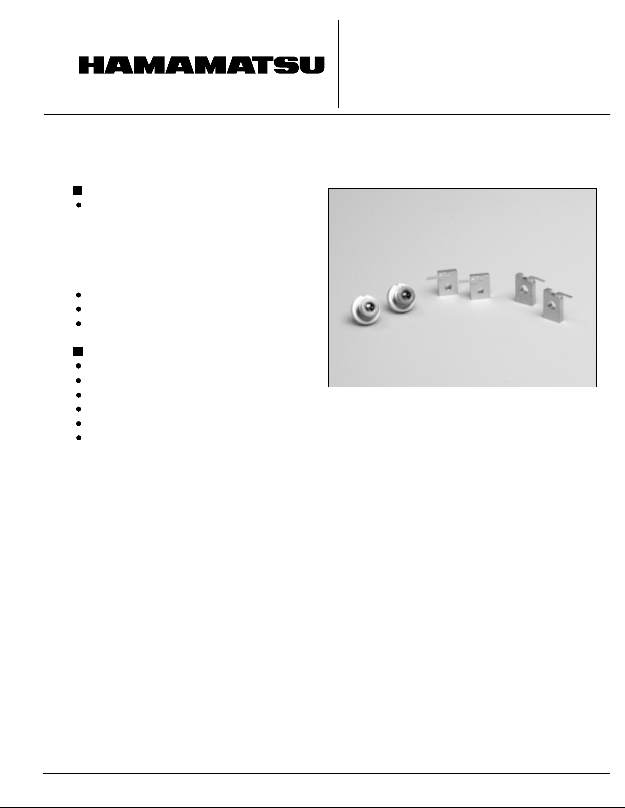
High optical power from a single chip
FEATURES
High optical power & high radiant flux
density(CW)
L8933 series : 0.5 W / 50 µm
L8446 series : 1 W / 100 µm
L8763 series : 1 W / 50 µm
L8828 series : 2 W / 100 µm
High stability
Long life
Compact
CW LASER DIODES
L8933 , L8446 , L8763 , L8828 SERIES
APPLICATIONS
Pumping source for solid state lasers
Printing
Medical instrument
Measuring instrument
Material Processing
Marking
HAMAMATSU CW laser diodes, L8933, L8446, L8763, L8828 series feature high optical power of 0.5 to 2.0 W
under CW operation. As this is single chip and single element type, emitting area is small (50 µm to 100 µm X 1
µm). Therefore, it is easy to focus on to a small spot with optics. It can be used for various applications such as
pumping of solid lasers, printers, medical instruments etc.
Information furnished by HAMAMATSU is believed to be reliable. However, no responsibility is assumed for possible inaccuracies or omissions.
ecifications are subject to change without notice. No patent rights are granted to any of the circuits described herein. '2003 Hamamatsu Photonics K.K.
S
Page 2
CW LASER DIODES L8933 , L8446 , L8763 , L8828 SERIES
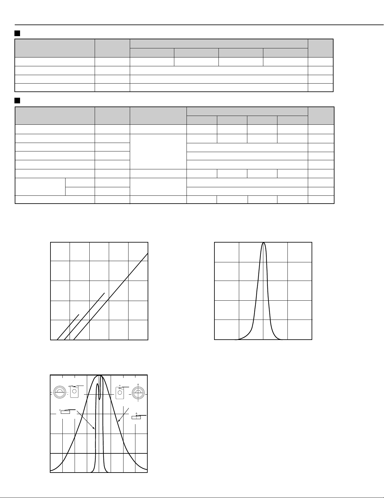
ABSOLUTE MAXIMUM RATINGS (Top(c) = 25 °C)
Parameter
Radiant Output Power
Reverse Voltage
Operating Temperature
Storage Temperature
Symbol
Φ
e
V
r
T
op(c)
T
stg
L8933
0.6
L8446
1.2 1.2
Value
2
0 to +30
-30 to +80
L8763
L8828
2.2
CHARACTERISTICS (Top(c) = 25 °C)
Parameter Symbol
Radiant Output Power
Forward Current
Peak Emission Wavelength
Spectral Radiation Half Bandwidth
Forward Voltage
Emitting Area Size
Parallel
Beam Spread Angle
Vertical
Lasing Threshold Current
*1
Tolerance of of peak emission wavelength can be selected from +/- 3nm, +/- 5nm and +/- 10nm for every type of laser diodes listed above. For its details, see the
table of SUFFIX in the next page.
Other laser diodes of different peak emission wavelength are available, such as 830nm, 940nm and 980nm. Contact your local representative for more information.
Φ
λ
∆λ
V
θ
θ
I
e
I
f
p
f
-
//
⊥
th
Conditions
-
L8933 Φ
L8763 Φ
L8446 Φ
L8828 Φ
= 0.5 W
e
= 1 W
e
= 1 W
e
= 2 W
e
Value at designing
FWHM
-
L8933
0.5
0.65
808 ± 3 , 808 ± 5 , 808 ± 10 *1
X 1
50
0.15
L8446
1
1.2
100 X 1
0.35
Value
2
2
8
32
L8763
1
1.2
X 1
50
0.35
L8828
2
2.4
100 X 1
0.6
Unit
W
V
°C
°C
Unit
W
A
nm
nm
V
µm
degree
degree
A
Figure 1:
Radiant Output Power vs. Forward Current (Typ.)
2.5
2.0
(W)
e
1.5
1.0
L8933
0.5
Radiant Output Power Φ
0
0
0.5 1.0
Forward Current I
Figure 3: Directivity (Typ.)
100
80
60
Parallel
Direction
Top View
Parallel
Direction
Top View
Parallel
Direction
Side View
L8763
L8446
1.5
( Top(c) = 25 °C )
2.0
(A)
f
op(c) = 25 °C )
(T
Vertical
Direction
Side View
Top View
L8828
Vertical
Direction
Top View
Vertical
Direction
2.5
Figure 2: Emission Spectrum (Typ.)
100
80
60
40
20
Relative Radiant Output Power (%)
0
804
806
Wavelength (nm)
808
( Top(c) = 25 °C )
810
812
40
20
Relative Radiant Output Power (%)
0
3040 20 10 0 10 20 30 40
Angle (degree)
Page 3
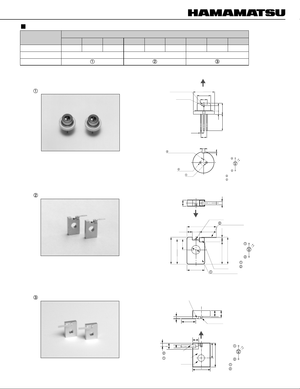
SUFFIX / DIMENSIONAL OUTLINE (Unit : mm)
Parameter
Peak Emission Wavelength (nm)
####-04
L
808 ± 3
Package
L
####
808 ± 5
φ 9.0 CD
-41
L
####
-42
808 ± 10
L
####
808 ± 3
Dimensional Outline
* φ9.0CD package is not available with 2W type L8288 series.
Pigtailed type is available as custom option. Contact your local representative for details.
φ 9.0 CD Package
Suffix
-06
L
####
808 ± 5
Side-out OHS
-61
L
####
-62
808 ± 10
Glass Window
LD Chip
L
####
808 ± 3
-07
L
####
808 ± 5
Head-out OHS
Output
+0
φ9.0
-0.1
φ5.7±0.2
φ2.8±0.3
2.41.5
-71
L
####
-72
808 ± 10
L8933-04 , L8446-04 , L8763-04
L8933-41 , L8446-41 , L8763-41
L8933-42 , L8446-42 , L8763-42
Side-out OHS Package
L8933-06 , L8446-06 , L8763-06 , L8828-06
L8933-61 , L8446-61 , L8763-61 , L8828-61
L8933-62 , L8446-62 , L8763-62 , L8828-62
Anode (Case)
Cathode
2
Output
1.8
3.8
9.4
8.8
NC
φ0.45
φ
7.0±0.5 5.1±0.5
φ
2.54
1.0
(Connection)
0.4
Anode
Cathode
LD Chip
10
5.82.4
3
6
Cathode Lead
0.15 1
1.5
7.8
Isolator
Anode Block
(Connection)
9.45
Anode
Cathode
Head-out OHS Package
L8933-07 , L8446-07 , L8763-07 , L8828-07
L8933-71 , L8446-71 , L8763-71 , L8828-71
L8933-72 , L8446-72 , L8763-72 , L8828-72
1.0
Cathode Lead
Anode Block
2.0
Isolator
0.6
0.15
2.0
2.4
6.0
LD Chip
Output
(Connection)
5.0
8.0
Anode
Cathode
5.0
2.0
1.0
φ2.2
Page 4

)
CW LASER DIODES L8933 , L8446 , L8763 , L8828 SERIES
Handling precautions & instructions
1. Absolute maximum ratings
When LDs are driven exceeding its absolute maximum ratings, it will be broken instantly or it leads to degradation of performance &
reliability. Please be careful not to exceed absolute maximum ratings even only a moment. The absolute maximum ratings in this
datasheet are specified based on case temperature at 25 °C. When the operating temperature is higher, the radiant output power &
dissipation will be reduced and it affects other characteristics. When designing the operating circuitry for LDs, please surely take
absolute maximum ratings into account.
2. Protection of electrostatic discharge sensitive (ESDS) devices
The LDs may be damaged or its performance may deteriorate due to such factors as electric field, electrostatic discharges (ESD), surge
voltage, leakage voltage etc. As a countermeasure against ESD, the device, operator, work place and jigs must all be set at the same
electric potential. When handling LDs, please wear conductive finger-cap. And please take following countermeasures ;
(1) Install protection circuit for excess voltage, reverse voltage, surge voltage into power supply, measuring instrument etc.
(2) When using soldering iron, protect LDs from leakage current & electrostatic discharge from soldering iron bit.
(3) Conductive sheet, electrically grounded through 1Mohm resistor should be laid on both the work table and the floor of the working
area. In order to protect the device from ESD which accumulate on the operator or the operator s clothes, ground electrically through
1Mohm resistor and wear a wrist strap etc.
(4) Goods like parts, container to contact / approach to LDs should be materials which is taken a countermeasures for ESD.
3. Protection for stain, stress, external damage, etc.
The LDs whose suffix -06 & -07 are bare type product, vital & fragile part is naked. Dusts, expiration, finger print, sputum, condensation
bending, chip off of LD chip, re-forming of wire may leads to degradation of performance of the LDs. Please unpack, keep, handle,
operate, drive in air-conditioned clean room so that the LDs are keep away from dust & condensation. When handling, please take
enough care not to drop, not to stain any part of LDs. When dropped or stained, do not use it.
4. Heat dissipation
Reliability of LDs is deeply correlated with junction temperature. Under higher operating temperature, the reliability deteriorates sooner.
Heat dissipating device (material: Aluminum, Copper) should be attached to the base of LDs, and cooling devices (air, water, peltier etc.)
should be operate with the LDs in order to dissipate the heat from the LDs, so that the operating temperature is kept within the absolute
maximum ratings.
5. Safety for operators and users
These LDs emit invisible laser radiation. It s classified into Class 4 according to the laser product standards of the IEC 60825-1 (Safety
of laser products Part 1: Equipment classification, requirements and user s guide) and/or ANSI Z136.1 (American National Standard for
Safe Use of Lasers) etc. Direct or reflected laser beam from these LDs may damage eyes or skin by being absorbed by cells. In the
worst case, it leads to burn or loss of eyesight. The operator must not stare the emitting area of LDs, must avoid direct exposure to the
laser beam. Wear eye-protectors (glasses or goggles) against laser radiation while operating a device. Please provide adequate
information to the end-user of its classification, performances and warnings of the products using these LDs, defying the regulations of
IEC 60825-1 and/or ANSI Z136.1 etc.
http://www.hamamatsu.com
HAMAMATSU PHOTONICS K.K., Laser Group, Sales Dept.
5000, Hirakuchi, Hamakita City, Shizuoka, 434-8601, Japan, Telephone: (81)53-584-0227, Fax: (81)53-584-0228, E-mail: [email protected]
U.S.A.: Hamamatsu Corporation:360 Foothill Road, P.O. BOX 6910, Bridgewater, N.J. 08807-0910, U.S.A.Telephone: (1)908-231-0960, Fax: (1)908-231-1218 E-mail: [email protected]
Germany: Hamamatsu Photonics Deutschland GmbH: Arzbergerstr. 10, D-82211 Herrsching am Ammersee, Germany, Telephone: (49)8152-375-0, Fax: (49)8152-2658, E-mail: [email protected]
France: Hamamatsu Photonics France S.A.R.L.: 8, Rue du Saule Trapu, Parc du Moulin de Massy, 91882 Massy Cedex, France, Telephone: 33(1) 69 53 71 00, Fax: 33(1) 69 53 71 10, E-mail: [email protected]
United Kingdom: Hamamatsu Photonics UK Limited: 2 Howard Court, 10 Tewin Road, Welwyn Garden City, Hertfordshire AL7 1BW, United Kingdom, Telephone: (44)1707-294888, Fax: (44)1707-325777, E-mail: [email protected]
North Europe: Hamamatsu Photonics Norden AB: Smidesv gen 12, SE-171-41 Solna, Sweden, Telephone: (46)8-509-031-00, Fax: (46)8-509-031-01, E-mail: [email protected]
Italy: Hamamatsu Photonics Italia S.R.L.: Strada della Moia, 1/E, 20020 Arese, (Milano), Italy, Telephone: (39)02-935 81 733, Fax: (39)02-935 81 741, E-mail: [email protected]
Cat. No. LLD1010E01
JAN. 2003 IP
Printed in Japan (500
 Loading...