

Page 1

查询L7900AC SERIES供应商
L7900AC
2% NEGATIVE VOLTAGE REGULATORS
■ OUTPUT CURRENT UPTO1.5 A
■ OUTPUT VOLTAGESOF-5; -5.2;-6; -8; -12;
-15;-18; -20;-22;-24V
■ THERMAL OVERLOADPROTECTION
■ SHORTCIRCUIT PROTECTION
■ OUTPUT TRANSITION SOA PROTECTION
DESCRIPTION
The L7900AC series of three-terminal negative
regulators is available in TO-220 and D
packages and several fixed output voltages.
These regulators can provide local on-card
regulation, eliminating the distribution problems
associated with single point regulation;
furthermore, having the same voltage option as
the L7800A positive standard series, they are
particularly suited for split power supplies. In
addition, the -5.2V is also available for ECL
system. If adequate heat sinking is provided,
they can deliver over 1.5A output current.
Although designed primarily as fixed voltage
regulators, these devices can be used with
external components to obtain adjustable
voltagesand currents.
2
PAK
D2PAK
TO-220
SERIES
3
1
SCHEMATIC DIAGRAM
June 1998
1/11
Page 2

L7900AC
ABSOLUTE MAXIMUMRATINGS
Symbol Parameter Value Unit
DC Input Voltage (forVO=-5 to -18V)
V
i
OutputCurrent Internally limited
I
o
Power Dissipation Internally limited
P
tot
Operating Junction Temperature Range 0 to 125
T
op
StorageTemperature Range - 65 to 150
T
stg
(forV
= -20,-24V)
O
THERMAL DATA
Symbol Parameter D2PAK TO-220 Unit
R
thj-case
R
thj-amb
Thermal Resistance Junction-case Max
Thermal Resistance Junction-ambient Max
3
62.5
CONNECTION DIAGRAM AND ORDERING NUMBERS (top view)
-35
-40
50
3
o
o
V
V
o
C
o
C
C/W
C/W
TO-220 D2PAK
Type TO-220 D
L7905AC
L7952AC
L7906AC
L7908AC
L7912AC
L7915AC
L7918AC
L7920AC
L7922AC
L7924AC
(*) AVAILABLE IN TAPE ANDREELWITH ”-TR” SUFFIX
L7905ACV
L7952ACV
L7906ACV
L7908ACV
L7912ACV
L7915ACV
L7918ACV
L7920ACV
L7922ACV
L7924ACV
APPLICATIONCIRCUIT
2
PAK (*) Output Voltage
L7905ACD2T
L7952ACD2T
L7906ACD2T
L7908ACD2T
L7912ACD2T
L7915ACD2T
L7918ACD2T
L7920ACD2T
L7922ACD2T
L7924ACD2T
-5V
-5.2V
-6V
-8V
-12V
-15V
-18V
-20V
-22V
-24V
2/11
Page 3

L7900AC
ELECTRICAL CHARACTERISTICS FOR L7905A (refer to the test circuits, Tj= 0 to 125oC,
=-10V, Io=500 mA, Ci= 2.2 µF, Co=1µF unlessotherwise specified)
V
i
Symbol Parameter Test Conditions Min. Typ. Max. Unit
V
OutputVoltage Tj=25oC -4.9-5-5.1V
o
V
OutputVoltage Io=-5mAto-1A Po≤15 W
o
* Line Regulation Vi=-7 to -25 V Tj=25oC
∆V
o
∆V
* Load Regulation Io= 5 to 1500 mA Tj=25oC
o
I
Quiescent Current Tj=25oC3mA
d
∆I
Quiescent Current Change Io= 5 to 1000 mA 0.5 mA
d
∆I
Quiescent Current Change Vi=-8 to -25 V 1.3 mA
d
∆
V
OutputVoltage Drift Io= 5 mA -0.4 mV/oC
o
∆
T
OutputNoise Voltage B = 10Hz to 100KHz Tj=25oC 100 µV
e
N
SVR Supply Voltage Rejection ∆V
V
Dropout Voltage Io=1A Tj=25oC
d
ShortCircuitCurrent 2.1 A
I
sc
I
ShortCircuitPeak Current Tj=25oC2.5A
scp
=8 to 20 V
V
i
=-8 to -12 V Tj=25oC
V
i
= 250 to 750mA Tj=25oC
I
o
=10V f=120Hz 54 60 dB
i
=100mV
∆V
O
-4.8 -5 -5.2 V
100
50
100
50
1.4 V
mV
mV
mV
mV
ELECTRICAL CHARACTERISTICS FOR L7952A (refer to the test circuits, Tj= 0 to 125oC,
=-10V, Io=500 mA, Ci= 2.2 µF, Co=1µF unlessotherwise specified)
V
i
Symbol Parameter Test Conditions Min. Typ. Max. Unit
V
OutputVoltage Tj=25oC -5.1 -5. 2 -5. 3 V
o
V
OutputVoltage Io=-5mAto-1A Po≤15 W
o
* Line Regulation Vi=-8 to -25 V Tj=25oC
∆V
o
∆V
* Load Regulation Io= 5 to 1500 mA Tj=25oC
o
I
Quiescent Current Tj=25oC3mA
d
∆I
Quiescent Current Change Io= 5 to 1000 mA 0.5 mA
d
∆I
Quiescent Current Change Vi=-9 to -25 V 1.3 mA
d
∆
V
OutputVoltage Drift Io= 5 mA -0.5 mV/oC
o
∆
T
OutputNoise Voltage B = 10Hz to 100KHz Tj=25oC 125 µV
e
N
SVR Supply Voltage Rejection ∆V
V
Dropout Voltage Io=1A Tj=25oC
d
ShortCircuitCurrent 2.1 A
I
sc
I
ShortCircuitPeak Current Tj=25oC2.5A
scp
* Load and line regulation are specified at constant junction temperature. Changes in Vodue to heating effects must be taken into account
separately. Pulce testing with lowduty cycle isused.
=-9 to -21 V
V
i
=-9 to -13 V Tj=25oC
V
i
= 250 to 750mA Tj=25oC
I
o
=10V f=120Hz 54 60 dB
i
=100mV
∆V
O
-5 -5.2 -5.4 V
105
52
105
52
mV
mV
mV
mV
1.4 V
3/11
Page 4

L7900AC
ELECTRICAL CHARACTERISTICS FOR L7906A (refer to the test circuits, Tj= 0 to 125oC,
=-11V, Io=500 mA, Ci= 2.2 µF, Co=1µF unlessotherwise specified)
V
i
Symbol Parameter Test Conditions Min. Typ. Max. Unit
V
OutputVoltage Tj=25oC -5.88 -6 -6. 12 V
o
V
OutputVoltage Io=-5mAto-1A Po≤15 W
o
* Line Regulation Vi=-8.5to -25V Tj=25oC
∆V
o
∆V
* Load Regulation Io= 5 to 1500 mA Tj=25oC
o
I
Quiescent Current Tj=25oC3mA
d
∆I
Quiescent Current Change Io= 5 to 1000 mA 0.5 mA
d
∆I
Quiescent Current Change Vi=-9.5to -25V 1.3 mA
d
∆
V
OutputVoltage Drift Io= 5 mA -0.6 mV/oC
o
∆
T
OutputNoise Voltage B = 10Hz to 100KHz Tj=25oC 144 µV
e
N
SVR Supply Voltage Rejection ∆V
V
Dropout Voltage Io=1A Tj=25oC
d
ShortCircuitCurrent 2 A
I
sc
I
ShortCircuitPeak Current Tj=25oC2.5A
scp
=-9.5to -21.5V
V
i
=-9 to -15 V Tj=25oC
V
i
= 250 to 750mA Tj=25oC
I
o
=10V f=120Hz 54 60 dB
i
=100mV
∆V
O
-5. 76 -6 -6.24 V
120
60
120
60
1.4 V
mV
mV
mV
mV
ELECTRICAL CHARACTERISTICS FOR L7908A (refer to the test circuits, Tj= 0 to 125oC,
=-14V, Io=500 mA, Ci= 2.2 µF, Co=1µF unlessotherwise specified)
V
i
Symbol Parameter Test Conditions Min. Typ. Max. Unit
V
OutputVoltage Tj=25oC -7.84 -8 -8. 16 V
o
V
OutputVoltage Io=-5mAto-1A Po≤15 W
o
* Line Regulation Vi=-10.5to -25V Tj=25oC
∆V
o
∆V
* Load Regulation Io= 5 to 1500 mA Tj=25oC
o
I
Quiescent Current Tj=25oC3mA
d
∆I
Quiescent Current Change Io= 5 to 1000 mA 0.5 mA
d
∆I
Quiescent Current Change Vi=-11.5to -25V 1 mA
d
∆
V
OutputVoltage Drift Io= 5 mA -0.6 mV/oC
o
∆
T
OutputNoise Voltage B = 10Hz to 100KHz Tj=25oC 175 µV
e
N
SVR Supply Voltage Rejection ∆V
V
Dropout Voltage Io=1A Tj=25oC
d
ShortCircuitCurrent 1.5 A
I
sc
I
ShortCircuitPeak Current Tj=25oC2.5A
scp
* Load and line regulation are specified at constant junction temperature. Changes in Vodue to heating effects must be taken into account
separately. Pulce testing with lowduty cycle isused.
=-11.5to -23V
V
i
=-11 to -17V Tj=25oC
V
i
= 250 to 750mA Tj=25oC
I
o
=10V f=120Hz 54 60 dB
i
=100mV
∆V
O
-7. 68 -8 -8.32 V
160
80
160
80
mV
mV
mV
mV
1.1 V
4/11
Page 5
L7900AC
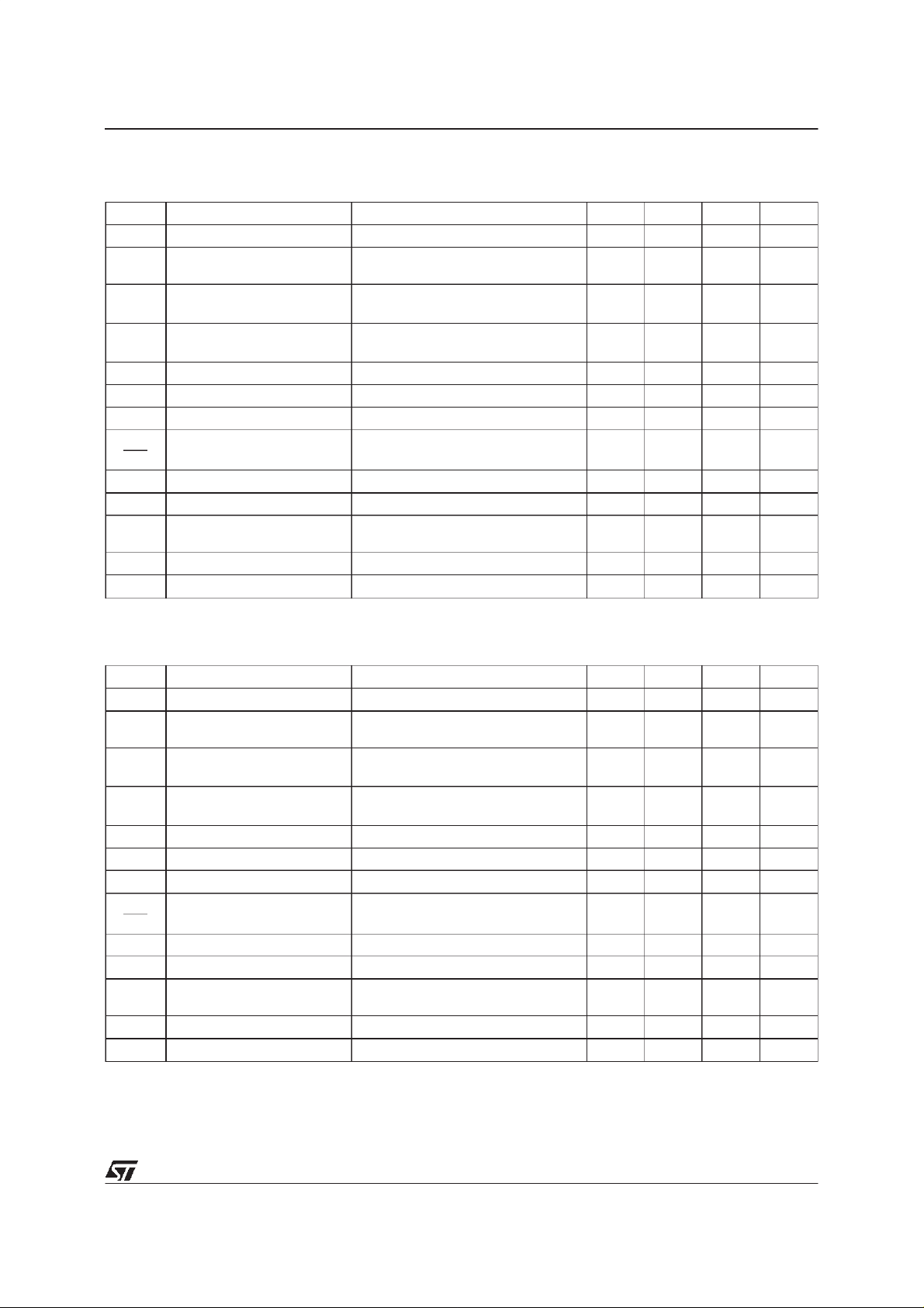
ELECTRICAL CHARACTERISTICS FOR L7912A (refer to the test circuits, Tj= 0 to 125oC,
=-19V, Io=500 mA, Ci= 2.2 µF, Co=1µF unlessotherwise specified)
V
i
Symbol Parameter Test Conditions Min. Typ. Max. Unit
V
OutputVoltage Tj=25oC -11.7 5 -12 -12.25 V
o
V
OutputVoltage Io=-5mAto-1A Po≤15 W
o
* Line Regulation Vi=-14.5to -30V Tj=25oC
∆V
o
∆V
* Load Regulation Io= 5 to 1500 mA Tj=25oC
o
I
Quiescent Current Tj=25oC3mA
d
∆I
Quiescent Current Change Io= 5 to 1000 mA 0.5 mA
d
∆I
Quiescent Current Change Vi=-15 to -25V 1 mA
d
∆
V
OutputVoltage Drift Io= 5 mA -0.8 mV/oC
o
∆
T
OutputNoise Voltage B = 10Hz to 100KHz Tj=25oC 200 µV
e
N
SVR Supply Voltage Rejection ∆V
V
Dropout Voltage Io=1A Tj=25oC
d
ShortCircuitCurrent 1.5 A
I
sc
I
ShortCircuitPeak Current Tj=25oC2.5A
scp
=-15.5to -27V
V
i
=-16 to -22V Tj=25oC
V
i
= 250 to 750mA Tj=25oC
I
o
=10V f=120Hz 54 60 dB
i
=100mV
∆V
O
-11. 5 -12 -12. 5 V
240
120
240
120
1.1 V
mV
mV
mV
mV
ELECTRICAL CHARACTERISTICS FOR L7915A (refer to the test circuits, Tj= 0 to 125oC,
=-23V, Io=500 mA, Ci= 2.2 µF, Co=1µF unlessotherwise specified)
V
i
Symbol Parameter Test Conditions Min. Typ. Max. Unit
V
OutputVoltage Tj=25oC -14. 7 -15 -15. 3 V
o
V
OutputVoltage Io=-5mAto-1A Po≤15 W
o
* Line Regulation Vi=-17.5to -30V Tj=25oC
∆V
o
∆V
* Load Regulation Io= 5 to 1500 mA Tj=25oC
o
I
Quiescent Current Tj=25oC3mA
d
∆I
Quiescent Current Change Io= 5 to 1000 mA 0.5 mA
d
∆I
Quiescent Current Change Vi=-18.5to -30V 1 mA
d
∆
V
OutputVoltage Drift Io= 5 mA -0.9 mV/oC
o
∆
T
OutputNoise Voltage B = 10Hz to 100KHz Tj=25oC 250 µV
e
N
SVR Supply Voltage Rejection ∆V
V
Dropout Voltage Io=1A Tj=25oC
d
ShortCircuitCurrent 1.3 A
I
sc
I
ShortCircuitPeak Current Tj=25oC2.3A
scp
* Load and line regulation are specified at constant junction temperature. Changes in Vodue to heating effects must be taken into account
separately. Pulce testing with lowduty cycle isused.
=-18.5to -30V
V
i
=-20 to -26V Tj=25oC
V
i
= 250 to 750mA Tj=25oC
I
o
=10V f=120Hz 54 60 dB
i
=100mV
∆V
O
-14. 4 -15 -15. 6 V
300
150
300
150
mV
mV
mV
mV
1.1 V
5/11
Page 6
L7900AC
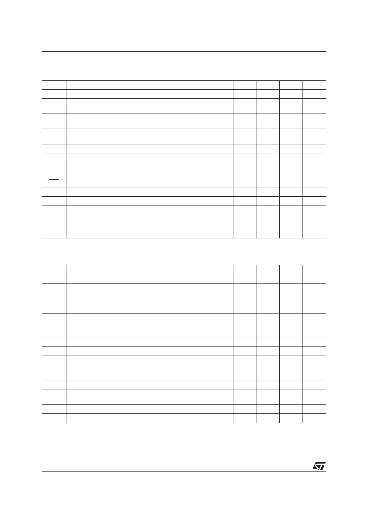
ELECTRICAL CHARACTERISTICS FOR L7918A (refer to the test circuits, Tj= 0 to 125oC,
=-27V, Io=500 mA, Ci= 2.2 µF, Co=1µF unlessotherwise specified)
V
i
Symbol Parameter Test Conditions Min. Typ. Max. Unit
V
OutputVoltage Tj=25oC -17.6 4 -18 -18.36 V
o
V
OutputVoltage Io=-5mAto-1A Po≤15 W
o
* Line Regulation Vi=-21 to -33V Tj=25oC
∆V
o
∆V
* Load Regulation Io= 5 to 1500 mA Tj=25oC
o
I
Quiescent Current Tj=25oC3mA
d
∆I
Quiescent Current Change Io= 5 to 1000 mA 0.5 mA
d
∆I
Quiescent Current Change Vi=-22 to -33V 1 mA
d
∆
V
OutputVoltage Drift Io= 5 mA -1 mV/oC
o
∆
T
OutputNoise Voltage B = 10Hz to 100KHz Tj=25oC 300 µV
e
N
SVR Supply Voltage Rejection ∆V
V
Dropout Voltage Io=1A Tj=25oC
d
ShortCircuitCurrent 1.1 A
I
sc
I
ShortCircuitPeak Current Tj=25oC2.2A
scp
=-22 to -33V
V
i
=-24 to -30V Tj=25oC
V
i
= 250 to 750mA Tj=25oC
I
o
=10V f=120Hz 54 60 dB
i
=100mV
∆V
O
-17. 3 -18 -18. 7 V
360
180
360
180
1.1 V
mV
mV
mV
mV
ELECTRICAL CHARACTERISTICS FOR L7920A (refer to the test circuits, Tj= 0 to 125oC,
=-29V, Io=500 mA, Ci= 2.2 µF, Co=1µF unlessotherwise specified)
V
i
Symbol Parameter Test Conditions Min. Typ. Max. Unit
V
OutputVoltage Tj=25oC -19. 6 -20 -20. 4 V
o
V
OutputVoltage Io=-5mAto-1A Po≤15 W
o
* Line Regulation Vi=-23 to -35V Tj=25oC
∆V
o
∆V
* Load Regulation Io= 5 to 1500 mA Tj=25oC
o
I
Quiescent Current Tj=25oC3mA
d
∆I
Quiescent Current Change Io= 5 to 1000 mA 0.5 mA
d
∆I
Quiescent Current Change Vi=-24 to -35V 1 mA
d
∆
V
OutputVoltage Drift Io= 5 mA -1.1 mV/oC
o
∆
T
OutputNoise Voltage B = 10Hz to 100KHz Tj=25oC 350 µV
e
N
SVR Supply Voltage Rejection ∆V
V
Dropout Voltage Io=1A Tj=25oC
d
ShortCircuitCurrent 0.9 A
I
sc
I
ShortCircuitPeak Current Tj=25oC2.2A
scp
* Load and line regulation are specified at constant junction temperature. Changes in Vodue to heating effects must be taken into account
separately. Pulce testing with lowduty cycle isused.
=-24 to -35V
V
i
=-26 to -32V Tj=25oC
V
i
= 250 to 750mA Tj=25oC
I
o
=10V f=120Hz 54 60 dB
i
=100mV
∆V
O
-19. 2 -20 -20. 8 V
400
200
400
200
mV
mV
mV
mV
1.1 V
6/11
Page 7
L7900AC
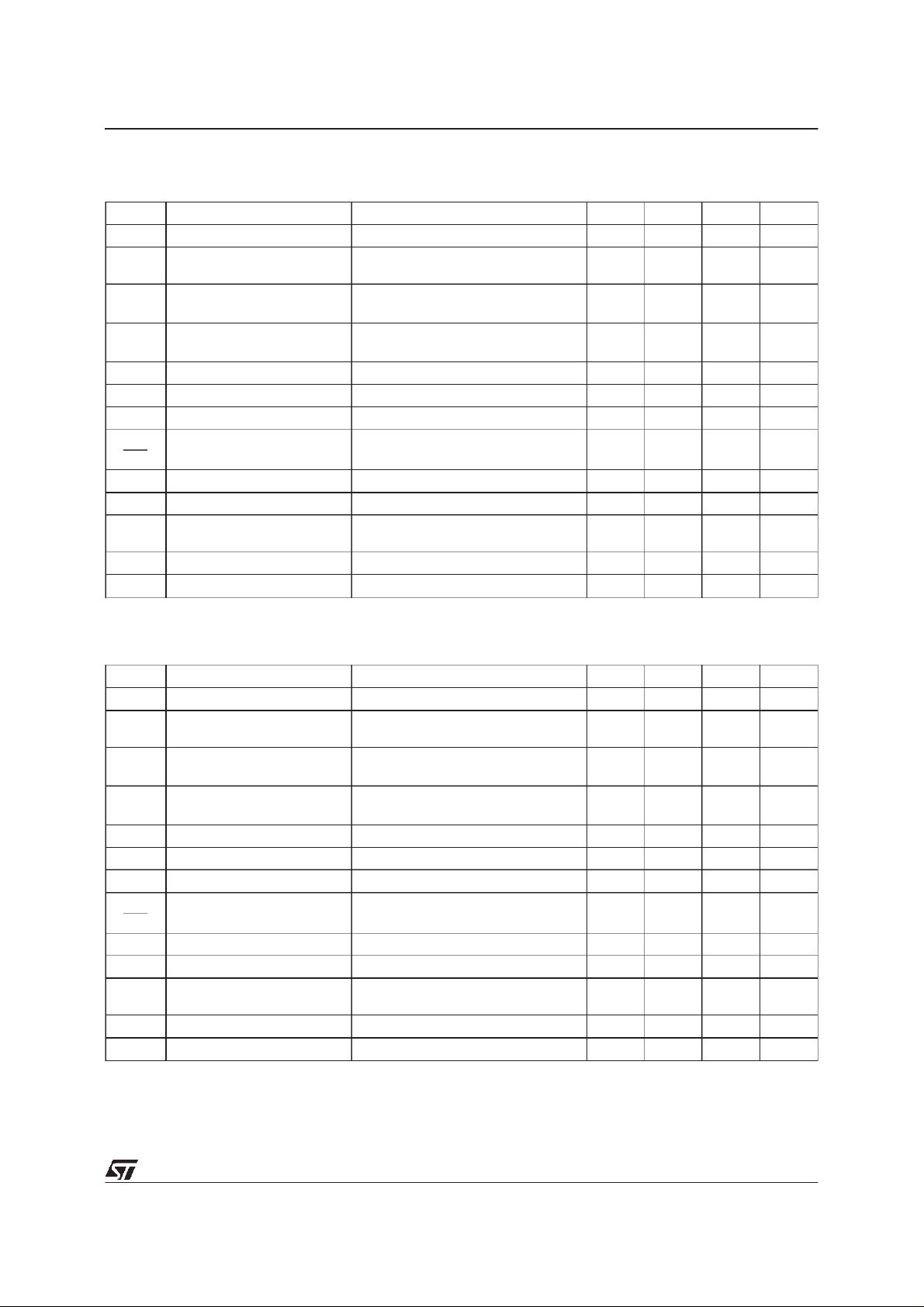
ELECTRICAL CHARACTERISTICS FOR L7922A (refer to the test circuits, Tj= 0 to 125oC,
=-31V, Io=500 mA, Ci= 2.2 µF, Co=1µF unlessotherwise specified)
V
i
Symbol Parameter Test Conditions Min. Typ. Max. Unit
V
OutputVoltage Tj=25oC -21. 5 -22 -22. 4 V
o
V
OutputVoltage Io=-5mAto-1A Po≤15 W
o
* Line Regulation Vi=-25 to -37V Tj=25oC
∆V
o
∆V
* Load Regulation Io= 5 to 1500 mA Tj=25oC
o
I
Quiescent Current Tj=25oC3mA
d
∆I
Quiescent Current Change Io= 5 to 1000 mA 0.5 mA
d
∆I
Quiescent Current Change Vi=-26 to -37V 1 mA
d
∆
V
OutputVoltage Drift Io= 5 mA -1.1 mV/oC
o
∆
T
OutputNoise Voltage B = 10Hz to 100KHz Tj=25oC 375 µV
e
N
SVR Supply Voltage Rejection ∆V
V
Dropout Voltage Io=1A Tj=25oC
d
ShortCircuitCurrent 1.1 A
I
sc
I
ShortCircuitPeak Current Tj=25oC2.2A
scp
=-26 to -37V
V
i
=-28 to -34V Tj=25oC
V
i
= 250 to 750mA Tj=25oC
I
o
=10V f=120Hz 54 60 dB
i
=100mV
∆V
O
-21. 1 -22 -22. 8 V
440
220
440
220
1.1 V
mV
mV
mV
mV
ELECTRICAL CHARACTERISTICS FOR L7924A (refer to the test circuits, Tj= 0 to 125oC,
=-33V, Io=500 mA, Ci= 2.2 µF, Co=1µF unlessotherwise specified)
V
i
Symbol Parameter Test Conditions Min. Typ. Max. Unit
V
OutputVoltage Tj=25oC -23. 5 -24 -24. 5 V
o
V
OutputVoltage Io=-5mAto-1A Po≤15 W
o
* Line Regulation Vi=-27 to -38V Tj=25oC
∆V
o
∆V
* Load Regulation Io= 5 to 1500 mA Tj=25oC
o
I
Quiescent Current Tj=25oC3mA
d
∆I
Quiescent Current Change Io= 5 to 1000 mA 0.5 mA
d
∆I
Quiescent Current Change Vi=-27 to -38V 1 mA
d
∆
V
OutputVoltage Drift Io= 5 mA -1 mV/oC
o
∆
T
OutputNoise Voltage B = 10Hz to 100KHz Tj=25oC 400 µV
e
N
SVR Supply Voltage Rejection ∆V
V
Dropout Voltage Io=1A Tj=25oC
d
ShortCircuitCurrent 1.1 A
I
sc
I
ShortCircuitPeak Current Tj=25oC2.2A
scp
* Load and line regulation are specified at constant junction temperature. Changes in Vodue to heating effects must be taken into account
separately. Pulce testing with lowduty cycle isused.
=-27 to -38V
V
i
=-30 to -36V Tj=25oC
V
i
= 250 to 750mA Tj=25oC
I
o
=10V f=120Hz 54 60 dB
i
=100mV
∆V
O
-23 -24 -25 V
480
240
480
240
mV
mV
mV
mV
1.1 V
7/11
Page 8
L7900AC
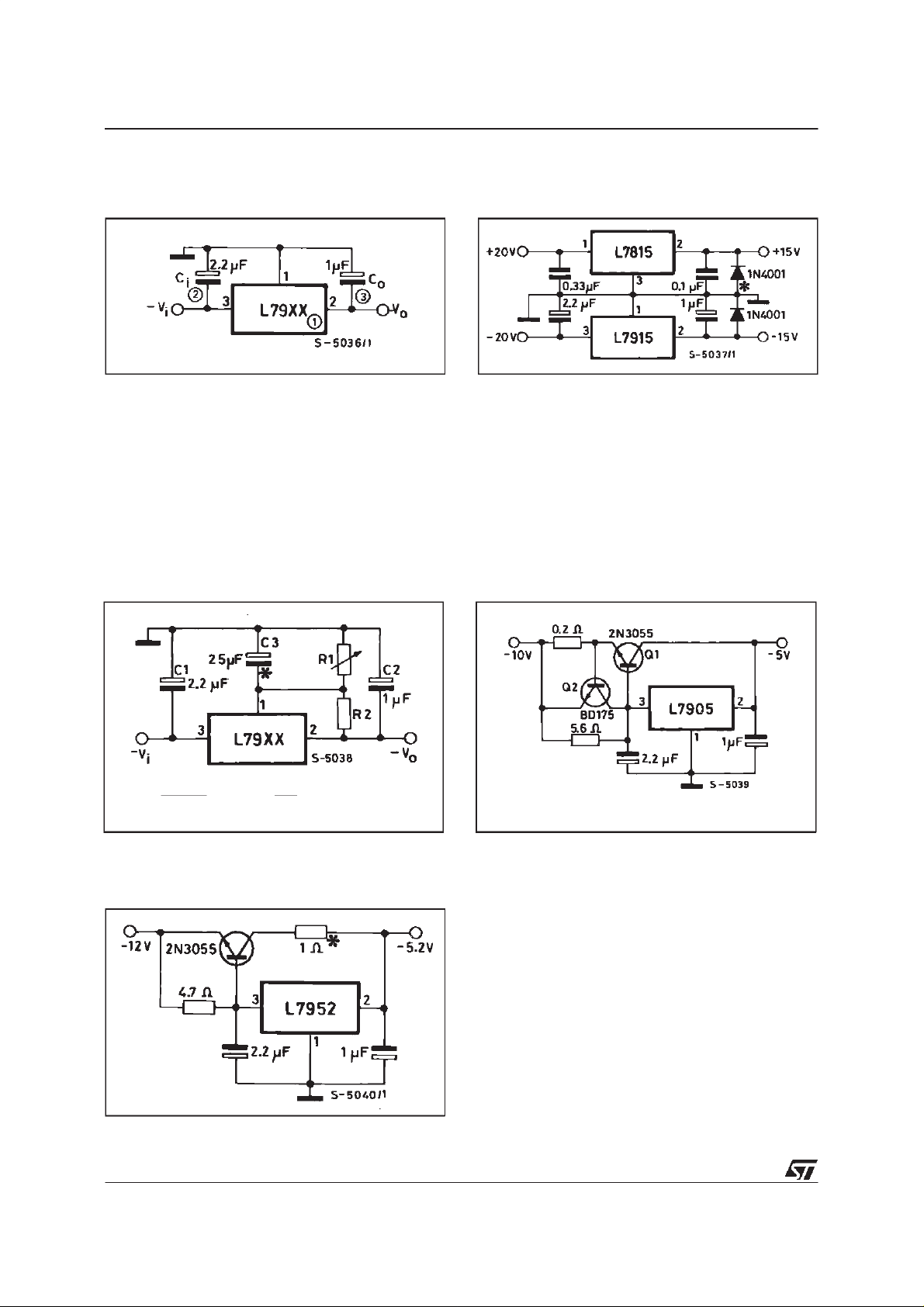
APPLICATIONINFORMATION
Figure1 : Fixed Output Regulator. Figure 2 : Split Power Supply (± 15V/1A).
Notes :
1. To specify an outputvoltage, substitute voltage value for ”XX”.
2. Required for stability. For value given, capacitor must be solid
tantalum. If aluminium electrolitics are used, at least ten times
value should be selected. C
appreciable distance from power supply filter.
3. To improve transient response. If large capacitors are used, a
high current diode from input to output (1N4001 or similar) should
be introduced to protect the device from momentary input short
circuit.
is required if regulator is located an
1
Against potential latch-up problems.
Figure3 : Circuit for Increasing Output Voltage. Figure 4 : High CurrentNegative Regulator
(– 5V/4Awith 5A current limiting).
R
+
R
1
=
V
V
O
XX
2
R
2
V
XX
> 3
I
d
R
2
C3 Optional for improved transient response and ripple rejection.
Figure5 : TypicalECL System Power Supply
(– 5.2V/4A).
Optional dropping resistor to reduce the power dissipated in the
boost transistor.
8/11
Page 9
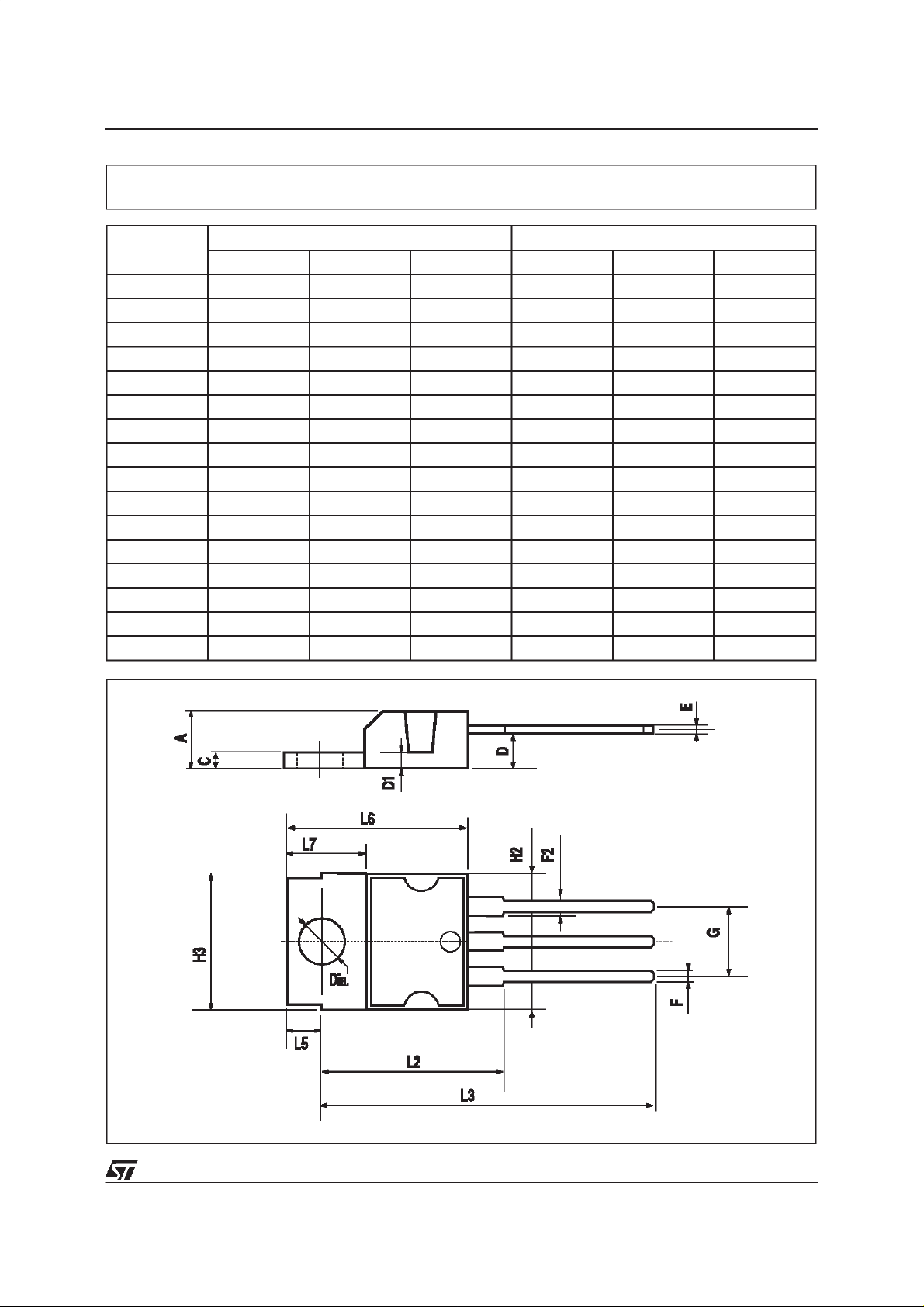
TO-220 MECHANICALDATA
L7900AC
DIM.
MIN. TYP. MAX. MIN. TYP. MAX.
A 4.8 0.189
C 1.37 0.054
D 2.4 2.8 0.094 0.110
D1 1.2 1.35 0.047 0.053
E 0.35 0.55 0.014 0.022
F 0.61 0.94 0.024 0.037
F2 1.15 1.4 0.045 0.055
G 4.95 5.08 5.21 0.195 0.200 0.205
H2 10.4 0.409
H3 10.05 10.4 0.396 0.409
L2 16.2 0.638
L3 26.3 26.7 27.1 1.035 1.051 1.067
L5 2.6 3 0.102 0.118
L6 15.1 15.8 0.594 0.622
L7 6 6.6 0.236 0.260
Dia. 3.65 3.85 0.144 0.152
mm inch
P011D
9/11
Page 10
L7900AC
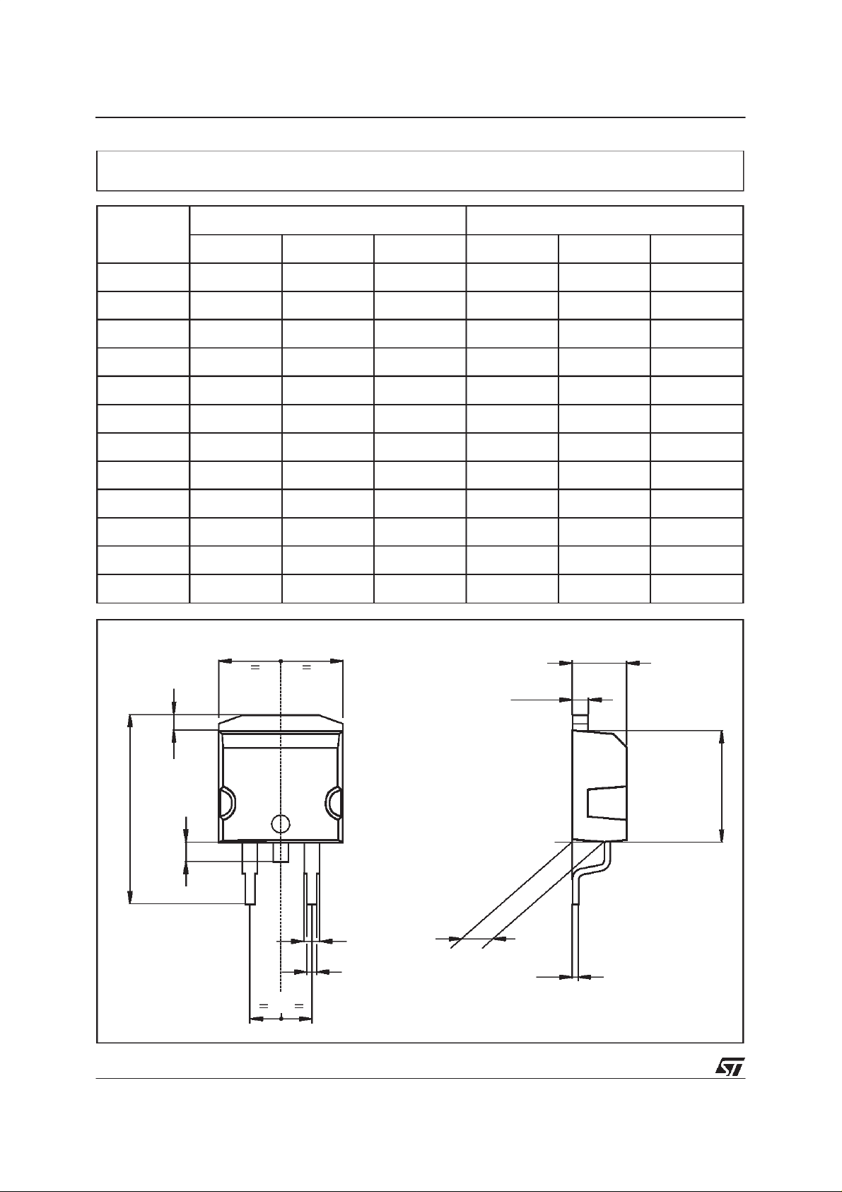
TO-263 (D2PAK) MECHANICAL DATA
DIM.
MIN. TYP. MAX. MIN. TYP. MAX.
A 4.3 4.6 0.169 0.181
A1 2.49 2.69 0.098 0.106
B 0.7 0.93 0.027 0.036
B2 1.25 1.4 0.049 0.055
C 0.45 0.6 0.017 0.023
C2 1.21 1.36 0.047 0.053
D 8.95 9.35 0.352 0.368
E 10 10.28 0.393 0.404
G 4.88 5.28 0.192 0.208
L 15 15.85 0.590 0.624
L2 1.27 1.4 0.050 0.055
L3 1.4 1.75 0.055 0.068
mm inch
E
A
C2
L2
D
L
L3
B2
B
A1
C
G
P011P6/C
10/11
Page 11

L7900AC
Information furnished is believed to beaccurate and reliable. However, STMicroelectronics assumes no responsibility forthe consequences
of use of such information nor for any infringement of patents or other rights of third parties which may result from its use. No license is
granted by implication or otherwise under any patent or patent rights of STMicroelectronics. Specification mentioned in this publication are
subject to change without notice. Thispublication supersedes and replaces allinformation previously supplied. STMicroelectronics products
are not authorized for use as critical components in life support devices or systems without express written approval ofSTMicroelectronics.
The ST logo is a trademark of STMicroelectronics
1998 STMicroelectronics – Printed in Italy – All Rights Reserved
STMicroelectronics GROUP OF COMPANIES
Australia - Brazil - Canada - China -France -Germany - Italy- Japan -Korea -Malaysia - Malta - Morocco - The Netherlands -
Singapore - Spain - Sweden - Switzerland - Taiwan- Thailand - United Kingdom - U.S.A.
.
11/11
 Loading...