

Datasheet L78L15ACUTR, L78L24ACUTR, L78L15ABUTR, L78L12ACUTR, L78L12ABUTR Datasheet (SGS Thomson Microelectronics)
...Page 1

1/24July 2003
■ OUTPUT CURRENT UP TO 100 mA
■ OUTPUT VOLTAGES OF 3.3; 5; 6; 8; 9; 10;
12; 15; 18; 20; 24V
■ THERMAL OVERLOAD PROTECTION
■ SHORT CIRCUIT PROTECTION
■ NO EXTERNAL COMPONENTS A RE
REQUIRED
■ AVAILABLE IN EITHER ±5% (AC) OR ±10%
(C) SELECTION
DESCRIPTION
The L78L00 series of three-terminal positive
regulators employ internal current limiting and
thermal shutdown, making them essen tially
indestructible. If adequate heat-sink is provided,
they can deliverup to 100 mA output current. T hey
are i nte nded as fixed volt age regulators in a wide
range of applications including local or on-card
regulation for elimination of noise and distribution
problems associated with single-poi nt regulation.
In addition, they c an be used with power pass
elements to make high-current voltage regulators.
The L78L00 series used as Zener diode/resistor
combination replacement, offers an effective
output impedanc e improvement of typically t wo
orders of magnitude, along with lower quiescent
current and lower noise.
L78L00
SERIES
POSITIVE VOLTAGE REGULATORS
SCHEMATIC DIAGRAM
TO-92
SOT-89SO-8
Page 2
L78L00 SERIES
2/24
ABSOLUTE MAXIMUM RATINGS
(*) Our SO-8 package used for Voltage Regulators is modified internally to have pins 2, 3, 6 and 7 electrically communed to the die attach
flag. This particular frame decreases the total thermal resistance of the package and increases its ability to dissipate power when a n appropriate area of copper on the printed circuit board is available for heat-sinking. The external dimensions are the same as forthestandard SO-8.
THERMAL DATA
(*) Considering 6 cm2of copper Board heat-sink
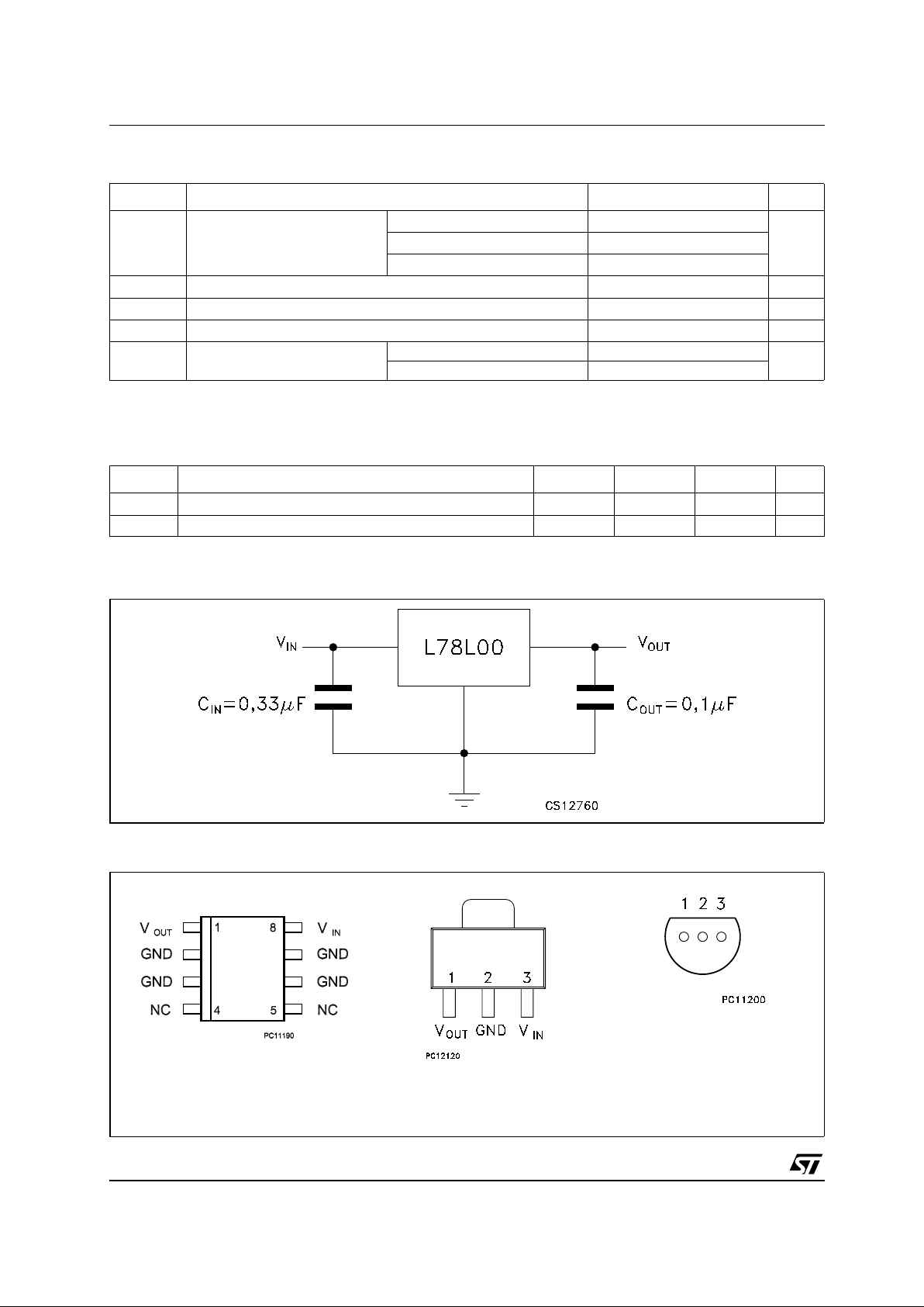
TEST CIRCUITS
CONNECTION DIAGRAM (top view)
Symbol Parameter² Value Unit
V
I
DC Input Voltage VO= 3.3 to 9 V
30
V
V
O
=12to15V
35
V
O
=18to24V
40
I
O
Output Current
100 mA
P
tot
Power Dissipation
Internally Limited (*)
T
stg
Storage Temperature Range
-40 to 150 °C
T
op
OperatingJunctionTemperature
Range
for L78L00C, L78L00AC 0 to 125
°C
for L78L00AB -40 to 125
Symbol Parameter SO-8 TO-92 SOT-89 Unit
R
thj-case
Thermal Resistance Junction-case Max
20 15 °C/W
R
thj-amb
Thermal Resistance Junction-ambient Max
55 (*) 200 °C/W
SOT-89SO-8
BOTTOM VIEW
PIN 1 = V
OUT
PIN 2 = GND
PIN 3 = V
IN
TO-92
Page 3
L78L00 SE RIE S
3/24
ORDERING CODES
(*) Available in Tape & Reel with the suffix "13TR".
(**) Available in Ammopak with the suffix "-AP" or in Tape & Reel with the suffix "TR".
TYPE SO-8 (TUBE)* TO-92 (TUBE)** SOT-89 (T&R) OUTPUT VOLTAGE
L78L33C L78L33CD L78L33CZ 3.3 V
L78L33AC L78L33ACD L78L33ACZ L78L33ACUTR 3.3 V
L78L33AB L78L33ABD L78L33ABZ L78L33ABUTR 3.3 V
L78L05C L78L05CD L78L05CZ 5 V
L78L05AC L78L05ACD L78L05ACZ L78L05ACUTR 5 V
L78L05AB L78L05ABD L78L05ABZ L78L05ABUTR 5 V
L78L06C L78L06CD L78L06CZ 6 V
L78L06AC L78L06ACD L78L06ACZ L78L06ACUTR 6 V
L78L06AB L78L06ABD L78L06ABZ L78L06ABUTR 6 V
L78L08C L78L08CD L78L08CZ 8 V
L78L08AC L78L08ACD L78L08ACZ L78L08ACUTR 8 V
L78L08AB L78L08ABD L78L08ABZ L78L08ABUTR 8 V
L78L09C L78L09CD L78L09CZ 9 V
L78L09AC L78L09ACD L78L09ACZ L78L09ACUTR 9 V
L78L09AB L78L09ABD L78L09ABZ L78L09ABUTR 9 V
L78L10C L78L10CD L78L10CZ 10 V
L78L10AC L78L10ACD L78L10ACZ L78L10ACUTR 10 V
L78L10AB L78L10ABD L78L10ABZ L78L10ABUTR 10 V
L78L12C L78L12CD L78L12CZ 12 V
L78L12AC L78L12ACD L78L12ACZ L78L12ACUTR 12 V
L78L12AB L78L12ABD L78L12ABZ L78L12ABUTR 12 V
L78L15C L78L15CD L78L15CZ 15 V
L78L15AC L78L15ACD L78L15ACZ L78L15ACUTR 15 V
L78L15AB L78L15ABD L78L15ABZ L78L15ABUTR 15 V
L78L18C L78L18CD L78L18CZ 18 V
L78L18AC L78L18ACD L78L18ACZ L78L18ACUTR 18 V
L78L18AB L78L18ABD L78L18ABZ L78L18ABUTR 18 V
L78L20C L78L20CD L78L20CZ 20 V
L78L20AC L78L20ACD L78L20ACZ L78L20ACUTR 20 V
L78L20AB L78L20ABD L78L20ABZ L78L20ABUTR 20 V
L78L24C L78L24CD L78L24CZ 24 V
L78L24AC L78L24ACD L78L24ACZ L78L24ACUTR 24 V
L78L24AB L78L24ABD L78L24ABZ L78L24ABUTR 24 V
Page 4

L78L00 SERIES
4/24
ELECTRICAL CHARACTERISTICS OF L78L33C (refer to the test circuits, TJ= 0 to 125°C, VI=8.3V,
I
O
=40mA,CI=0.33µF,CO= 0.1 µ F unless otherwise specified)
ELECTRICAL CHARACTERISTICS OF L78L05C (refer to the test circuits, T
J
= 0 to 125°C, VI=10V,
I
O
=40mA,CI=0.33µF,CO= 0.1 µ F unless otherwise specified).
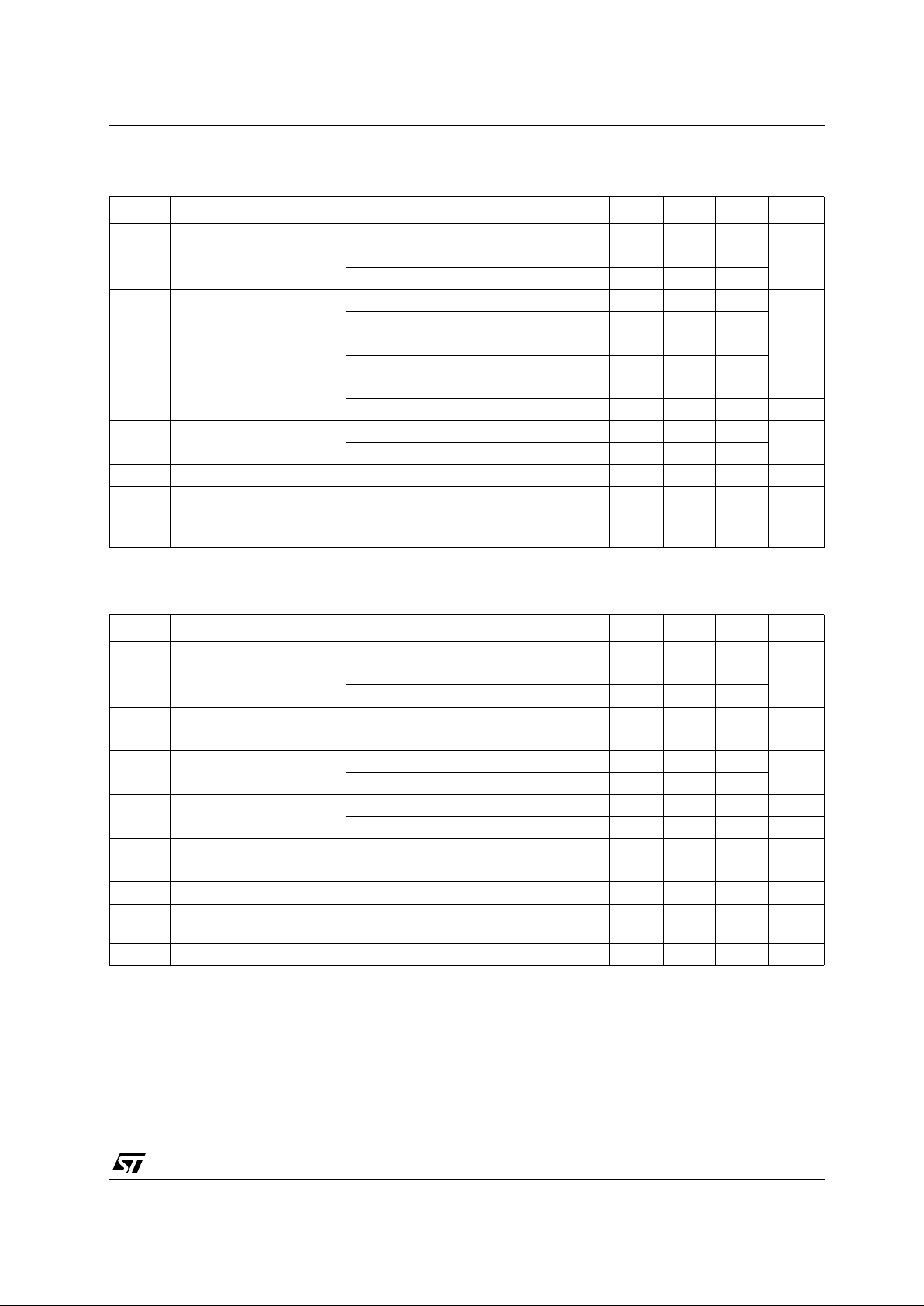
Symbol Parameter Test Conditions Min. Typ. Max. Unit
V
O
Output Voltage TJ= 25°C 3.036 3.3 3.564 V
V
O
Output Voltage IO= 1 to 40 mA VI= 5.3 to 20 V 2.97 3.63 V
I
O
= 1 to 70 mA VI= 8.3 V 2.97 3.63
∆V
O
Line Regulation VI= 5.3 to 20 V TJ= 25°C 150 mV
V
I
= 6.3 to 20 V TJ= 25°C 100
∆V
O
Load Regulation IO= 1 to 100 mA TJ= 25°C 60 mV
I
O
=1to40mA TJ= 25°C 30
I
d
Quiescent Current TJ= 25°C 6 mA
T
J
= 125°C 5.5 mA
∆I
d
Quiescent Current Change IO=1to40mA 0.2 mA
V
I
= 6.3 to 20 V 1.5
eN Output Noise Voltage B =10Hz to 100KHz T
J
= 25°C 40 µV
SVR Supply Voltage Rejection V
I
= 6.3 to 16.3 V f = 120Hz
I
O
=40mA TJ= 25°C
41 49 dB
V
d
Dropout Voltage 1.7 V
Symbol Parameter Test Conditions Min. Typ. Max. Unit
V
O
Output Voltage TJ= 25°C 4.6 5 5.4 V
V
O
Output Voltage IO= 1 to 40 mA VI=7 to 20 V 4.5 5.5 V
I
O
= 1 to 70 mA VI= 10 V 4.5 5.5
∆V
O
Line Regulation VI= 8.5 to 20 V TJ= 25°C 200 mV
V
I
=9to20V TJ= 25°C 150
∆V
O
Load Regulation IO= 1 to 100 mA TJ= 25°C 60 mV
I
O
=1to40mA TJ= 25°C 30
I
d
Quiescent Current TJ= 25°C 6 mA
T
J
= 125°C 5.5 mA
∆I
d
Quiescent Current Change IO=1to40mA 0.2 mA
V
I
= 8 to 20 V 1.5
eN Output Noise Voltage B =10Hz to 100KHz T
J
= 25°C 40 µV
SVR Supply Voltage Rejection V
I
= 9 to 20 V f = 120Hz
I
O
=40mA TJ= 25°C
40 49 dB
V
d
Dropout Voltage 1.7 V
Page 5
L78L00 SE RIE S
5/24
ELECTRICAL CHARACTERISTICS OF L78L06C (refer to the test circuits, TJ= 0 to 125°C, VI=12V,
I
O
=40mA,CI=0.33µF,CO= 0.1 µ F unless otherwise specified).
ELECTRICAL CHARACTERISTICS OF L78L08C (refer to the test circuits, T
J
= 0 to 125°C, VI=14V,
I
O
=40mA,CI=0.33µF,CO= 0.1 µ F unless otherwise specified).
Symbol Parameter Test Conditions Min. Typ. Max. Unit
V
O
Output Voltage TJ= 25°C 5.52 6 6.48 V
V
O
Output Voltage IO= 1 to 40 mA VI=8.5 to 20 V 5.4 6.6 V
I
O
= 1 to 70 mA VI= 12 V 5.4 6.6
∆V
O
Line Regulation VI= 8.5 to 20 V TJ= 25°C 200 mV
V
I
=9to20V TJ= 25°C 150
∆V
O
Load Regulation IO= 1 to 100 mA TJ= 25°C 60 mV
I
O
=1to40mA TJ= 25°C 30
I
d
Quiescent Current TJ= 25°C 6 mA
T
J
= 125°C 5.5 mA
∆I
d
Quiescent Current Change IO=1to40mA 0.2 mA
V
I
= 8 to 20 V 1.5
eN Output Noise Voltage B =10Hz to 100KHz T
J
= 25°C 50 µV
SVR Supply Voltage Rejection V
I
= 9 to 20 V f = 120Hz
I
O
=40mA TJ= 25°C
38 46 dB
V
d
Dropout Voltage 1.7 V
Symbol Parameter Test Conditions Min. Typ. Max. Unit
V
O
Output Voltage TJ= 25°C 7.36 8 8.64 V
V
O
Output Voltage IO= 1 to 40 mA VI=10.5 to 23 V 7.2 8.8 V
I
O
= 1 to 70 mA VI= 14 V 7.2 8.8
∆V
O
Line Regulation VI= 10.5 to 23 V TJ= 25°C 200 mV
V
I
=11to23V TJ= 25°C 150
∆V
O
Load Regulation IO= 1 to 100 mA TJ= 25°C 80 mV
I
O
=1to40mA TJ= 25°C 40
I
d
Quiescent Current TJ= 25°C 6 mA
T
J
= 125°C 5.5 mA
∆I
d
Quiescent Current Change IO=1to40mA 0.2 mA
V
I
=11to23V 1.5
eN Output Noise Voltage B =10Hz to 100KHz T
J
= 25°C 60 µV
SVR Supply Voltage Rejection V
I
= 12 to 23 V f = 120Hz
I
O
=40mA TJ= 25°C
36 45 dB
V
d
Dropout Voltage 1.7 V
Page 6
L78L00 SERIES
6/24
ELECTRICAL CHARACTERISTICS OF L78L09C (refer to the test circuits, TJ= 0 to 125°C, VI=15V,
I
O
=40mA,CI=0.33µF,CO= 0.1 µ F unless otherwise specified).
ELECTRICAL CHARACTERISTICS OF L78L10C (refer to the test circuits, T
J
= 0 to 125°C, VI=16V,
I
O
=40mA,CI=0.33µF,CO= 0.1 µ F unless otherwise specified).
Symbol Parameter Test Conditions Min. Typ. Max. Unit
V
O
Output Voltage TJ= 25°C 8.28 9 9.72 V
V
O
Output Voltage IO= 1 to 40 mA VI=11.5 to 23 V 8.1 9.9 V
I
O
= 1 to 70 mA VI= 15 V 8.1 9.9
∆V
O
Line Regulation VI= 11.5 to 23 V TJ= 25°C 250 mV
V
I
=12to23V TJ= 25°C 200
∆V
O
Load Regulation IO= 1 to 100 mA TJ= 25°C 80 mV
I
O
=1to40mA TJ= 25°C 40
I
d
Quiescent Current TJ= 25°C 6 mA
T
J
= 125°C 5.5 mA
∆I
d
Quiescent Current Change IO=1to40mA 0.2 mA
V
I
=12to23V 1.5
eN Output Noise Voltage B =10Hz to 100KHz T
J
= 25°C 70 µV
SVR Supply Voltage Rejection V
I
= 12 to 23 V f = 120Hz
I
O
=40mA TJ= 25°C
36 44 dB
V
d
Dropout Voltage 1.7 V
Symbol Parameter Test Conditions Min. Typ. Max. Unit
V
O
Output Voltage TJ= 25°C 9.2 10 10.8 V
V
O
Output Voltage IO= 1 to 40 mA VI=12.5 to 23 V 9 11 V
I
O
= 1 to 70 mA VI=16V 9 11
∆V
O
Line Regulation VI= 12.5 to 23 V TJ= 25°C 230 mV
V
I
=13to23V TJ= 25°C 170
∆V
O
Load Regulation IO= 1 to 100 mA TJ= 25°C 80 mV
I
O
=1to40mA TJ= 25°C 40
I
d
Quiescent Current TJ= 25°C 6 mA
T
J
= 125°C 5.5 mA
∆I
d
Quiescent Current Change IO=1to40mA 0.1 mA
V
I
=13to23V 1.5
eN Output Noise Voltage B =10Hz to 100KHz T
J
= 25°C 60 µV
SVR Supply Voltage Rejection V
I
= 14 to 23 V f = 120Hz
I
O
=40mA TJ= 25°C
37 45 dB
V
d
Dropout Voltage 1.7 V
Page 7
L78L00 SE RIE S
7/24
ELECTRICAL CHARACTERISTICS OF L78L12C (refer to the test circuits, TJ= 0 to 125°C, VI=19V,
I
O
=40mA,CI=0.33µF,CO= 0.1 µ F unless otherwise specified).
ELECTRICAL CHARACTERISTICS OF L78L15C (refer to the test circuits, T
J
= 0 to 125°C, VI=23V,
I
O
=40mA,CI=0.33µF,CO= 0.1 µ F unless otherwise specified).
Symbol Parameter Test Conditions Min. Typ. Max. Unit
V
O
Output Voltage TJ= 25°C 11.1 12 12.9 V
V
O
Output Voltage IO= 1 to 40 mA VI=14.5 to 27 V 10.8 13.2 V
I
O
= 1 to 70 mA VI= 19 V 10.8 13.2
∆V
O
Line Regulation VI= 14.5 to 27 V TJ= 25°C 250 mV
V
I
=16to27V TJ= 25°C 200
∆V
O
Load Regulation IO= 1 to 100 mA TJ= 25°C 100 mV
I
O
=1to40mA TJ= 25°C 50
I
d
Quiescent Current TJ= 25°C 6.5 mA
T
J
= 125°C 6 mA
∆I
d
Quiescent Current Change IO=1to40mA 0.2 mA
V
I
=16to27V 1.5
eN Output Noise Voltage B =10Hz to 100KHz T
J
= 25°C 80 µV
SVR Supply Voltage Rejection V
I
= 15 to 25 V f = 120Hz
I
O
=40mA TJ= 25°C
36 42 dB
V
d
Dropout Voltage 1.7 V
Symbol Parameter Test Conditions Min. Typ. Max. Unit
V
O
Output Voltage TJ= 25°C 13.8 15 16.2 V
V
O
Output Voltage IO= 1 to 40 mA VI=17.5 to 30 V 13.5 16.5 V
I
O
= 1 to 70 mA VI= 23 V 13.5 16.5
∆V
O
Line Regulation VI= 17.5 to 30 V TJ= 25°C 300 mV
V
I
=20to30V TJ= 25°C 250
∆V
O
Load Regulation IO= 1 to 100 mA TJ= 25°C 150 mV
I
O
=1to40mA TJ= 25°C 75
I
d
Quiescent Current TJ= 25°C 6.5 mA
T
J
= 125°C 6 mA
∆I
d
Quiescent Current Change IO=1to40mA 0.2 mA
V
I
=20to30V 1.5
eN Output Noise Voltage B =10Hz to 100KHz T
J
= 25°C 90 µV
SVR Supply Voltage Rejection V
I
= 18.5 to 28.5 V f = 120Hz
I
O
=40mA TJ= 25°C
33 39 dB
V
d
Dropout Voltage 1.7 V
Page 8

L78L00 SERIES
8/24
ELECTRICAL CHARACTERISTICS OF L78L18C (refer to the test circuits, TJ= 0 to 125°C, VI=27V,
I
O
=40mA,CI=0.33µF,CO= 0.1 µ F unless otherwise specified).
ELECTRICAL CHARACTERISTICS OF L78L20C (refer to the test circuits, T
J
= 0 to 125°C, VI=29V,
I
O
=40mA,CI=0.33µF,CO= 0.1 µ F unless otherwise specified)
Symbol Parameter Test Conditions Min. Typ. Max. Unit
V
O
Output Voltage TJ= 25°C 16.6 18 19.4 V
V
O
Output Voltage IO= 1 to 40 mA VI=22to33V 16.2 19.8 V
I
O
= 1 to 70 mA VI= 27 V 16.2 19.8
∆V
O
Line Regulation VI=22to33V TJ= 25°C 320 mV
V
I
=22to33V TJ= 25°C 270
∆V
O
Load Regulation IO= 1 to 100 mA TJ= 25°C 170 mV
I
O
=1to40mA TJ= 25°C 85
I
d
Quiescent Current TJ= 25°C 6.5 mA
T
J
= 125°C 6 mA
∆I
d
Quiescent Current Change IO=1to40mA 0.2 mA
V
I
=23to33V 1.5
eN Output Noise Voltage B =10Hz to 100KHz T
J
= 25°C 120 µV
SVR Supply Voltage Rejection V
I
= 23 to 33 V f = 120Hz
I
O
=40mA TJ= 25°C
32 38 dB
V
d
Dropout Voltage 1.7 V
Symbol Parameter Test Conditions Min. Typ. Max. Unit
V
O
Output Voltage TJ= 25°C 18.4 20 21.6 V
V
O
Output Voltage IO= 1 to 40 mA VI=24to33V 18 22 V
I
O
= 1 to 70 mA VI=29V 18 22
∆V
O
Line Regulation VI= 22.5 to 34 V TJ= 25°C 330 mV
V
I
=24to34V TJ= 25°C 280
∆V
O
Load Regulation IO= 1 to 100 mA TJ= 25°C 180 mV
I
O
=1to40mA TJ= 25°C 90
I
d
Quiescent Current TJ= 25°C 6.5 mA
T
J
= 125°C 6 mA
∆I
d
Quiescent Current Change IO=1to40mA 0.2 mA
V
I
=25to33V 1.5
eN Output Noise Voltage B =10Hz to 100KHz T
J
= 25°C 120 µV
SVR Supply Voltage Rejection V
I
= 25 to 35 V f = 120Hz
I
O
=40mA TJ= 25°C
31 38 dB
V
d
Dropout Voltage 1.7 V
Page 9

L78L00 SE RIE S
9/24
ELECTRICAL CHARACTERISTICS OF L78L24C (refer to the test circuits, TJ= 0 to 125°C, VI=33V,
I
O
=40mA,CI=0.33µF,CO= 0.1 µ F unless otherwise specified).
ELECTRICAL CHARACTERISTICS OF L78L33AB AND L78L33AC
(refer to the test circuits, V
I
=8.3V,IO=40mA,CI=0.33µF,CO=0.1µF,
T
J
= 0 to 125°C for L78L33AC, TJ= -40 to 125°C for L78L33AB, unless otherwise specif ied)
Symbol Parameter Test Conditions Min. Typ. Max. Unit
V
O
Output Voltage TJ= 25°C 22.1 24 25.9 V
V
O
Output Voltage IO= 1 to 40 mA VI=27to38V 21.6 26.4 V
I
O
= 1 to 70 mA VI= 33 V 21.6 26.4
∆V
O
Line Regulation VI=27to38V TJ= 25°C 350 mV
V
I
=28to38V TJ= 25°C 300
∆V
O
Load Regulation IO= 1 to 100 mA TJ= 25°C 200 mV
I
O
=1to40mA TJ= 25°C 100
I
d
Quiescent Current TJ= 25°C 6.5 mA
T
J
= 125°C 6 mA
∆I
d
Quiescent Current Change IO=1to40mA 0.2 mA
V
I
=28to38V 1.5
eN Output Noise Voltage B =10Hz to 100KHz T
J
= 25°C 200 µV
SVR Supply Voltage Rejection V
I
= 29 to 35 V f = 120Hz
I
O
=40mA TJ= 25°C
30 37 dB
V
d
Dropout Voltage 1.7 V
Symbol Parameter Test Conditions Min. Typ. Max. Unit
V
O
Output Voltage TJ= 25°C 3.168 3.3 3.432 V
V
O
Output Voltage IO= 1 to 40 mA VI= 5.3 to 20 V 3.135 3.465 V
I
O
= 1 to 70 mA VI= 8.3 V 3.135 3.465
∆V
O
Line Regulation VI= 5.3 to 20 V TJ= 25°C 150 mV
V
I
= 6.3 to 20 V TJ= 25°C 100
∆V
O
Load Regulation IO= 1 to 100 mA TJ= 25°C 60 mV
I
O
=1to40mA TJ= 25°C 30
I
d
Quiescent Current TJ= 25°C 6 mA
T
J
= 125°C 5.5 mA
∆I
d
Quiescent Current Change IO=1to40mA 0.1 mA
V
I
= 6.3 to 20 V 1.5
eN Output Noise Voltage B =10Hz to 100KHz T
J
= 25°C 40 µV
SVR Supply Voltage Rejection V
I
= 6.3 to 16.3 V f = 120Hz
I
O
=40mA TJ= 25°C
41 49 dB
V
d
Dropout Voltage 1.7 V
Page 10

L78L00 SERIES
10/24
ELECTRICAL CHARACTERISTICS OF L78L05AB AND L78L05AC
(refer to the test circuits, V
I
= 10V, IO=40mA,CI=0.33µF,CO=0.1µF,
T
J
= 0 to 125°C for L78L05AC, TJ= -40 to 125°C for L78L05AB, unless otherwise specif ied)
ELECTRICAL CHARACTERISTICS OF L78L06AB AND L78L06AC
(refer to the test circuits, V
I
= 12V, IO=40mA,CI=0.33µF,CO=0.1µF,
T
J
= 0 to 125°C for L78L06AC, TJ= -40 to 125°C for L78L06AB, unless otherwise specif ied)
Symbol Parameter Test Conditions Min. Typ. Max. Unit
V
O
Output Voltage TJ= 25°C 4.8 5 5.2 V
V
O
Output Voltage IO= 1 to 40 mA VI= 7 to 20 V 4.75 5.25 V
I
O
= 1 to 70 mA VI= 10 V 4.75 5.25
∆V
O
Line Regulation VI=7to20V TJ= 25°C 150 mV
V
I
=8to20V TJ= 25°C 100
∆V
O
Load Regulation IO= 1 to 100 mA TJ= 25°C 60 mV
I
O
=1to40mA TJ= 25°C 30
I
d
Quiescent Current TJ= 25°C 6 mA
T
J
= 125°C 5.5 mA
∆I
d
Quiescent Current Change IO=1to40mA 0.1 mA
V
I
= 8 to 20 V 1.5
eN Output Noise Voltage B =10Hz to 100KHz T
J
= 25°C 40 µV
SVR Supply Voltage Rejection V
I
= 8 to 18 V f = 120Hz
I
O
=40mA TJ= 25°C
41 49 dB
V
d
Dropout Voltage 1.7 V
Symbol Parameter Test Conditions Min. Typ. Max. Unit
V
O
Output Voltage TJ= 25°C 5.76 6 6.24 V
V
O
Output Voltage IO= 1 to 40 mA VI= 8.5 to 20 V 5.7 6.3 V
I
O
= 1 to 70 mA VI= 12 V 5.7 6.3
∆V
O
Line Regulation VI= 8.5 to 20 V TJ= 25°C 150 mV
V
I
=9to20V TJ= 25°C 100
∆V
O
Load Regulation IO= 1 to 100 mA TJ= 25°C 60 mV
I
O
=1to40mA TJ= 25°C 30
I
d
Quiescent Current TJ= 25°C 6 mA
T
J
= 125°C 5.5 mA
∆I
d
Quiescent Current Change IO=1to40mA 0.1 mA
V
I
= 9 to 20 V 1.5
eN Output Noise Voltage B =10Hz to 100KHz T
J
= 25°C 50 µV
SVR Supply Voltage Rejection V
I
= 9 to 20 V f = 120Hz
I
O
=40mA TJ= 25°C
39 46 dB
V
d
Dropout Voltage 1.7 V
Page 11

L78L00 SE RIE S
11/24
ELECTRICAL CHARACTERISTICS OF L78L08AB AND L78L08AC
(refer to the test circuits, V
I
= 14V, IO=40mA,CI=0.33µF,CO=0.1µF,
T
J
= 0 to 125°C for L78L08AC, TJ= -40 to 125°C for L78L08AB, unless otherwise specif ied)
ELECTRICAL CHARACTERISTICS OF L78L09AB AND L78L09AC
(refer to the test circuits, V
I
= 15V, IO=40mA,CI=0.33µF,CO=0.1µF,
T
J
= 0 to 125°C for L78L09AC, TJ= -40 to 125°C for L78L09AB, unless otherwise specif ied)
Symbol Parameter Test Conditions Min. Typ. Max. Unit
V
O
Output Voltage TJ= 25°C 7.68 8 8.32 V
V
O
Output Voltage IO= 1 to 40 mA VI= 10.5 to 23 V 7.6 8.4 V
I
O
= 1 to 70 mA VI= 14 V 7.6 8.4
∆V
O
Line Regulation VI= 10.5 to 23 V TJ= 25°C 175 mV
V
I
=11to23V TJ= 25°C 125
∆V
O
Load Regulation IO= 1 to 100 mA TJ= 25°C 80 mV
I
O
=1to40mA TJ= 25°C 40
I
d
Quiescent Current TJ= 25°C 6 mA
T
J
= 125°C 5.5 mA
∆I
d
Quiescent Current Change IO=1to40mA 0.1 mA
V
I
=11to23V 1.5
eN Output Noise Voltage B =10Hz to 100KHz T
J
= 25°C 60 µV
SVR Supply Voltage Rejection V
I
= 12 to 23 V f = 120Hz
I
O
=40mA TJ= 25°C
37 45 dB
V
d
Dropout Voltage 1.7 V
Symbol Parameter Test Conditions Min. Typ. Max. Unit
V
O
Output Voltage TJ= 25°C 8.64 9 9.36 V
V
O
Output Voltage IO= 1 to 40 mA VI= 11.5 to 23 V 8.55 9.45 V
I
O
= 1 to 70 mA VI= 15 V 8.55 9.45
∆V
O
Line Regulation VI= 11.5 to 23 V TJ= 25°C 225 mV
V
I
=12to23V TJ= 25°C 150
∆V
O
Load Regulation IO= 1 to 100 mA TJ= 25°C 80 mV
I
O
=1to40mA TJ= 25°C 40
I
d
Quiescent Current TJ= 25°C 6 mA
T
J
= 125°C 5.5 mA
∆I
d
Quiescent Current Change IO=1to40mA 0.1 mA
V
I
=12to23V 1.5
eN Output Noise Voltage B =10Hz to 100KHz T
J
= 25°C 70 µV
SVR Supply Voltage Rejection V
I
= 12 to 23 V f = 120Hz
I
O
=40mA TJ= 25°C
37 44 dB
V
d
Dropout Voltage 1.7 V
Page 12

L78L00 SERIES
12/24
ELECTRICAL CHARACTERISTICS OF L78L10AB AND L78L10AC
(refer to the test circuits, V
I
= 16V, IO=40mA,CI=0.33µF,CO=0.1µF,
T
J
= 0 to 125°C for L78L10AC, TJ= -40 to 125°C for L78L10AB, unless otherwise specif ied)
ELECTRICAL CHARACTERISTICS OF L78L12AB AND L78L12AC
(refer to the test circuits, V
I
= 19V, IO=40mA,CI=0.33µF,CO=0.1µF,
T
J
= 0 to 125°C for L78L12AC, TJ= -40 to 125°C for L78L12AB, unless otherwise specif ied)
Symbol Parameter Test Conditions Min. Typ. Max. Unit
V
O
Output Voltage TJ= 25°C 9.6 10 10.4 V
V
O
Output Voltage IO= 1 to 40 mA VI=12.5 to 23 V 9.5 10.5 V
I
O
= 1 to 70 mA VI= 16 V 9.5 10.5
∆V
O
Line Regulation VI= 12.5 to 23 V TJ= 25°C 230 mV
V
I
=13to23V TJ= 25°C 170
∆V
O
Load Regulation IO= 1 to 100 mA TJ= 25°C 80 mV
I
O
=1to40mA TJ= 25°C 40
I
d
Quiescent Current TJ= 25°C 6 mA
T
J
= 125°C 5.5 mA
∆I
d
Quiescent Current Change IO=1to40mA 0.1 mA
V
I
=13to23V 1.5
eN Output Noise Voltage B =10Hz to 100KHz T
J
= 25°C 60 µV
SVR Supply Voltage Rejection V
I
= 14 to 23 V f = 120Hz
I
O
=40mA TJ= 25°C
37 45 dB
V
d
Dropout Voltage 1.7 V
Symbol Parameter Test Conditions Min. Typ. Max. Unit
V
O
Output Voltage TJ= 25°C 11.5 12 12.5 V
V
O
Output Voltage IO= 1 to 40 mA VI= 14.5 to 27 V 11.4 12.6 V
I
O
= 1 to 70 mA VI= 19 V 11.4 12.6
∆V
O
Line Regulation VI= 14.5 to 27 V TJ= 25°C 250 mV
V
I
=16to27V TJ= 25°C 200
∆V
O
Load Regulation IO= 1 to 100 mA TJ= 25°C 100 mV
I
O
=1to40mA TJ= 25°C 50
I
d
Quiescent Current TJ= 25°C 6.5 mA
T
J
= 125°C 6 mA
∆I
d
Quiescent Current Change IO=1to40mA 0.1 mA
V
I
=16to27V 1.5
eN Output Noise Voltage B =10Hz to 100KHz T
J
= 25°C 80 µV
SVR Supply Voltage Rejection V
I
= 15 to 25 V f = 120Hz
I
O
=40mA TJ= 25°C
37 42 dB
V
d
Dropout Voltage 1.7 V
Page 13

L78L00 SE RIE S
13/24
ELECTRICAL CHARACTERISTICS OF L78L15AB AND L78L15AC
(refer to the test circuits, V
I
= 19V, IO=40mA,CI=0.33µF,CO=0.1µF,
T
J
= 0 to 125°C for L78L15AC, TJ= -40 to 125°C for L78L15AB, unless otherwise specif ied)
ELECTRICAL CHARACTERISTICS OF L78L18AB AND L78L18AC
(refer to the test circuits, V
I
= 27V, IO=40mA,CI=0.33µF,CO=0.1µF,
T
J
= 0 to 125°C for L78L18AC, TJ= -40 to 125°C for L78L18AB, unless otherwise specif ied)
Symbol Parameter Test Conditions Min. Typ. Max. Unit
V
O
Output Voltage TJ= 25°C 14.4 15 15.6 V
V
O
Output Voltage IO= 1 to 40 mA VI= 17.5 to 30 V 14.25 15.75 V
I
O
= 1 to 70 mA VI= 23 V 14.25 15.75
∆V
O
Line Regulation VI= 17.5 to 30 V TJ= 25°C 300 mV
V
I
=20to30V TJ= 25°C 250
∆V
O
Load Regulation IO= 1 to 100 mA TJ= 25°C 150 mV
I
O
=1to40mA TJ= 25°C 75
I
d
Quiescent Current TJ= 25°C 6.5 mA
T
J
= 125°C 6 mA
∆I
d
Quiescent Current Change IO=1to40mA 0.1 mA
V
I
=20to30V 1.5
eN Output Noise Voltage B =10Hz to 100KHz T
J
= 25°C 90 µV
SVR Supply Voltage Rejection V
I
= 18.5 to 28.5 V f = 120Hz
I
O
=40mA TJ= 25°C
34 39 dB
V
d
Dropout Voltage 1.7 V
Symbol Parameter Test Conditions Min. Typ. Max. Unit
V
O
Output Voltage TJ= 25°C 17.3 18 18.7 V
V
O
Output Voltage IO= 1 to 40 mA VI=22to33V 17.1 18.9 V
I
O
= 1 to 70 mA VI= 27 V 17.1 18.9
∆V
O
Line Regulation VI=22to33V TJ= 25°C 320 mV
V
I
=22to33V TJ= 25°C 270
∆V
O
Load Regulation IO= 1 to 100 mA TJ= 25°C 170 mV
I
O
=1to40mA TJ= 25°C 85
I
d
Quiescent Current TJ= 25°C 6.5 mA
T
J
= 125°C 6 mA
∆I
d
Quiescent Current Change IO=1to40mA 0.1 mA
V
I
=23to33V 1.5
eN Output Noise Voltage B =10Hz to 100KHz T
J
= 25°C 120 µV
SVR Supply Voltage Rejection V
I
= 23 to 33 V f = 120Hz
I
O
=40mA TJ= 25°C
33 38 dB
V
d
Dropout Voltage 1.7 V
Page 14

L78L00 SERIES
14/24
ELECTRICAL CHARACTERISTICS OF L78L20AB AND L78L20AC
(refer to the test circuits, V
I
= 29V, IO=40mA,CI=0.33µF,CO=0.1µF,
T
J
= 0 to 125°C for L78L20AC, TJ= -40 to 125°C for L78L20AB, unless otherwise specif ied)
ELECTRICAL CHARACTERISTICS OF L78L24AB AND L78L24AC
(refer to the test circuits, V
I
= 27V, IO=40mA,CI=0.33µF,CO=0.1µF,
T
J
= 0 to 125°C for L78L24AC, TJ= -40 to 125°C for L78L24AB, unless otherwise specif ied)
Symbol Parameter Test Conditions Min. Typ. Max. Unit
V
O
Output Voltage TJ= 25°C 19.2 20 20.8 V
V
O
Output Voltage IO= 1 to 40 mA VI=24to33V 19 21 V
I
O
= 1 to 70 mA VI=29V 19 21
∆V
O
Line Regulation VI= 22.5 to 34 V TJ= 25°C 330 mV
V
I
=24to34V TJ= 25°C 280
∆V
O
Load Regulation IO= 1 to 100 mA TJ= 25°C 180 mV
I
O
=1to40mA TJ= 25°C 90
I
d
Quiescent Current TJ= 25°C 6.5 mA
T
J
= 125°C 6 mA
∆I
d
Quiescent Current Change IO=1to40mA 0.1 mA
V
I
=25to33V 1.5
eN Output Noise Voltage B =10Hz to 100KHz T
J
= 25°C 120 µV
SVR Supply Voltage Rejection V
I
= 25 to 35 V f = 120Hz
I
O
=40mA TJ= 25°C
32 38 dB
V
d
Dropout Voltage 1.7 V
Symbol Parameter Test Conditions Min. Typ. Max. Unit
V
O
Output Voltage TJ=25°C 232425 V
V
O
Output Voltage IO= 1 to 40 mA VI=27to38V 22.8 25.2 V
I
O
= 1 to 70 mA VI= 33 V 22.8 25.2
∆V
O
Line Regulation VI=27to38V TJ= 25°C 350 mV
V
I
=28to38V TJ= 25°C 300
∆V
O
Load Regulation IO= 1 to 100 mA TJ= 25°C 200 mV
I
O
=1to40mA TJ= 25°C 100
I
d
Quiescent Current TJ= 25°C 6.5 mA
T
J
= 125°C 6 mA
∆I
d
Quiescent Current Change IO=1to40mA 0.1 mA
V
I
=28to38V 1.5
eN Output Noise Voltage B =10Hz to 100KHz T
J
= 25°C 200 µV
SVR Supply Voltage Rejection V
I
= 23 to 33 V f = 120Hz
I
O
=40mA TJ= 25°C
31 37 dB
V
d
Dropout Voltage 1.7 V
Page 15

L78L00 SE RIE S
15/24
Figure1 : L78L05/12 Output Voltage vs Am bient
Temperature
Figure2 : L78L05/12/24 Load Characteristics
Figure3 : L78L05/12/24 Thermal Shutdown
Figure4 : L78L05/12 Quiescent Current vs
Output Current
Figure5 : L78L05 Qu iesc ent Current vs Input
Voltage
Figure6 : L78L05/12/24 Out put Characteristics
Page 16

L78L00 SERIES
16/24
Figure7 : L78L05/12/24 Rippl e Rejection
Figure8 : L78L05 Dropout Characteristics
Figure9 : L78L00 Series Short Circuit Output
Current
Page 17

L78L00 SE RIE S
17/24
TYPICAL APPLICATIONS
Table10:High Output Current Short Circuit Protected
Figure11 : Edit Boost Circuit
Figure12 : Current Regulator
Page 18

L78L00 SERIES
18/24
Figure13 : Adjustable Output Regulator
Page 19

L78L00 SE RIE S
19/24
DIM.
mm. inch
MIN. TYP MAX. MIN. TYP. MAX.
A 1.35 1.75 0.053 0.069
A1 0.10 0.25 0.04 0.010
A2 1.10 1.65 0.043 0.065
B 0.33 0.51 0.013 0.020
C 0.19 0.25 0.007 0.010
D 4.80 5.00 0.189 0.197
E 3.80 4.00 0.150 0.157
e 1.27 0.050
H 5.80 6.20 0.228 0.244
h 0.25 0.50 0.010 0.020
L 0.40 1.27 0.016 0.050
k ˚ (max.)
ddd 0.1 0.04
SO-8 MECHANICAL DATA
0016023/C
8
Page 20

L78L00 SERIES
20/24
DIM.
mm. mils
MIN. TYP MAX. MIN. TYP. MAX.
A 1.4 1.6 55.1 63.0
B 0.44 0.56 17.3 22.0
B1 0.36 0.48 14.2 18.9
C 0.35 0.44 13.8 17.3
C1 0.35 0.44 13.8 17.3
D 4.4 4.6 173.2 181.1
D1 1.62 1.83 63.8 72.0
E 2.29 2.6 90.2 102.4
e 1.42 1.57 55.9 61.8
e1 2.92 3.07 115.0 120.9
H 3.94 4.25 155.1 167.3
L 0.89 1.2 35.0 47.2
SOT-89 MECHANICAL DATA
P025H
Page 21

L78L00 SE RIE S
21/24
DIM.
mm. mils
MIN. TYP MAX. MIN. TYP. MAX.
A 4.32 4.95 170.1 194.9
b 0.36 0.51 14.2 20.1
D 4.45 4.95 175.2 194.9
E 3.30 3.94 129.9 155.1
e 2.41 2.67 94.9 105.1
e1 1.14 1.40 44.9 55.1
L 12.7 15.49 500.0 609.8
R 2.16 2.41 85.0 94.9
S1 0.92 1.52 36.2 59.8
W 0.41 0.56 16.1 22.0
TO-92 MECHANICA DATA
0102782/C
Page 22

L78L00 SERIES
22/24
DIM.
mm. inch
MIN. TYP MAX. MIN. TYP. MAX.
A 330 12.992
C 12.8 13.2 0.504 0.519
D 20.2 0.795
N 60 2.362
T 22.4 0.882
Ao 8.1 8.5 0.319 0.335
Bo 5.5 5.9 0.216 0.232
Ko 2.1 2.3 0.082 0.090
Po 3.9 4.1 0.153 0.161
P 7.9 8.1 0.311 0.319
Tape & Reel SO-8 MECHANICAL DATA
Page 23

L78L00 SE RIE S
23/24
DIM.
mm. inch
MIN. TYP MAX. MIN. TYP. MAX.
A 180 7.086
C 12.8 13.0 13.2 0.504 0.512 0.519
D 20.2 0.795
N 60 2.362
T 14.4 0.567
Ao 4.70 4.80 4.90 0.185 0.189 0.193
Bo 4.30 4.40 4.50 0.169 0.173 0.177
Ko 1.70 1.80 1.90 0.067 0.071 0.075
Po 3.9 4.0 4.1 0.153 0.157 0.161
P 7.9 8.0 8.1 0.311 0.315 0.319
Tape & Reel SOT89 MECHANICAL DATA
Page 24

L78L00 SERIES
24/24
Information furnished is believed to be accurate and reliable. However, STMicroelectronics assumes no responsibility for the
consequences of use o f suc h inf ormat ion n or f or an y infr ingeme nt of paten ts or oth er ri gh ts of third part ies whic h may resul t f rom
its use. No license is granted by implication or otherwise under any patent or patent rights of STMicroelectronics. Specifications
mentioned in this publication are subject to change without notice. This publication supersedes and replaces all information
previously supplied. STMicroelectronics products are not authorized for use as critical components in life support devices or
systems without express written approval of STMicroelectronics.
© The ST logo is a registered trademark of STMicroelectronics
© 2003 STMicroelectronics - Printed in Italy - All Rights Reserved
STMicroelectronics GROUP OF COMPANIES
Australia - Brazil - Canada - China - Finland - France - Germany - Hong Kong - India - Israel - Italy - Japan - Malaysia - Malta - Morocco
Singapore - Spain - Sweden - Switzerland - United Kingdom - United States.
© http://www.st.com
 Loading...