

Page 1

5V & 12V SPINDLE AND VCM MOTORS DRIVER
■
12V & 5V (±10%) OPERATION
■
REGISTER BASED ARCHITECTURE
■
3 WIRE SERIAL COMMUNICATION
INTERFACE UP TO 33 MHZ
■
BCD TECHNOLOGY
L7250
PRODUCT PREVIEW
Spindle Motor Controller
■
INTERNAL POWER DEVICE 0.9 OHM MAX
VALUE @ 125°C (SINK+SOURCE)
■
2.5A PEAK CURRENT CAPABILITY
■
ST SMOOTHDRIVE SINUSOIDAL PWM
COMMUTATION
■
DEDICATED ADC FOR POWER SUPPLY
VOLTAGE COMPENSAT IO N
■
SPINDLE CURRENT LIMITING VIA FIXED
FREQUENCY PWM OF SPINDLE POWER
OUTPUTS AT THE SMOOTHDRIVE PWM
RATE
■
SYNCHRONOUS RECTIFICATION DURING
PWM TO REDUCE POWER DISSIPATION
■
CURRENT SENSING VIA EXTERNAL
CURRENT SENSE RESISTOR
■
INDUCTIVE SENSE POSITION START UP
DRIVEN BY µPROCESSOR
■
SPINDLE BRAKING DURING POWER DOWN
CONDITION
Voice Coil Motor Driver with Ramp Load/Unload
■
INTERNAL POWER DEVICE 0.9 OHM MAX
VALUE @ 125°C (SINK+SOURCE)
■
2A PEAK CURRENT CAPABILITY
■
15 BIT LINEAR DAC FOR CURRENT
COMMAND, WITH INTERNAL REFERENCE
VOLTAGE
■
SENSE AMPLIFIER GAIN SWITCH
■
CLASS AB OUTPUT STAGE WITH ZERO
DEAD-BAND AND MINIMAL CROSSOVER
DISTORTION
■
RAMP LOAD AND UNLOAD CAPABILITY AS
WELL AS CONSTANT VOLTAGE RETRACT
■
EXTERNAL CURRENT SENSE RESISTOR IN
SERIES WITH MOTO R .
■
HIGH CMRR (>70DB) AND PSRR (>60DB)
SENSE AMP
■
EXTERNAL CURRENT CONTROL LOOP
COMPENSATION
■
HIGH BANDWIDTH VCM CURRENT
CONTROL LOOP CAPABI L ITY
■
HIGH PSRR, LOW OFFSET, LOW DRIFT GM
LOOP
ORDERING NUMBER: L7250
■
VCM VOLTAGE MODE, CONTROLLED BY
TQFP64
VCM DAC
■
GM LOOP OFFSET CALIBRATION SCHEME
INCLUDES A COMPAR ATOR ON THE
ERROR AMP
Auxiliary Functions
■
3.3V AND 1.8V LINEAR REGULATOR
CONTROLLER
■
NEGATIVE VOLTAG E REGUL ATOR
■
INTERNAL ISOFET 0.1 OHM @125C
■
POWER MONITOR OF 12V, 5V, 3.3V AND
1.8V
■
SHOCK SENSOR CIRCUIT TAKES INPUTS
FROM PIEZO OR CHARGING ELEMENT
■
10 BIT ADC WITH 4 MUXED INPUTS
■
THERMAL SENSE CIRCUIT AND OVER
TEMPERATURE SHUT DOWN
■
CHARGE PUMP BOOST VOLTAGE
GENERATOR FOR HIGH SIDE GATE DRIVE
■
ANALOG PINS AVAILABL E TO ENTER
SIGNALS TO BE CONVERTED BY THE
INTERNAL ADC
DESCRIPTION
L7250 is a power IC for driving the SPINDLE and
VCM motors, suitable for 5V & 12V application. The
spindle system includes integrated power FETs
which are driven using ST's Smoothdrive pseudo-sinusoidal commutation technology. The voice coi l motor (VCM) system includes integrated power FETs,
as well as ramp load and unload capability. Linear
3.3V and1.8V volt age regulators ar e include d, as wel l
as a negative regulator.
Power monitoring of VCC5, VCC12, and of the two
positive voltage regulators is also included.L7250
uses a 3 wire serial interface: S_DATA, S_CLK and
S_ENABLE
July 2001
This is preliminary information on a new product now in development. Details are subject to change without notice.
1/46
Page 2
L7250
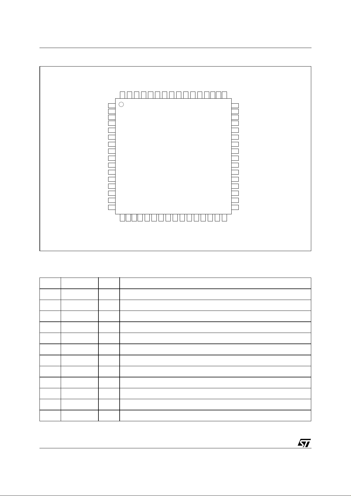
PIN CONNECTION
(Top view)
VCV1
VCV2
VCMP1
VCMP2
VCMGND1
VCMGND2
CPOSC
VCC5
DIG_GND
N_DRV
N_FEED
N_COMP
25_BASE
25_FEED
33_BASE
33_FEED
CT
OUTU1
RSEN4
VBOOST
64
01
02
03
04
05
06
07
08
09
10
11
12
13
14
15
16
OUTU2
CPOSCH
61
62
63
20212223242526272829303132
191718
RSEN3
60
59
58
VCV3
OUTV1
OUTV2
55
56
57
VCV4
VM1
VM2
53
54
Rsense
OUTW2
OUTW1
514950
52
RSEN2
48
RSEN1
47
VCMN2
46
VCMN1
45
VCMGND4
44
VCMGND3
43
SNS_N
42
SNS_P
41
SNS_OUT
40
ERR_OUT
39
ERR_IN
38
DAC_OUT
37
SCLK
36
SYSClk
35
SDATA
34
33
SEN
ZC
Skin
SkFin
CPOR
CBRAKE
VREF25
AGND
NPOR
Skout
SkFout
Timer1
SkDout
CalCoarse
PIN DESCRIPTI ON
N° Pin V Description
1 VCV1 S12 12V power supply
2 VCV2 S12 12V power supply and POR sensing threshold
3 VCMP1 O12 VCM positive output
4 VCMP2 O12 VCM positive output
5 VCMGND1 gnd VCM power ground
6 VCMGND2 gnd VCM power ground
7 CPOSC O12 Charge pump oscillator
8 VCC5 S5 5V power supply
9 DIG_GND gnd Digital & Switching regulator ground
10 N_DRV O5 Neg Reg ext FET gate driver
11 N_FEED I5 Neg Reg feedback
Test
ADaux
VCMBEMF
12 N_COMP IO5 Neg Reg error output
2/46
Page 3

L7250
PIN DESCRIPTI ON
N° Pin V Description
13 25_BASE O5 Reg 1.8V ext NPN base
14 25_FEED I5 Reg 1.8V feedback
15 33_BASE O5 Reg 3.3V ext NPN base
16 33_FEED IO5 Reg 3.3 V feedback
17 CPOR IO5 POR delay capacitor
18 NPOR O5 POR output signal
19 CBRAKE IO5 Spindle brake capacitor
20 AGND gnd analog gnd
21 VREF25 IO5 2.5V reference
22 ZC O5 Spindle zero crossing
23 Skin I5 Shock sensor input
24 Skout O5 Shock sensor 1st opamp output
25 SkFin I5 Shock sensor filter input
26 SkFout O5 Shock sensor filter output
(continued)
27 SkDout O5 Shock sensor output
28 Timer1 IO5 Timer 1 for unload procedure
29 CalCoarse I5 VCM BEMF coarse calibration
30 ADaux I5 auxiliary input for the ADC
31 VCMBEMF O5 VCM BEMF processor output
32 Test IO5 used for testing porpouse (*)
33 SEN I5 Serial enable
34 SDATA IO5 Serial data
35 SYSClk I5 System clock
36 SCLK I5 Serial clock
37 DAC_OUT O5 VCM DAC output
38 ERR_IN I5 VCM error opamp input
39 ERR_OUT O5 VCM error opamp output
40 SNS_OUT O5 VCM sense opamp output
41 SNS_P I12 VCM sense opamp positive input
42 SNS_N I12 VCM sense opamp negative input
43 VCMGND3 gnd VCM power ground
3/46
Page 4

L7250
PIN DESCRIPTI ON
N° Pin V Description
44 VCMGND4 gnd VCM power ground
45 VCMN1 O12 VCM negative output
46 VCMN2 O12 VCM negative output
47 RSEN1 O12 Spindle power sensing resitor
48 RSEN2 O12 Spindle power sensing resitor
49 Rsense I5 Spindle sensing resistor input
50 OUTW1 O12 Spindle phase C output
51 OUTW2 O12 Spindle phase C output
52 VM1 IO12 Vmotor
53 VM2 IO12 Vmotor
54 VCV4 S12 12V power supply
55 VCV3 S12 12V power supply
56 OUTV1 O12 Spindle phase B output
57 OUTV2 O12 Spindle phase B output
(continued)
58 RSEN3 O12 Spindle power sensing resitor
59 RSEN4 O12 Spindle power sensing resitor
60 OUTU1 O12 Spindle phase A output
61 OUTU2 O12 Spindle phase A output
62 CT I12 Spindle central tap
63 CPOSCH IO20 Charge pump diodes connection
64 VBOOST IO20 Charge Pump voltage
(*) used al so to set the IC power supply applicati on. If this pin is pull-up exter nal l y the L7250 be came a 5V appl i cation
S = Supply ; IO = Input/Output ; I = Input ; O = Output ; gnd = Ground.
4/46
Page 5

ELECTRICAL CHARACTERISTCS
ABSOLUTE MAXIMUM RATINGS
Symbol Parameter Value Unit
VCV1,VCV2,VCV3,VCV4 14 V
VCC5 maximum voltage 6 V
L7250
OUTU1,OUTU2,OUTV1,OUTV2,OUTW1,OUTW2
VCMP1,VCMP2,VCMN1,VCMN2
VM1,VM2
Digital Input Voltage -0.3 to VCC5 V
Operating free-air temperature 0 to 70 °C
Storage Temperature -55 to 150 °C
-1V to 16 V
ELECTRICAL CHARACTERISTCS
POWER SUPPLY [VCC5 & VCV] VCC5 = 5V ±10%, VCV = 12V ±10%. T
Symbol Parameter Test Condition Min. Typ. Max. Unit
POWER MONITOR, SUPPLY CURRENTS, ETC.
Icc5 VCC5 Operating current Spindle and VCM enabled, no
load
Ivcv VCV + VRET Operating current Spindle and VCM enabled, no
load
CHARGE PUMP VOLTAGE BOOSTER
VBOOSTCharge pump output voltage VCV = 12V
Iload = 5mA
= 25°C (unless otherwise specified)
amb
9mA
44 mA
18.5 V
VBOOS
Tfreq
POWER MONITOR
vt5 VCC5 threshold 4.0 4.175 4.35 V
vt12 VCC12 threshold 9 9.5 10 V
hv5 VCC5 hysteresis 40 100 160 mV
hv12 VCC12 hysteresis 100 200 300 mV
vt33 V33 Threshold 2.7 2.8 2.9 V
hv33 V33 Hysteresis 20 40 60 mV
vt18 V18 Threshold (at pin 25_FEED) 1.07 1.12 1.17 V
hv18 V18Hysteresis 25 50 75 mV
NPOR
Switching frequency 1 MHz
NPOR low level output voltage VCV > 4.5V Iol = 5mA 0.75 V
low
5/46
Page 6
L7250
ELECTRICAL CHARACTERISTCS
POWER SUPPLY [VCC5 & VCV] VCC5 = 5V ±10%, VCV = 12V ±10%. T
(continued)
= 25°C (unless otherwise specified)
amb
Symbol Parameter Test Condition Min. Typ. Max. Unit
NPOR
NPOR internal pull_up resistor to
pull
6Kohm
V33
CPOR
CPOR
CPOR charging current Vout = 0V 5 uA
Ic
CPOR low level output voltage VCV > 4.5V Iol = 1mA 50 mV
low
Vref25 2.5V reference voltage -5% 2.5 +5% V
THERMAL WARNING AND THERMAL SHUTDOWN
T
warn
Thermal warming temperature Characterized, tested by
130 140 150 °C
correlation.
Tsoff Thermal Shutdown temperature Characterized, tested by
150 165 180 °C
correlation
Thys Thermal Hysteresis valid for both temperature
20 25 30 °C
thresholds
VM ISOLATION FET
IsoR Rds ON @ 125°C , I=2.5A 0.1 Ohm
IsoI Continuous current 2.5 A
SPINDLE DRIVER SECTION
POWER STAGE
Rds(on) Total output ON resistance
@ 125°C, I=2.5A 0.9 Ω
(Source + Sink)
Idsx Output leakage current -200 -500 µA
CTlkg Centarl tap leakage 1 µA
DiodeFw Clamp diode forward voltage If = 2.5A 0.6 1.2 V
Slew Output slew rate OUTx 10% to 90%
40 V/µS
Reg04H ‘b7b6b5’ = 011
BACK EMF COMPARATOR
Vie Common mode input voltage
Guaranteed by design 0 VM V
range.
Vr Input voltage range where output
Guaranteed by design -1 VM+1 V
shall not invert.
BEMFoff BEMF input offset CT = 6V -15 +15 mV
BEMFhy BEMF hysteresys CT = 6V 50 mV
SPINDLE CURRENT LIMITING
Iin RSENSE Input bias current. 0 < Vin < 3.3V 1 µA
CURoff Comparator offset -15 +15 mV
6/46
Page 7
L7250
ELECTRICAL CHARACTERISTCS
POWER SUPPLY [VCC5 & VCV] VCC5 = 5V ±10%, VCV = 12V ±10%. T
(continued)
= 25°C (unless otherwise specified)
amb
Symbol Parameter Test Condition Min. Typ. Max. Unit
CURdacr
CUR
CUR
CUR
DAC resolution 3 bit
DAC output Reg04H ‘b4b3b2’ = 000 250 mV
dac_L
DAC output Reg04H ‘b4b3b2’ = 111 600 mV
dac_H
DAC linearity -10 +10 mV
lin
Cbrake
Icbrake VCbrake leakage VCbrake=5V 1 µA
VCM SECTION
CURRENT SENSE AMPLIFIER
Vts Common mode input voltage
GBD - not tested -0.6 VM+1 V
range.
Sns _vof
Sns_gai n0
f Input offset voltage -12 12 mV
Differential Voltage GAIN0 Reg09H ‘b7’ = 0 -5% 4.5 +5%
Sns _gain1
Sns_low
Sns_high
sns_slew
Sns_band
sns _cmrr
sns _svrr
Differential Voltage GAIN1 Reg09H ‘b7’ = 1 -5% 16 +5%
VSENSE output saturation
voltage
Iload=+/-1mA
Vin_diff=+/- 500m V
4.75
250 mV
V
Output slew rate Cload=50pF 1 V/µs
-3dB Bandwidth Guaranteed by design 200 400 kHz
Common mode rejection ratio f < 10 KHz, tested at DC only
CMRR=A
V DIFF/AV CM
70 dB
supply voltage rejection ratio VCV f < 10 KHz, tested at DC only 60 dB
ERROR SUMMING AMPLIFIER
err _gain Voltage gain no load 60 dB
err _band
Unity gain bandwidth Guaranteed by design 4 MHz
err _slew Output Slew Rate Cload=50pF 1.5 V/µS
err _ibias
Input bias current 1 µA
err _off Input offset voltage -10 0 10 mV
err_svrr supply voltage rejection ratio f < 10 KHz, tested at DC only 60 dB
err _clamp
Low output (clamp) voltage Isink = 1 mA, referred to Vref25 TBD V
low
7/46
Page 8
L7250
ELECTRICAL CHARACTERISTCS
POWER SUPPLY [VCC5 & VCV] VCC5 = 5V ±10%, VCV = 12V ±10%. T
Symbol Parameter Test Condition Min. Typ. Max. Unit
err _clamp
high
VCM OUTPUT DRIVERS
PWR_Gain
Rds(on) Total output ON resistance
PWR_Lkg
DiodeFw Clamp diode forward voltage If = 2A 0.6 1.2 V
THD Total Harmonic Distortion characterized no tested 1 %
PWR_Slew
PWR_B
and
Icross Static Shoot-through current Guaranteed by design 0 mA
VCM CURRENT CONTROL LOOP STATIC AND DYNAMIC CHARACTERISTICS
IVCMoff Total offset current Rs=0.2 -75 75 mA
High output (clamp) voltage Isource = 1mA, referred to Vref25 TBD V
Power amplifier differential gain. Io = ±1A, Rload = 8Ω 14 15 16 V/V
(Source + Sink)
Output leakage current 600 uA
VCMN or VCMP slew rate RL = 8 ohms 1 V/us
Power Amp -3dB Bandwidth Driving ERROUT = VDACREF,
(continued)
@ 125°C, I=2A .9 Ω
Guaranteed by design
= 25°C (unless otherwise specified)
amb
250 500 kHz
DIVCMoff
Gm_psrr Gm loop VSRR of VCV -1 1 mA/V
VCM LINEAR DAC
DAC_res Resolution 15 bit
DAC_out Full Scale Output Voltage wrt VDACREF 0.96 1 1.04 V
DAC_off Mid-Scale Error wrt VDACREF -12 12 mV
DAC_DNL
DAC_INL
DAC_Co
nvT
VCM LOAD/UNLOAD
ADC
ADC_res
ADC_DNL
ADC_INL
Total offset current drift
temperature coefficient
Differential Non linearity Guaranteed Monotonicity ±1 LSB
Integral Non Linearity ±64 LSB
Conversion time 90% from 3FFFh to 0020h 3 µs
resolution 10 bit
Differential Non Linearity 1 LSB
Integral Non Linearity 3 LSB
Guaranteed by design .2
mA/oC
ADC_Co
nvT
8/46
Conversion time 40 ADC
Clock
cycles
Page 9
L7250
ELECTRICAL CHARACTERISTCS
POWER SUPPLY [VCC5 & VCV] VCC5 = 5V ±10%, VCV = 12V ±10%. T
Symbol Parameter Test Condition Min. Typ. Max. Unit
ADC AUXILIARY INPUT
AUX_ran
ge0
AUX_ran
ge1
AUX_Ibias
VCM VOLTAGE AMPLIFIER
V olt_gain
Volt_off Input offset -15 +15 mV
Vo lt
_cmrr
Volt
_svrr
BEMF processor amplifier
CalCoar
seIn
Input range 0 Reg06H ‘b3’ = 0
Input range 1 Reg06H ‘b3’ = 1
Input bias -100 100 µA
Voltage gain 0.165 V/V
Common mode rejection ratio f < 10 KHz, tested at DC only
supply voltage rejection ratio f < 10 KHz, tested at DC only 60 dB
Calcoarse voltage input range 0.5 2 V
(continued)
Referred to Vref25
Referred to Vref25
CMRR=A
V DIFF/AV CM
= 25°C (unless otherwise specified)
amb
±1 V
±2.25 V
46 dB
Gain1 First stage gain Vcontrol = 1.25 V 1.91 V/V
Gain2 Second stage gain 16 V/V
Offset Residual input offset after
calibration
Rout BEMF amp output resistance (pin
31)
ULOAD @ POR
Timer1_V
Timer1_I Timer1 Discharging Current 2 µA
Timer1_T
VOLTAGE REGULATORS
1.8 AND 3.3 LINEAR REGULATOR
V18 feed 1.8V feedback Voltage -5% 1.25 +5% V
V33 OUT
Timer1 Charging Voltage 2.5 V
Timer1 Low threshold 0.2 V
3.3V Output Voltage -5% 3.3 +5% V
Vcontrol = 1.25V
(Measured between VCMN and
SNS_P pins)
-3 +3 mV
500 ohm
9/46
Page 10

L7250
ELECTRICAL CHARACTERISTCS
POWER SUPPLY [VCC5 & VCV] VCC5 = 5V ±10%, VCV = 12V ±10%. T
Symbol Parameter Test Condition Min. Typ. Max. Unit
V18
IDRIVE
V33
IDRIVE
NEGATIVE REGULATOR
FREQ0 Oscillator frequency Default configuration 500 KHz
FREQ1 Oscillator frequency TestRegister = ‘00001001’
VoutH High level output voltage TBD V
VoutL Low level output voltage TBD V
VNEerr
OFFS
VNEGerr
BIAS
Vneg_err
_cmrr
Vneg_err
_svrr
Output base current drive
Feedback input offset -10 10 mV
Feedback input bias 0 1 µA
Common mode rejection ratio f < 10 KHz, tested at DC only
supply voltage rejection ratio VCV f < 10 KHz, tested at DC only 60 dB
(continued)
or = ‘00101001’
CMRR=A
V DIFF/AV CM
= 25°C (unless otherwise specified)
amb
1 MHz
46 dB
15 mA
SHOCK SENSOR
SkIgain0 Input OPAMP gain0 Reg02H ‘b7’ = 0 10 V/V
SkIgain1 Input OPAMP gain1 Reg02H ‘b7’ = 1 80 dB
SkIoff Input OPAMP offset -15 +15 mV
SkIinput Input OPAMP input impedance Reg02H ‘b7’ = 0 10 Mohm
SkFgain Filter OPAMP open loop gain 80 DB
SkFband Filter OPAMP unity gain
bandwidth
SkFoff Filter OPAMP offset voltage -10 +10 MV
SkOThH0
SkOThH1
SkOThL0
SkOThL1
Output window comparator
VthHigh
Output window comparator
VthHigh
Output window comparator
VthLow
Output window comparator
VthLow
Guaranteed by design 5 Mhz
Referred to Vref25 ;
Reg02H ‘b6’ = 0
Referred to Vref25 ;
Reg02H ‘b6’ = 1
Referred to Vref25;
Reg02H ‘b6’ = 0
Referred to Vref25;
Reg02H ‘b6’ = 1
200 mV
500 mV
200 mV
500 mV
10/46
Page 11

L7250
ELECTRICAL CHARACTERISTCS
POWER SUPPLY [VCC5 & VCV] VCC5 = 5V ±10%, VCV = 12V ±10%. T
Symbol Parameter Test Condition Min. Typ. Max. Unit
SERIAL PORT
Voh Logic Output voltage high Ioh=1mA 2.7 V
Vol Logic Output voltage low Iol=1mA 0.5 V
Vih L ogic input high Iih=1uA 2.2 V
Vil Logic input low Iil=-1uA 0.5 V
Iih Logic high input current Internal Pulldown Resistor
Iil Logic low input current -1.00 µA
(continued)
Vin = 3.3V
= 25°C (unless otherwise specified)
amb
33 µA
1 SERIAL PORT
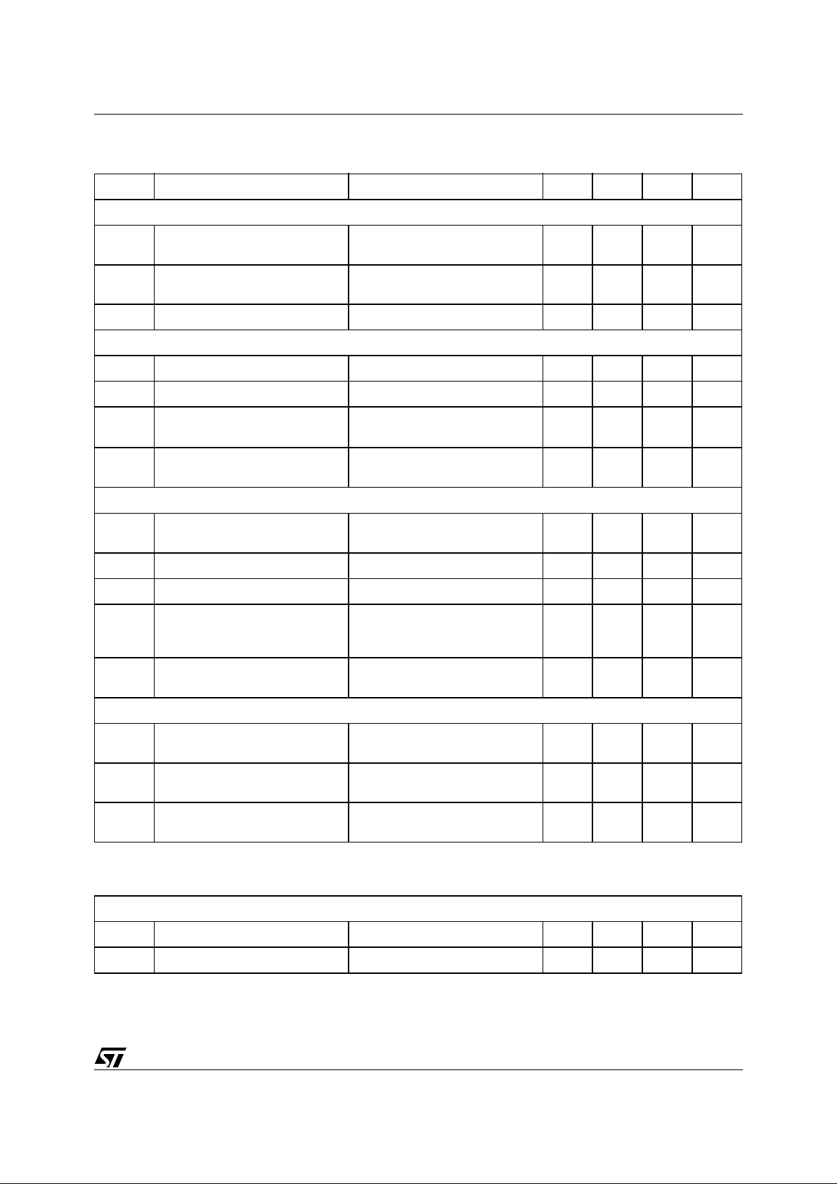
The serial port is a bidirectional three pi n interface, using SDATA, SCLK and SE N to addr ess and communi cate
with sixteen 8 bit registers in the L7250. These registers include the status register, Spindle control registers,
VCM control registers, sinewave drive registers, and test mode register. These registers are cleared to zero at
power up.
1.1 Default comunication modes setting (bit 7, Reg05H ) = 0
After the SEN falling edge, the internal state machine is waiting for the first SCLK falling edge. This means that
if the SCLK line starts from an high level the first falling edge, respecting the setup time Tefcf, is considered,
and is used to read the R/W bit. During a writing process the internal state machine must see 16 SCLK falling
edges to validate the operation. The write mode is started if the R/W bit is low on the first falling edge of SCLK.
The read mode is started if the R/W bit is high on the first falling edge of SCLK. The ID, Address, and Data are
all then subsequently read by the L7250 on the falling edges of SCLK. (See Figure 1)
The microcontroller has to read the data on the falling edge of the SCLK signal. After the hold time (Tedh) the
data line switches to the next data without a tri-state phase.During a read mode the last address bit is read by
L7250 on the eighth falling edge of SCLK. The internal state machine then turns the SDATA bit around for the
L7250 to assume control at the next SCLK rising edge (the first rising edge after the 8th SCLK falling edge).
11/46
Page 12
L7250
Figure 1. Default serial port timing diagram (bit 7, Reg05H = 0)
Teh
Tcfer
Tcrer
D1 D0
D2
D0
Tedh
D5 D4 D3
D6
D6 D5 D4 D3 D2 D1
D7
Tdly
Tcdd
L 7250 takes bus control
Tcds Tcdh
A1 A0 D7
A2
A1 A0
A2
Tcc Tch Tcl
ID2 ID2 A2
ID2 ID2 A2
ID 2
Tefcf
SEN
Note1: During writing process L7250 latches the data on the SC LK falling edge (the ASI C is writing on the SCLK
rising edge)
Note2: During reading process L7250 takes the bus control on the next SCLK rising edge after the 8th SCLK
falling edge
The L7250 write the data on the SCLK falling edge respecting the data hold time (Tedh)
Note3: The ID number for the L7250 is ID1=ID2=ID3=1
12/46
SCLK
W
SDATA
(w rite)
ID 2
R
SDATA
(read)
Page 13

1.2 Default serial port timing Table
Symbol Parameter Min Max Unit
Tcc Serial clock period 30 ns
Tch Serial clock high time 13 ns
Tcl Serial clock low time 13 ns
Tcds Serial data setup time to clock falling edge (write mode) 5 ns
Tcdh Serial clock falling edge to serial data hold time (write mode) 4 ns
Tedh Serial clock falling edge to serial data hold time (read mode) 5 ns
Tcdd Serial data setup time to clock falling edge (read mode) 5 ns
Tel Serial Enable low time 490 ns
Teh Serial Enable high time 30 ns
Tefcf Serial Enable falling edge to serial clock falling edge 17 ns
Tcfer Serial clock falling edge to Serial enable rising edge 17 ns
Tdly SDATA turn around delay time 0 ns
L7250
Note 1: All specifications with respect to 50% of signal switching thresholds
Note 2: Reading mode tested at M ax 20Mhz
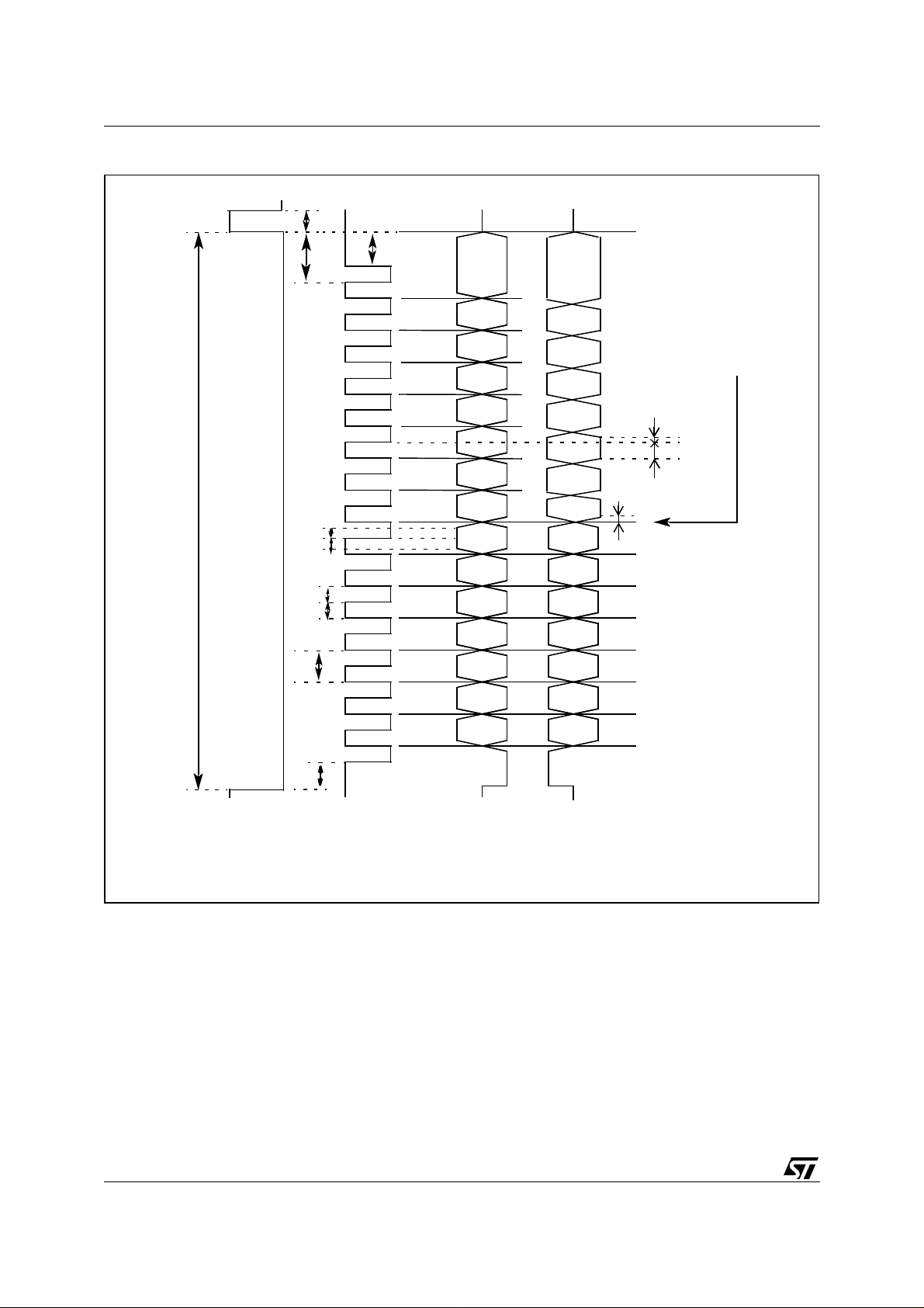
1.3 Inverted clock comunication modes (bit 7, Reg05H) = 1
To set the bit7, Reg05H to 1, entering this different comunication mode, a writing process using the default comunication protocol (see the above paragraph) must be used.
After the SEN falling edge, the internal state machine is waiting for the first SCLK rising edge. This means that
if the SCLK line starts from a low level the first rising edge, respecting the setup time Tefcr, is considered, and
is used to read the R/W bit. The internal state machine must see 16 SCLK rising edges to validate the write
operation. The write mode is started if the R/W bit is low on the first rising edge of SCLK. The read mode is
started if the R/W bit is h igh on the first rising ed ge of SCLK. The ID, Address, and Data are a ll then subsequently read by the L7250 on the rising edges of SCLK (See Figure 2).
The microcontroller has to r ead (l atch) the data on the falli ng edge of the SCLK signal. L7250 pr esents the data
on the SCLK rising edge. During a read mode the last address bit is latched by the L7250 on the eighth rising
edge of SCLK. The internal state machine then turns the SDATA bit around for the L7250 to ass ume control at
the next SCLK falling edge (the first falling edge after the 8th SCLK rising edge).
13/46
Page 14
L7250
Figure 2. Inverted clock serial port timing diagram (bit 7, Reg05H = 1)
Teh
Tcrer
D1 D0
D2
D0
Tedh
D5 D4 D3
D6
Tel
D6 D5 D4 D3 D2 D1
D7
Tdly
Tvld
L7250 takes bus control
Tcdh
Tcds
A1 A0 D 7
A1 A0
Tcl
A2
A2
Tch
Tcc
ID 2 ID2 A2
ID 2 ID2 A2
ID 2
Tefcr
SEN
Note1: During writi ng proc ess L7250 l atches the data on the SCLK ris ing ed ge ( the ASIC is w riting on the S CLK
falling edge)
Note2: During reading proces s L7250 takes the bus c ontrol on the next SCLK falling edge after the 8th SCLKrising edge
The L7250 write the data on the SCLK rising edge and it is expec ting the ASIC to latches the data on the SCLK
falling edge
Note3: The ID number for the L7250 is ID1=ID2=ID3=1
14/46
SCLK
W
SDATA
(w rite)
R
SDATA
ID 2
(read)
Page 15

1.4 Inverted clock serial port timing Table
Symbol Parameter Min Max Unit
Tcc Serial clock period 30 ns
Tch Serial clock high time 13 ns
Tcl Serial clock low time 13 ns
Tcds Serial data setup time to clock falling edge (write mode) 5 ns
Tcdh Serial clock falling edge to serial data hold time (write mode) 4 ns
Tedh Serial clock falling edge to serial data hold time (read mode) 5 ns
Tvld Serial clock rising edge to SDATA stable time (read mode)
Cload=5pF (see Note2)
Cload=50pF (see Note2) 11
15
Tel Serial Enable low time 490 ns
Teh Serial Enable high time 30 ns
Tefcr Serial Enable falling edge to serial clock rising edge 17 ns
Tcrer Serial clock rising edge to Serial enable rising edge 17 ns
L7250
ns
ns
Tdly SDATA turn around delay time 0 ns
Note 1: All specifications with respect to 50% of signal switching thresholds
Note 2: In reading mode the clock frequency is li m i ted by this pa ram eter;
in fact the min ‘serial clock high time’ is defined by (Tvld+Tasu)
where Tasu = min ASIC setup time
15/46
Page 16

L7250
Table 1. Register Map
addr b7 b6 b5 b4 b3 b2 b1 b0 name
00H SPNCurrSignVCMcalOut ZCBad
ThShutdown
ThWarn rev2 rev1 rev0 SR status readonly
mnemoni
c
attributes
01H RLvoltage1
02H ShockConf ShockTh[0]
03H BemfOffCal VCMState2 VCMState1 VCMSt ate0 SP state3 SPstate2 SPstate1 SPstate0 CTR1 SP&VCMst
04H SPslew2 SPslew1 SPslew0 Cu rdac2 Curdac1 Curdac0
05H SPIprot m3 m2 m1 m0 TSDen VnegEn Sken CTR3 control read/write
06Hw4w3w2w1w0
07H LoadCP Adv a nc e FFWEn TO4 TO3 TO2 TO1 TO0 CTR5 control read/write
08H Kv7 Kv6 Kv5 Kv4 Kv3 Kv2 Kv1 Kv0 KVR Kv a l read/write
09H GainSwitch dac14 dac13 dac12 dac1 1 dac10 dac9 dac8 DAR1 DAC reg 1 read/write
0AH dac7 dac6 dac5 dac4 dac3 dac2 dac1 dac0 DAR2 DAC reg 2 read/write
0BH ADC_DATA
0CH ADC_DAT A
0DH reserved reserved reserved reserved reserved reserved reserved reserved read/write
0EH reserved reserved reserved reserved reserved reserved reserved reserved read/write
0FH test7 test6 test5 test4 test3 test2 test1 test0 TEST test read/write
RLvo ltage1
[1]
ADC_DATA
(9)
ADC_DATA
(1)
RLvo ltage2
[0]
RL ToffBrake
ADC_DATA
(8)
ADC_RES
(0)
_ADDR(1)
RLvoltage2
[1]
RL ToffBrake
[1]
ADC_DATA
(7)
ADC_RES
_ADDR(0)
Rltimer[2] Rltimer[1] Rltimer[0] NoBrake VCM1 VCM RLreg read/write
[0]
Rlcalib[3] Rlcal ib[2] Rlcalib[ 1] Rlcalib[0] VCM2 VCMR L reg read/write
[0]
ADC_DATA
(6)
ADCRange ADC_CH_
PREADC(1) PREADC(0)
ADC_DATA
(5)
ADDR(1)
PWMmask 1 PWMmask0
ADC_DATA
(4)
ADC_CH_
ADDR(0)
PREsm o CTR4 control read/write
ADC_DATA
(3)
(2)
ADC_START
CTR2 control read/write
ADR ADC reg readonly
ADR ADC reg read/write
read/write
ate
16/46
Page 17

L7250
Table 2. Register map content description
Bit SPI field name Content
REGISTER SR, ADDRESS: 00H
[2:0] Rev[2:0] Revision number of the device, set internally
[3] ThWarn Thermal warning
[4] ThShutdown Thermal shutdown
[5] ZCbad Signals a problem with spindle speed loop synchronism
[6] VCMcalOut VCM error output in calibration mode
[7] SPNCurrSign Spindle current sign to implement adaptive torque optimizer
REGISTER VCM1, ADDRESS: 01H
[0] NoBrake 0=VCM active brake phase enabled
[3:1] Rltimer[2:0] 000 = only Unload1 is enabled
(continued)
control
1= VCM active brake phase disabled
001 = threshold set to 0.4V
010 = threshold set to 0.8V
011 = threshold set to 1.2V
100 = threshold set to 1.6V
101 = threshold set to 2V
110 = threshold set to 2.4V
111 = only Unload2 is enabled
[5:4] Rlvoltage2[1:0] Selects between 4 values of unload voltage in Unload2 phase:
00 = 1V
01 = 1.125V
10 = 1.250V
11 = 1.375V
[7:6] Rlvoltage1[1:0] Selects between 4 values of unload voltage in Unload1 phase:
REGISTER VCM2, ADDRESS: 02H
[3:0] Rlcalib[3:0] 0111 = 29.4%
00 = 0.375V
01 = 0.5V
10 = 0.625V
11 = 0.75V
0110 = 25.2%
0101 = 21%
0100 = 16.8%
0011 = 12.6%
0010 = 8.4%
0001 = 4.2%
0000 = 0%
1111 = -4.2%
1110 = -8.4%
1101 = -12.6%
1100 = -16.8%
1011 = -21%
1010 = -25.2%
1001 = -29.4%
1000 = -33.6%
17/46
Page 18

L7250
Table 2. Register map content description
Bit SPI field name Content
[5:4] RLToffBrake[1:0] Selects the duration of Toff (Ton) active brake phase:
[7] SkockConf Selects the Shock Sensor application
[6] SkockTh[0] Selects the Shock Sensor threshold
REGISTER CTR1, ADDRESS: 03H
[3:0] Spstate[3:0] 0000 = CLCOAST
[6:4] VCMstate[2:0] Possible states for the VCM:
(continued)
00 = 300usec
01 = 400usec
10 = 500usec
11 = 600usec
0 = piezo element
1 = charging element
0 = Vref +/- 200mV
1 = Vref +/- 500mV
0001 = OLCOAST
0010 = OLSIX
0011 = OLSIN
0100 = OLBRAKE
0101 = INDSENSE
0110 = CLSIX
0111 = CLSIN
1000 = CLBRAKE
000 = Unload/Retract
001 = tri-state
010 = brake
011 = enable current mode
100 = enable voltage mode
101 = offset calibration
110 = confirm the previous state
111 = confirm the previous state
[7] BemfOffCal VCM BEMF processor offset calibration
REGISTER CTR2, ADDRESS: 04H
[1:0] PWMmask[1:0] Selects the length of the mask over PWM rising edge:
[4:2] Currdac[2:0] Selects the voltage threshold for the spindle current limiter:
18/46
00 = 2 us
01 = 4 us
10 = 6 us
11 = 8 us
000 = 250mV
001 = 300mV
010 = 350mV
011 = 400mV
100 = 450mV
101 = 500mV
110 = 550mV
111 = 600mV
Page 19

L7250
Table 2. Register map content description
Bit SPI field name Content
[7:5] Spslew[2:0] 000 = 10 V/us
REGISTER CTR3, ADDRESS: 05H
[0] Sken 0 = shock sensor output no latched
[1] Vnegen 0 = negative regulator disabled
[2] TSDen 0 = thermal shutdown disabled
[6:3] M[3:0] masking while sensing ZC, expressed in terms of half samples
[7] SPIprot 0 = default protocol
(continued)
001 = 20 V/us
010 = 30 V/us
011 = 40 V/us
100 = 50 V/us
101 = 60 V/us
110 = 70 V/us
111 = 80 V/us
1 = shock sensor output latched (to clear the latched information
a transition 1 -> 0 -> 1 is necessary)
1 = negative regulator enabled
1 = thermal shutdown enabled
after window opening
In terms of electrical degrees the single mask step is 3.75.
1 = inverted SCLK protocol
REGISTER CTR4, ADDRESS: 06H
[0] PREsmo 0 = spindle clock is system clock divided by two (FFWDADC clock
is system clock divided by 8)
1 = spindle clock is system clock (FFWDADC clock is system
clock divided by 4)
[2:1] PREADC[1:0] 00 = sleep mode
01 = ADC clock is system clock divide by 4
10 = ADC clock is system clock divide by 2
11 = ADC clock is system clock
[7:3] W[4:0] Windowing while sensing ZC, expressed in terms of half samples
before TO value
In terms of electrical degrees the single window step is 3.75.
REGISTER CTR5, ADDRESS: 07H
[4:0] TO[4:0] Coarse and fine section of phase shift, applied for torque
[5] FFWEn 0 = power supply compensation for spindle disabled
[6] Advance 0->1 increments by one the current sample position
[7] LoadCP 0->1 enables load of TO value as the current sample position
REGISTER KVR, ADDRESS: 08H
optimization.
In terms of electrical degrees the Torque Optimizer single step is
0.937 electrical degrees.
1 = power supply compensation for spindle enabled
[7:0] Kv[7:0] KVAL factor for speed loop control
19/46
Page 20

L7250
Table 2. Register map content description
Bit SPI field name Content
REGISTER DAR1, ADDRESS: 09H
[6:0] Dac[14:8] 7 MSB for VCM dac
[7] GainSwitch 0 = gain voltage of the VCM sense amplifier equal to 4.5 V/V
REGISTER DAR2, ADDRESS: 0AH
[7:0] Dac[7:0] 8 LSB for VCM dac
REGISTER ADR, ADDRESS: 0BH
[7:0] ADC_DATA[9:2] 8 MSB output data from ADC conversion
REGISTER ADR, ADDRESS: 0CH
[0] ADCSTART 0-> 1 starts a new ADC conversion
[2:1] ADC_CH_ADDR[1:0] Channel whose conversion is required
[3] ADCrange 0 = the 4 signals enter directly (maintaining the proper dynamic
(continued)
1 = gain voltage of the VCM sense amplifier equal to 16 V/V
00 = VCM current sense amplifier output
01 = VCM voltage amplifier output
10 = VCM BEMF
11 = Auxiliary Channel (external pin)
range) the ADC block
1 = the 4 signals are scaled down to the ADC dynamic range
[5:4] ADC_RES_ADDR[1:0] Channel whose result conversion is currently present in
REGISTER ADR, ADDRESS: 0DH
0DH [7:0] reserved
REGISTER ADR, ADDRESS: 0EH
0EH [7:0] reserved
REGISTER ADR, ADDRESS: 0FH
0FH [7:0] Test[7:0] Test register
ADC_DATA
20/46
Page 21

2 SPINDLE MOTOR CONTROLLER
(
)
Figure 3.
REGISTER
KVAL
MULTIPLIER
ZERO
CROSSING
PERIOD
COUNTER
16+4 BIT
KVAL
DIGI TAL
6 State
or
Sine
Mode
COARSE
PHASE
ADVANCE
BITS
LOADCP
BIT
OLSIX/O L SIN
OR CLSIX/CLSIN
ADVANCE
BIT
FINE
PHASE
ADVANCE
BITS
SMOOTHDRIVE
RAW
DUTY CYCLE
SMOOTHDRIVE
PROFILE
MEMORY/
LOGIC
MEMORY
ADDRESS
COUNTER
N=48
FSCAN
FSCAN
COUNTERZCTc
SYSCLK
16.5MHZ
SMOOTHDRIVE
MODULATED
DUTY CYCLE
START-OF-COUNT
WINDOW
TRISTATE
CMD
WINDOW
MASK
PWM MASK
MASK
REGISTERS
COMPENSATION
COUNTER
&
COM PA R ATOR S
CURRENT
COMP.
SUPPLY
VOLTAGE
ADC
BEMF
COMP.
LIMIT
VM
TIME DOMAIN
DUTY CYCLE
SIGNALS
FET
GATE
DRIV E
FET
GATE
DRIV E
FET
GATE
DRIV E
CUR DAC
L7250
VM
HGU
MOTU
LGU
VM
HGV
MOTV
LGV
VM
HGW
MOTW
LGW
CTAP
xx
SPSENH
xx
SPINDLE
MOTOR
2.1 Spindle Sm oothdrive Functionality
L7250 utilizes ST's proprietary Smoothdrive commutation algorithm. Smoothdrive is a voltage mode pseudosinusoidal spindle drive scheme where the duty cycles of the three windings are modulated to form sinusoidal
voltages across each winding. The system determines the shape and amplitude of the driving voltages in a
completely digital manner.
2.2 SYSCLK
The Smoothdrive system clock comes through the SYSCLK pin.
The system expects eit her 33MH z or 16.5M Hz on t his pi n, and needs 16.5MH z internally. A SYSCLK divide by
two can be enabled by a SPI register bit PRESMO to accomodate a 33MHz external clock.
2.3 Smoothdrive Wave shape
The basic Smooth drive wave shape is stored in digital memory. A voltage profile designed to reduce switching
losses and increase th e voltage headr oom has been im plemented. Essenti ally, two phas es are PWM' ed, while
the low side driver of the third phase is on at 100% duty cycle. The PWM duty cycles are modulated in such a
way as to result in sinusoidal cur rents on all 3 motor phases. Driv ing in this manne r, as opposed to dri ving true
sinusoids on all three phases, results in improved headroom and effici ency, appr oachi ng that of conventional 6
state commutation.
The system is phase locked to the motor by sensing one BEMF zero crossi ng on one winding, once per electrical
21/46
Page 22

L7250
cycle. A window is opened up in that winding, and it is tri-stated to allow sensing of the zero crossing. The width
of the window opening is programmable, and can be made very small in steady stat e. A frequency lock ed loop
keeps the wave shape in sync with the motor speed. The system is entirely digital, requiring no external components.
The Smoothdrive wave shape is sync with the motor. It divides the electrical period, from one zero crossing to
the next, into 48 evenly spaced sample periods. For each sample period, the driving duty cycle is defined for
each motor phase by a table in the Smoothdrive logic. The Memory Address Counter sequences the samples
through the cycle, and is clocked N times per cycle. The following describes how the frequency locked loop
system works:
There are N sine wave samples per electrical rev. N=48 for this design.
Each electrical period (from one ZC to the next) is measured by a timer with an effective frequency of Fsysclk/
48, resulting in a measured zero crossing period Tc. The timer does not actually run at Fsysclk/48 - the resolution is more like Fsysclk/3.
The FSCAN Counter is a down counter preloaded with Tc, and running at Fsysclk. The FSCAN Counter puts
out a pulse each time it hits zero, then it resets to Tc and counts down again. This cycle occurs N (48) times
per electrical cyc le. Thus, t he FSCAN Counter divides the el ectr ical cycl e into N ev enly spaced s amples based
on the previous Tc. The pulse signal out of this block, that occurs 48 times per electrical period, is called FSCAN.
The Memory Address Counter counts FSCAN pulses, and tells the Profile Logic which full scale duty cycle values to use for each Smoothdrive sample period.
2.4 PWM rate
The PWM rate is unrelated to the Smoothdrive sample rate. The minimum PWM rate is 32.2kHz with 16.5MHz
spindle system cl ock, defined by (Fsys /512). The spin sy stem clock is SYSCLK or SYSCLK/2, chosen via s erial
port (SYSCLK/2 is the default at power up). 9 bits of resolution define the duty cycle at each sample period.
The PWM counter is reset at the beginning of each electrical cycle (at the ZC).
The PWM duty cycle is defined for each of the two chopping phases by comparing the appropriate duty cycle
values to the counter. The duty cycle values are the result of multiplying values in the Smoothdrive waveform
table by the amplitude value KVAL coming from SPI.
2.5 Supply Voltage Compensation via ADC
The Smoothdrive system is a voltage mode drive scheme. Without compensation, the spindle drive amplitude
would be a proportion of the motor supply voltage. L7250 implements a supply voltage compensation scheme
whereby the drive amplitude is indipendent on motor supply voltage.
An internal 6 bit ADC reads the motor supply voltage variation (+/-10%), and the applied duty cycle is modified
to keep the applied voltage constant. A side effect is that the PWM frequency will be changed as well as the
duty cycle.
The ADC runs on a 4MHz clock derived from the SYSCLK (it is divided by 8 if the PRESMO bit is set to zero
else it is divided by 4). The conversion resul ts affects the PWM counter onc e per PWM cycle, nominally 32 kH z.
2.6 BEMF comparator Hysteresis
Since only one polarity ZC is detected, the BEMF comparator hysteresis no longer needs to contribute a time
offset. The hysteresis is zero on the significant edge, and is engaged on the other edge. Thus, larger values of
hysteresis can be used to provide noise immunity at low speed while coasting, without affecting ZC timing.
Hysteresis of 50mV provides adeguate sensitivity for detecting motion startup, while improving noise immunity
when the motor is moving very slow or is stationary.
2.7 Startup Algorithm Description
L7250's spindle motor startup is controlled by firmware, and consists of four distinct phases: Inductive Position
22/46
Page 23

L7250
Sense, to determine rotor position, Open Loop Commutation, which accelerates the motor to build up BEMF,
Synchronization , to measure motor speed and position, initializing the Smoothdrive system, and Closed Loop
Smoothdrive Commutation, the normal synchronous commutation mode to accelerate and run at speed.
2.7.1 Inductive Position Sense
Inductive position sen sing is achieved throug h a firmware routine that measur es the current rise time in each of
the six possible states (six steps profile), and uses this information to determine the rotor position.
The six steps profile still comes from the Profile Memory that contains 48 samples, but in this case there are
only six different configuration, each of them r epeated eight times; the line ar scansion of the memor y one sample at a time gives a new six step configuration every eight increments.
Before any operation can be done, the firmware routi ne must set the KVAL v alue present in S PI to the maximum
value (*1) , to saturate the PWM signals given to the motor, and put the Memory Address Counter in a known
position (*3); this is done keeping the motor in OLCOAST (*2) state and asserting a LoadCP command (*4) to
load the content of the torque optimizer related SPI register into the Memory Address Counter.
At this point, the present six steps configuration can be energized through the INDSENSE state (*5) , w aiting
for the current to reach the thre shold programmable vi a SPI (*6); the current lim iting comparator will be trigger ed
by this condition, and it's output will be visible at ZC pad. The current rise time will be measured and stored from
the ASIC (*7) .
The device automatically limits the PWM si gnals for the three phases to limit the cur rent, but the cur rents in the
windings must be recirculated from firmware putting the motor in OLCOAST (*8) state.
A burst of eight ADVANCE signals (*9) must be asserted from SPI to reach the next configuration in the profile
memory, then the procedure can be r epeated. Each w inding can be e xcited mor e than one ti me, to av erage the
measurements, and at the end of the sensing sequence the ASIC decides the rotor position.
Figure 4. Inductive Sense Routine
START
Inductive Sense Routine
Nadv=0 , Nph=0
(*2)
(*1)
(*3)
(*4)
(*5)
(*6)
ZC=0
Set OLCOAST
Write Reg.03 H
Spstate[3:0] = 0001
Set KVAL
Write Reg.08 H
Kv[7:0] = 11111111
Set Torque Optimizer
Write Reg.07 H
TO[4:0] = 00000
Set Load Coarse Phase
Write Reg.07 H
LoadCP = 1
Set INDUCTIVE SENSE
Write Reg.03 H
Spstate[3:0] = 0101
Measure Current
Rise Time
By reading the
ZC
(pin 22)
ZC=1
Nph = 48
Nadv=0
YESNO
YES
Nadv=8
Inc Nadv
Inc Nph
Set ADVANCE
Write Reg.07 H
Advance = 1
Wait for
Current Decay
Set OLCOAST
Write Reg.03 H
Spstate[3:0] = 0001
Store the measured
Current Rise Time
& Nph associated
NO
(*9)
(*8)
(*7)
Compare the Six
Measured Rise Time
to define the
ROTOR POSITION
EXIT
Inductive Sense
Routine
23/46
Page 24

L7250
2.7.2 Open Loop Commutation
After position sense is complete, the microcontroller commutates the motor following a constant acceleration
profile until sufficient BEMF is developed to reliably measure it.
The starting position of the open loop commutation, determined by the position sense routine, is set up by first
initializing the Memory Address Counter using LOADCP (*1), then clocking ADVANCE (*2) the appropriate
number of times (8 pulses pe r 6 s tate position). The spindle state wil l be OLCOAST whi le setting the initial state.
Then, drivers ar e enabled in ei ther OL_SIX or O L_SIN modes (*3 ) , dependi ng on whether 6 state or sine mode
open loop commutation is desired. Once the motor is accelerated up to an appropriate speed (*4) , the motor
is tri-stated by transitioning to the OLCOAST (*5) and then CLCOAST states, as described below, to synchronize the Smoothdrive system to the motor.
Figure 5. Open Loop Commut ation
Note1: Spstate[3:0] condition has
been set in OLCOAST
by the Inductive Sense
Routine
Open Loop Commutation
Nadv=0 , i=0
Set Load Coarse Phase
(*1)
Write Reg.07H
LoadCP = 1
START
(*5)
EXIT
Open Loop
Commutation
Set OLCOAST
Write Reg.03H
Spstate[3:0]=0001
(*2)
Note2: Nalign is received from
the Inductive Sense routine
Indicating the rotor position
alignement
(*3)
Set ADVANCE
Write Reg.07H
Advance = 1
Nadv=Nalign
Accelerate in
Sine or Six
Inc Nadv
SIX
SINE
Set Open Loop SIX
Write Reg.03H
Spstate[3:0] =0010
Set Open Loop SINE
Write Reg.03H
Spstate[3:0] =0011
(*4)
i = RAMP_Steps
Inc i
Wait the End of
RAMP_DELAY[ i ]
Set ADVANCE
Write Reg.07H
Advance = 1
2.7.3 Synchronization to Smoothdrive Commutation
When the open loop commutati on is complete, the dr ivers are put i n OLC OAST mode, and after a delay for setting the Bemf sampling period, CLCOAST is asserted, so that a ZC Period (Tc, the time between two BEMF
zero crossings) can be detected and measured.
The BEMF sampling period is set in OLCOAST (*1) and after a delay (30 usec ) a Load CP ( *2) is asserted.
After a delay of time Tc0 (300usec suggested) another Load CP is asserted (*3); this initializes the electrical
period for BEMF sampling. Once pregrammed the transition to CLCOAST (*4) , the BEMF is sampled at the
rate of Tc0 to look for two consecutive LOW readings (in anticipation of the LOW->HI zero crossing transition
(*5) ).
After the first ZC rising edge, the BEMF sampling period is refreshed to Tc0 value.
If two consecutive ZC edges are detected (*6), then after the last rising edge the Smoothdrive commutation is
synchronized with the motor rotor position and it is ready to be programmed in closed loop commutation .
At least two ZCs must be observed before transitioning to closed loop spinup (CLSIX or CLSIN) (*7a or *7b) .
This ensures that the Smoothdrive circuitry is synchronized to the spindle motor.
24/46
Page 25

Figure 6. Synchronization to Smooth Drive Commutation
L7250
ZC_SamplingRoutine
Set OLCOAST
(*1)
Write Reg.03H
Spstate[3:0]=0001
Wait Loop
(30 usec)
Set Load Coarse Phase
(*2)
Write Reg.07H
LoadCP = 1
Wait Loop
(300 usec)
Set Load Coarse Phase
(*3)
Write Reg.07H
LoadCP = 1
Set CLCOAST
(*4)
Write Reg.03H
Spstate[3:0]=0000
ZC_SamplingRoutine
BEGIN
END
NO
Time Out
Control
YES
START UP
FAILURE
Exit
ZC_SamplingTime
Reset Time Out
Wait Rising Edge
of ZC (pin 22)
(*6)
YES
START
i=0
CALL
Routine
i = 2
(*5)
YES
NO
Sync. To SmoothDrive Commutation
NO
Set Closed Loop SIX
Write Reg.03H
Spstate[3:0] =0110
Inc i
Drive Commutation
SIX
CALL
ZC_SamplingTime
Routine
Reset Time Out
EXIT
Sync. To Smooth
(*7a)
(*7b)
Motor Running in
Sine or Six
Set Closed Loop SINE
Write Reg.03H
Spstate[3:0] =0111
SINE
2.7.4 Closed Loop Commutation
During closed loop commutation, the motor is driven following the smooth driver wave shape (or the traditional
six step profile). To keep sync, each electrical cycle a winding of the spindle motor (phase U) is tri-stated, for a
programmable (via SPI) window (W), to sense for the ZC occurrence; to mask the current flyback time a masking time is applied starting from the opened window for a certain number M of samples (settable via SPI). Due
to the fact that the moto r windi ng is driven i n voltag e mode a control of the phase shift betw een the applied voltage and the Bemf is required in order to optimize the system efficiency (the loss in efficiency is related to the
cosine of the angle between Bemf and current). Via the SPI it is possible to set an appr opriate Torque Optimizer
(TO) value based on the application characteristics (Rm, Lm, Speed).
When a ZC is detected the circuit starts scanning the s tored smooth drive wave shape (or the traditional six step
profile) from the number of sam ple poi nted by the TO r egister; the tri- s tated window is opened a cer tain number
of samples before.
In the following table the relation between the TO register contents and the window and masking time position
and duration:
start stop
window TO-W At ZC detection
mask TO-W TO-W+M
25/46
Page 26

L7250
2.8 Spindle PWM Current Limiting
Peak motor current is limited with a fixed frequency PWM scheme that works in conjunction with the Smoothdrive PWM rate. When the current limit threshold is reached the motor is put in brake condition, and it is reenabled at the beginning of the next PWM cycle if the current limiting condition is false.
Spindle current is sensed via an external resistor connected from the low side driver sources to ground. This
sense voltage is compared to an internal programmable voltage reference (Reg04H Currdac[2:0]).
There is a built in digital filter, generating a SYSCLK derived delay (20 * SYSCLK period) from the over current
event. This delay appears on both edges of the current limiting comparator.
2.9 Slew Rate Control
Closed loop Voltage Slew rate control is provided on both edges for the high and low side drivers. The slew rate
value can be set with three bits in the serial port (Reg04H Spslew[2:0]). Slew rates up to 80V/us and down to
10V/us will be controllable.
2.10Synchronous rectificat ion
The appropriate low-side driv er is enabl ed during the off-time phase to conduct recirculation curr ent with a lower
voltage drop than the low side driver body diode, reducing power losses. Crossover current protection is provided to prevent shoot-through currents.
2.11Open loop and closed loop brake
Spindle braking may be done while keeping the Smoothdrive system in sync with the motor, or not.
Closed Loop Braking means ZC's are sti ll being detected in the same way as when normally commutating. S o,
all 3 motor phases are dr iv en low, but when the window is normal ly opened to l ook for a ZC, MOTU is tri- stated.
When the ZC occurs, MOTU is driven low as the other motor phases, until the next window comes up. A motionless motor will wait for a ZC, keeping MOTU tri-stated and the other two phases low. Open loop braking
means that all 3 motor phases are driven low, and ZC's are not detected. Braking caused by a power fault is
always open loop braking.
CBRK provides control voltage for br ake ci rcuitry after power fail s. An external cap on this pin is charged to 5V ,
so that the cap stays charged after a power failure.
26/46
Page 27

L7250
3 VOICE COIL MOTOR DRIVER
The VCM driver is configured as a transconductance amp, with an n-channel DMOS H-bridge power output,
current sense amp, error amp, and 15 bit linear DAC for command input. The power stage is a class AB voltage
amp. The error amp closes the transconductance loop around the power amp, using feedback from the current
sense amp. The VCM block is shown below.
Figure 7. VCM Driver Block Diagram
VCV
1/2/54/55
POR
39
DACREF
38
37
40
S1
Tristate
DAC 15
ErrorAmp
S2
DACREF
AGND
DACREF
DACREF
VM/2
Gpow
VM/2
Gpow
SenseAmp
DACREF
Rc
Cc
Ri
Rf
43/44
VM
VM
52/53
VCMN
45/46
VCM
GND
VCMP
VCM GND
Gs
Rs
Rm
Lm
3/4
5/6
42
41
Tristate
The current flowing into the voice coil is equal to:
R
------
–
Where G
I
coil
is the sensing opamp gain (programmable via serial port
s
Considering a typical application where Rf = 5.6k, Ri = 2.5k, Rs = 0.25
R
ƒ
⋅⋅=
i
1
---------------- R
⋅
sGs
V
in
Ω
and Gs = 4.5V/V we obtain a maximum
current equal to about 2A for 1V DAC output (Vin). The sense amplifier input range is about 0.55V. The power
stages assure this current requirement and they have a differential gain of 16.
The loop is compensated through the RC network Rc and Cc that cancels out the motor pole Lm/Rm.
This graphic shows the theoretic Gloop Bode diagram and put in evidence the second pole of the loop that is
strictly related to the error amplifier bandwidth.
Figure 8. Gloop
A02G
-------------------------------------------------
⋅⋅⋅
powRsGs
+
R
sRm
A
⋅
0
R
-----------------
⋅
RiRf+
R
i
----------------RiRf+
i
R
c
-----R
f
Gloop
2G
--------------------------------------
⋅⋅
powRsGs
R
+
R
s
m
----------------
⋅
RfC
1
⋅
c
Fdt erro r
closed loop
ω
⋅
t
R
i
----------------RiRf+
1
---------------- R
⋅
cCc
1
---------------R
⋅
fCc
---------------------------------
ω
⋅
t
R
c
RfR
⋅
RfRi+()⋅
i
27/46
Page 28

L7250
Considering a typical application with Rs = 0.25Ω, Lm = 0.75mH, Rm = 7.5Ω, Gs = 4.5 Gpow = 8, Rf = 5.6K, Cc =
3.3nF, Rc = 33k we will obtain a bandwidth about 20kHz. To increase the bandwidth a differen t values of the external
components could be calculated following the above relation and taking in account the limitation introduced by the
second pole due to the error amplifier bandwidth (
3.1 VCM Operating Modes and Control
At power-on-reset the VCM register is cleared and the VCM is in Unload/Retract mode.
Via serial port is possible to command the following modes: Unload/Retract, Tri-state (disable), Brake, Enable
Current Mode, Enable Voltage Mode, Offset Calibration
3.2 VCM Power Driver H-Bridge
The VCM driver is capable of high performance linear, class-AB, H-bridge operation with all power devices internal. The power amp st age is configured as a voltage amp with gain of 16. The H -bridge c onsists of 4 N -channel DMOS power transistors. Power is supplied to the H-bridge through the internal ISO-FET ( at pins VM
52,53), and ground returned via four VCMGND pins (5,6,43,44). Boosted gate drive for the high side drivers is
provided by the charge pump circuitry, with the boosted voltage at the VCP pin.
3.3 VCM Current Command 15 bit DAC
The VCM current command is defined by an internal linear, 2's complement, 15 bit DAC. The mid scale reference for the DAC, VREF25, is defined by an on-chip reference at 2.5V. VREF25 is the reference for the sense
amp and error amp in the VCM loop. Level shifting from VREF25 to VM/2 will be done in the power stage.
0x3FFF Max current flowing from VCMN to VCMP (current mode operation)
0x---0x0001
0x0000 zero current
0xFFFF
0x---0x4000 Max current flowing from VCMP to VCMN (current mode operation)
To write the 15 bit DAC the two register REG09H [14:8] and REG0AH [7:0] have to be referred.
At any time the MSB register is entered, to apply the modification also the LSB register must be write. Instead
writing only the LSB register its content will be immediatly visible on the DAC structure.
Then a double write sequence its necessary if the [14:8] bit have to be modified while it is possible to move the
DAC in a fine way (write of the [7:0] bit) with only one write sequence.
ω
t). This one has a ty pical value about 4MHz.
3.4 VCM Current Sense Amp
VCM current is sensed by a diff amp that amplifies and level shifts the voltage drop across an external resistor
in series with the VCM coil. The sense amp has a nominal differential voltage gain programmable through the
serial port bit Reg09H bit 7, and the output, VSENSE, is relat ive to V REF25 (pin 21). The am p has been des ign
to have high common mode rejection (over 70dB at DC), Power supply rejection over 60dB, and as low an input
offset as possible.
3.5 VCM Curre nt Loop Erro r Amplifier
The VCM error amp gains up the difference between the current command voltage DAC_OUT and the current
sense voltage VSENSE. VCM current loop compensation is implemented externally with an RC network connected across ERR_IN and ERR_OUT. The error amp output is referred to VREF25.
3.6 Error Am p Ou tput Clamp
The error amp output swing is clamped in both directions (Vref25+/-3Vbe) to prevent wind-up of the integrating
compensation components around the error amp in the event of saturation.
28/46
Page 29

L7250
3.6.1 Voltage Mode
In Voltage Mode, the VCM power outputs will apply a voltage to the VCM motor commanded by the VCM DAC.
This is implemented by tristating the sense amp and error amp outputs, and connecting DAC_OUT to
ERR_OUT with an internal switch (switch S2). Skipping the err_out amplifier the DAC command will enter the
power section without any inve rsion, then the DAC codifi cation must be consi dered in opposite dir ection respect
to the current mode operation.
3.7 VCM Loop Offset Calibration Mode
The VCM Loop Calibration mode can be implemented following two different approach:
1)
The VCM loop is enabled (sense amp, error amp, DAC), but the VCM power stage is tri-stated. Thus,
the sense amp is guaranteed to be monitoring a zero current condition.
To implement offset c alibration, the current command is swept through zero by the controller ASIC.
Since the Gm loop is open, the error amp output will be saturated in one direction or the other depending
on the current comman d (to configura te the error op amp as a comparat or the external compensation
network will be disconnected opening the switch S1). As the command sweeps through the zero current
command point, the error amp output will swing to the other extreme. The comparator senses the output swing of the error amp, and through the serial port (Re g. 00H -> b6) interrupts the A SIC. The appropriate DAC value corresponding to the trip point interrupt is the loop zero current offset.
Figure 9. VCM Current Loop Of fset Calibration 1
START
VCM Current Loop
Offset Calibrat ion R out ine
Set SenseAmpl.Gain
Write Reg.09H
GainSW bit = 0
DAC_VAL = DAC_VAL +1
Set VCM Offset Calibration
Write Reg.03H
VCMState[2:0] = 101
DAC_VAL = 0
Flag1 = 0 , Flag2 = 0
4.5 V/V 16 V/V
Flag1 = 1
NO
Flag2 =1 Flag1 = 1
YES
NO YES
Select
Sense Amplifier
Gain
UPDATE 15 Bit DAC
Write Reg.09H
dac[14:0]= DAC_VAL
Read Error Ampl Output
Read Reg.00H
VCMcalOut bit va lue
VCMcalOut = 0
* DAC_VAL is in 2 complement format
Flag2 = 1
DAC_VAL = DAC_VAL -1
NO
YES
Set SenseAmpl.Gain
Write Reg.09H
GainSW bit = 1
Store the DAC_ VAL
as the zero loop offset
EXIT
VCM Current Loop
Offset Calibrat ion R out ine
29/46
Page 30

L7250
g
g
g
g
g
g
g
g
g
g
g
g
2)
A second approach is considering to have the VCM in stop position; to enable it in current mode configuration driving current in the right direction in order to be sure to mantain the stop position; to decrement the 15bit DAC value to reach the zero current condition using the 10bit ADC to measure the
current value.
In the following diagram a detailed flow chart is presented.
Figure 10. VCM Current Loop Offset Cal ib rat io n 2
START
Current Mode “Zero Iout”
Calibration Routine
Flag_A=0
DACvalue=1200 ( 0x4B0 )
Note 1
Set VCM in Tristate
Write Re
VCMState[2:0] = 001
IoutDigitalVal Routine
Iout_Offset = ADC_DATA[9:0]
Set 15BitDAC to have VCM Current
Write Re
Dac[14:0] = DACvalue
Set the GainSw to High or Low
Set VCM in En.Current Mode
VCMState[2:0] = 011
Note 1 : once the VCM will be enabled in current mode with the DAC value at 1200 the current will keep the motor against the crash stop posit ion
Note 2 : with the VCM in tristate, the result of the digital conversion of the Iout Channel has to be used as ZERO current offset value
.03H
Call
Note 2
with no motion
.09H & Reg.0Ah
Write Re
.03H
Wait 20 msec
Flag_A=1
DACvalue-=1
DACvalue<-1200
Update the 15BitDAC
Write Re
.09H & Reg.0Ah
Dac[14:0] =DACvalue
Call
IoutDigitalVal
Routine
No
No
Iout Yes
Polarity check
ADC_DATA[9] = 0
Yes
ADC_DATA[9:0] -= Iout_offset
( Subtract the offset )
Flag_A=0
No
Store DACvalue
As reference for
ZERO Iout
EXIT with Error 2
Calibration not performed
Ne
ative offset to bi
Yes
Calibration not performed
START
IoutDi
Routine
START 10Bit ADC Conversion
of the Iout Channel
Write Re
ADC_CH_ADDR[1:0] =00
ADC_START=1
Read 10Bit ADC
Read Re
ADC_DATA[9:2]
Read Re
ADC_DATA[1:0]
EXIT
IoutDi
Routine
EXIT with Error 1
Positive offset to bi
EXIT
Current Mode “Zero Iout”
Calibration Routine
italVal
.0CH
Wait End of
Conversion
.0BH
.0CH
italVal
YES
NO
30/46
Page 31

3.8 VCM Ramp Load / Unload System
Figure 11.
L7250
VCM
Predriver
+A
VCMP
VCM
Rs
VCMN
-A
_
VGA
+
Offset
calibration
Gain
Calibration
Procedure
_
+
_
+
+
_
(Sense Ampl)
Bemf
Voltage
Current
5 MSB from
ADC
CalCoarse
Fine calibration
bit from
Serial Port
ADC
10 bit
Sel&start
Vcontrol
29
to
Serial Port
The Ramp Load system is designed to allow a microcontrolled assisted constant velocity for ramp loading and
unloading.
VCM Current-Voltage-Bemf monitor circuitry is integrated for the loading or unloading operation. VCM CurrentVoltage-Bemf are converted in digital by a 10 bit AD converter and can be read through the serial port.
3.8.1 Load/Unload operatio n at pow er good
When both the 12V and 5V are present, the Load/Unload operation can be as sisted b y the microc ontr oller. The
power stage can be driven in both current and voltage mode and the velocity of the Load/Unload operation is
controlled by reading the internal registers that give information regarding the VCM current, voltage and the
Bemf generated by the VCM motion.
The VCM current measurements is done by sending to the AD converter the output of the VCM Current Sense
Ampl.
The VCM voltage is measured by connecting an operational amplifier, with a scaling factor, to the VCMP and
VCMN of the power stage.
The VCM Bemf detection is done using a first amplifier, having a controlled gain, followed by a second operational amplifier implementing the transfer function necessary to BEMF reconstruction. The programmable gain
of the first operational amplifier it is necessary to consider various coil resistance values related to different application.
The BEMF information is carry out on pin VCMBEMF (31) for filtering pourpose (the output impedance is typically set to 500ohm).
The conversion in digital of these parameters is used by the microcontroller as a feedback to close the velocity
control loop during the ramp loading or unloading operation, and to perform calibrations.
All these signals can enter directly the ADC block (ADCrange bit = 0) or can be scaled to adjust the dynamic
range to the ADC one (ADCRange bit = 1).
The scaling factor is set equal to 2.25 for the ‘Current’, ‘Voltage’, ‘Auxiliary’ input channels, while is set to 1.25
for the ‘Bemf’ input channel.
31/46
Page 32

L7250
3.8.2 Gain Calibration Procedure
The Bemf detector circuitry must be calibrated right before the beginning of any Load/Unload operation.
Because the coil resistance can vary up to 30% due to thermal effects, it is necessary to calibrate the gain of
the first stage depending on the ratio between the operating coi l resistance value and the sense resistance value.
The output of the Bemf detector circuiry is:
Bemf = OutP - OutM - Rs*Ivcm ( 1+ Rm/Rs)
where: Rm = motor resistance
Rs = sensing resistance
If the Gain of the first stage is matching the ratio between the coil resistance at operating temperature and the
sense resistor, the Bemf measured is right the value generated by the VCM motion.
The gain trimming is done with the VCM in a stop position (no Bemf must be generated) with a certain amount
of current flowing into the coil; in this con dition the gain must be adj usted in order to have zero voltage from the
Bemf circuitry.
The gain adjusting is splitted i n two phases. A coarse calibr ation is obtained setti ng the external resistor divider
at the CalCoarse pin (29) following the relation:
Vcontrol = [0.21 + (Rm/Rs) / 28.8]
Vcontrol max. range = Vbg ±0.75V
Where: Vbg = bandgap voltage (typ = 1.25)
A fine calibration is obtained by writing the internal register 02H -> b[3:0]. The fine calibration is used to com-
pensate the variation of the VCM coil resistance according with operating temperature condition.
The calibration is implemented moving the Vcontrol voltage by a percentage indicated on the RLcal table at
pag.17.
3.8.3 VCM Bemf offset trimming
Due to the high gain necessary to implement the BEMF reconstruction, the inpact of the offset on the output
value is very high. For this reason dedicated ci rcuitry, usin g the 5 MSB of the AD converter, has been integrated
in order to compensate this offset.
The flow chart below reported are describing the method to implement the offset calibration.
32/46
Page 33

Figure 12. VCM Bemf Offset Calibration CLEAR Routine
L7250
OPTIONAL
VCM Bemf offset calibration
START
CLEAR Routine
Set VCM in Tristate
Write Reg.03H
VCMState[2:0] = 001
Reset Rm/Rs FINE Calibration
Write Reg.02H
Rlcalib[3:0] = 0000
Set PREAD C in Sleep
Write Reg.06H
PREADC [1:0] = 00
Read 10Bit ADC
Read Reg.0BH
ADC_DATA[9:2] = 00000000 (reset value)
Read Reg.0CH
ADC_DATA[1:0] =00XXXXXX (reset value)
Latch Offset Compensation
Write Reg.03H
BemfOffCal = 1
then
BemfOffCal = 0
Set ADC Clock
Write Reg.06H
PREADC [1:0] = 01
EXIT
VCM Bemf offset calibration
CLEAR Routine
33/46
Page 34

L7250
g
g
g
g
g
Figure 13. VCM Bemf Offset CALIBRATION Routine
START
VCM Bemf offset calibration
Routine
OPTIONAL
Set VCM in Tristate
VC MState[2: 0 ] = 001
PR EADC[1:0] = 01
START 10Bit ADC Conversion
of the BEMF Channel
ADC_CH_ADDR[1:0] =10
Read 10 Bi t ADC
ADC_DATA[9:2]
Latch Offset Compensation
VCM Bemf offset calibration
.03H
Write Re
Set ADC Clo ck
.06H
Write Re
Write Re
.0CH
ADC_START=1
Read Re
.0BH
Read Re
.0CH
ADC_DATA[1:0]
Write Reg.03H
BemfOffCal = 1
then
BemfOffCal = 0
EXIT
W ait End of
Conversion
YES
To r es tart th is routin e is mandato ry to sta r t
Fir s t t h e clea r routine (see F ig. 10 )
NO
At the end of the calibration routine the analog value measured at pin 31 is rapresenting the VCM BEMF value
at the zero motion (BEMF zero va lue) . With the ADC it i s poss ible to operate a new c onvertion i n or der to memorize this value and to take in account of it during the load/unload procedure.
3.8.4 Power Off Unload - Active brake and constant voltage unload operation
In case of power shut down, an unload procedure start automatically in order to take the heads over the ramp
in the parking positio n ( the s ame proc edur e can be al so e nabled, w hen the power is on, via serial por t programming the unload/retract status of the VCM -> reg. 03H. In this case at the end of the unload phase the spindle
motor is driven in tri-state condition).
The unload procedure doesn’t start at power off if the V CM status bit are set to 000 because the syste m is considering the heads already in park position. No entering the unload procedure also the spindle brake is not activated.
The unload procedure is done in two step:
- active brake
- constant voltage unload operation
The unload procedure take place only if the VCM status bit have moved from the 000 configuration. Otherwise
the unload procedure doesn't star t and in case of power shut down the s pindle motor enter the brake condi tion.
Active Brake : it is used to have a fast recovery of the VCM velocity down to the unload programmed velocity.
If just before a power shut down a fast seek was commanded, it is necessary to recover the VCM velocity in
34/46
Page 35

L7250
order to avoid to rise the ramp or to meet the ID crash stop at high speed.
The over velocity det ector circui t consist in a window compara tor; in case of power fai lure the VCM power stage is tri-
stated (for a fix ed time about 200
If the VCM Bemf is out of the window of the over velocity detector (this means that the heads are travelling at
high speed versus the inner or outer position), the active brake routine is invoked.
The voltage threshold ( = motor electrical constant * motor angular velocity), setting the over velocity detector
window, is set internally to 1.1V (to 0.4V if 5V application is considered).
At the contrary, if the VCM speed is inside the window (the heads where on track or moving slowly) the active
brake is skipped and the constant unload operation is commanded.
The active brake routine consist in a procedure that drive the VCM alternately with two steps:
- first activating the diagonal of the power stage in order to drive current in the right direction to slow down the
speed of the VCM for a time (RLTonBrake) that is half of the programmed RLToffBrake.
- then activating both the low side drivers of the power st age putting the VCM in short br ake conditi on for a programmable time (RLToffBrake).
With the VCM in short brake the current into the coil is forced by the Bemf generated by the motion of the motor
and the sense amplifier output is sensed in order to detect indirectly the VCM speed.
The switch bet ween the acti ve brake rou tine and th e constant vo ltage unl oad operati on is done when t he VCM current,
measured at the sense amplifier outpu t dur ing the short brake conditi on, fall down to zero (VCM is stopped).
The RLToffBrake (and so the RLTonBrake) time can be programmed by writing the Reg. 02H.
The active brake procedure can enabled/disabled by writing the Reg. 01H. In case the active brake procedure
is disabled, at power off the constant unload operation start immediately.
µ
s) in order to detect the amplitude of the Bemf generated by the VCM motion.
Constant Voltage Unload operation : a constant voltage (with a sink and source capability) is applied to the
VCM in order to drive the heads over the ramp in the parking position.
According with the contents of the registers REG. 01H it is possible to perform the unload operation in one or
two steps and for each steps to select the voltage level applied to the VCM.
The capacitor connected at the Timer1 (pin 28) define the total time of the unload operation ; during the unload
operation this capacitor is discharged by un internal constant current generator.
Programming the bit ‘b3b2b1’ of the REG. 01H it is possible to select different unload procedures:
With these bit set to 000 the unload is done in one step with the voltage selected by the two bit RLvoltage1 of
REG. 01H.
With these bit set to 111 the unload is done in one step with the voltage selected by the two bit RLvoltage2 of
REG. 01H.
The spindle motor is tristated during the unload operation
The other combinations of the bit ‘b3b2b1’ defines different threshold for the comparison with the discharging
voltage of the capacitor at pin 21 .
The timing for the first step is with the capacitor voltage greater then the programmed threshold, the timing for
the second step start when the capacitor voltage is below the threshold and end when the capacitor is discharged under the 'end unload threshold' (0.2V typ) .
In all the cases, when the capacitor at pin 21 is discharged under the 'end unload threshold' the spindle motor
is driven inbrake condition.
The typical value of the retract procedure timing can be extimated using the following expression:
T = Tstep1 + Tstep2 = 1.15 * C
ext
Where:
Cext = External capacitor at pin ‘Timer1’ (28) measured in uF
35/46
Page 36

L7250
g
g
g
g
g
Figure 14. Costant voltage retract operation at power do wn
Constant Voltage
R etra c t O p e ra tion
Get Rltim er[2:0]
Read Re
Rltimer[2:0] = “000”
Start ONLY U nload1
with the selected
Rlvolta
e1
Disabled Enabled
.01H
No
Rltimer[2:0] = “111”
Yes
Start ONLY U nload2
with the selected
Rlvolta
High
Check NPOR
Status
Set Spindle P owers
in TRISTATE
Check VCM
Active Brake Proc.
.01H -bit[0]
Re
No
Start Unload1 + Unload2
e2
Rlvolta
Low
with the selected
e1 & Rlvoltage2
Start the VCM
Active Brake
Procedure
(*)
Wait END
of Rltimer
Figure 15. Two step unload temporization
Voltage
Capacitor
pin 21
POR
Programming
Threshold
End Unload
Threshold
Step 1 Step 2
36/46
Set Spindle P owers
in BR AKE
END
Time
Page 37

L7250
3.8.5 Constant Voltage Unload operation at POWER ON
The same costant voltage retract operation can be activated via software (during a power on phase). In that
case no actions are implemented to the spindle motor; the spindle motor will continue to mantain its running
status.
Again in power on condition if the bit ‘ b3b2b1’ of the REG. 01 H are set to 000 or 111 only one step cost ant voltage retract is activated as in power off condition with the difference that when the ‘End unload threshold’ is
reached the retract voltage is manta ined appli ed to the motor until a di fferent pr ogrammation i s as sert ed via serial port by the microcontroller.
In all the others ‘b3b2b1’ combination as the timer1 is elapsed the VCM is put in tristate condition.
NOTE: In case of Hard Disk application with CSS operation (no Ramp Loading), the polarity of the VCM connection must be re-
versed. In this way the active brake and the constant voltage unload operations will force the heads in the inner position
of the disks.
3.9 10 bit AD converter
The L7250 device includes a 10 bit analog to digital converter (hereafter ADC).
The ADC uses a two complement output code.
The ADC converts one of four different channels on demand, through SPI, and result of conversion can be read
from SPI too. The uC tells the ADC which channel must be converted, gives a start signal, reads the conversion
result; all this happens through the SPI.
The ADC convertion frequency, then its conversion time, could be changed using two bits into the serial port
(Reg 06H -> b1,b2). Setting these tw o bit to the configur ation 00 the ADC can be dis abled enteri ng a sleep mode
status.
Hereafter is listed the recommended sequence of operations to obtain a conversion from ADC:
µ
A)
C selects which channel must be converted, writing the ADC_CH_ADDR field in SPI (Reg 0CH -> b1,b2);
µ
C selects the ADC input range writing the ADCRange bit (Reg 0CH -> b3);
µ
C writes high the ADC_START bit (Reg 0CH ->b0) in SPI (end of required conversion automatically resets it);
µ
B) now
C can read the conversion result from the SPI registers;
C) a new conversion can be required.
µ
C isn't allowed to require a conversion start when the ADC is already running; the start bit can be written
The
anyway, but ADC logic ignores it and continues the current conversion. If the uC avoids modifies over the
ADC_START bit, it can be used as a flag to state the end of the conversion.
The result of conversion is ten bits wide, larger than the 8 bits SPI registers, so it has been spanned over two
registers; if allow ed by the precision required for the a pplicati on, only the 8 msbits can be r ead with a s ingle SPI
read operation, saving some time.
A new conversion can be required after the end of the previous one but before the read-back of the result, i.e.
swapping the order of (B) and (C) points listed before; working this way, it's possible to convert values closer in
time than with the previous sequence.
SPI includes an additional read-only field (2bits) that contains the channel number related to the present conversion result.
37/46
Page 38

L7250
g
g
4 POWER MONITOR, VOLTAGE REGULATORS AND SHOCK SENSOR
4.1 NPOR - Power ON Reset
The Power On Reset circuit monitors 12V and 5V power supplies as well as 3.3V and 2.5V regulators. If any
monitored voltage fall s below its under voltage thresho ld, NPOR is latc hed low after an internal glitch filter del ay.
When the positive regulators are in position, a delay time is added, the POR delay, before NPOR goes high and
the reset condition is cleared. During this delay time, any power fault will reset the POR delay and start the
process over again.
T
= 0.520 * C
Delay
Where :
= External capacitor on pin CPOR measured in uF.
C
ext
4.2 Linear Voltage Regulators:1.8V & 3.3V
The 3.3V linear use an external NPN transistor connected to the 5V power supply line, instead the 1.8V linear
regulator use an external NPN transistor that could be connected to the 3.3V line or to the 5V power supply line.
To fix the 1.8V regulator voltage output an external resistor divider as to be used.
The regulated voltage could be varied around the 1.8V value (from 1.3V to 2V) choosing the external divider
appropriately.
The stability of the two regulators is guarantee by the external filter capacitor .
The internal Vbg reference is trimmed at the wafer level.
ext
Figure 16. Linear positive regul ators
Vb
R2
R1
Vb
15
16
13
14
33_Base
33_Feed
25_Base
25_Feed
VCC5
3.3V output
Cext
VCC5
R1ext
R2ext
1.8V output
Cext
38/46
Page 39

L7250
4.3 Negative Voltage Regulator (flyback configuration)
This is the default Negative Voltage R egulator configuration; programming the Test Register is possible to reconfigurate this regulator following the indication present on the next paragraph.
The negative voltage regulator is a fixed frequency switcher intended to provide bias for the MR head preamp.
The NVR consists of an internal triangular wave oscill ator, an error amplifier , a comparator and a circuitry to soft
start_up the regulator itself, in conjuncti on with an external PMOS power device, power diode, inductor, capacitor, feedback r esistors and compens ation netw ork (r efer to the block diagram of the negative voltage regulator
including also the external components).
The error amp compares the exter nal voltage fee dback to the internal re ference (Vb g = 1.25V). The volta ge difference value is scaled by two external resistors. The ratio of these two resistors determines the nominal value
of the regulated negative voltage (the internal reference is set to the bandgap voltage ~1.25V). The error amplifier input is available at N_FEED pin and the amplifier output is available at N_COMP pin. The voltage error
gain and the loop compensation can be adjusted by the external components across these two pins. The output
of the error amplifier is compared to an internal triangular wave oscillator to determine the duty cycle of the external PMOS power switch. A voltage clamp is placed on the error amplifier output to limit the maximum duty
cycle. The nominal value of the triangular wave oscillator frequency is 500 kHz (programming the test register
Reg 0FH to ‘00001001’ it is possible to increment the switching fr equency to the nominal value of 1Mhz). Dur ing
the ON portion of the duty cycle, the PMOS charges an external inductor. During the OFF phase, the inductor
charges a capacitor through an external diode, in a voltage inverter configuration. This architecture avoids any
negative voltage on the L7250 IC pins. Under normal specified load conditions and correct scaling of the external components the regulator circuit should operates in a constant frequency v ariable duty c ycle switch mode
without any cycle slips. The NVR include also a digital soft start_up circuitry in order to limit the in rush current
coming from the power supply when the regulator is turned-on. The NVR is controlled via serial port (using the
Reg. 05H -> b1 the regulator could be turned on and off). During the power-up and power-down phases the
regulator is always off being the serial port in reset status then the VnegEn bit equal to zero. During those phases the N_DRV output driver is in tri-sta t e condition then an external pul l- up to assure the Pch off condition must
be considered.
Figure 17. Negative regulator (Flyback configuration) - default configuration
VCC5
500Khz - 1Mhz
5K
Vbg
(typ 1.25)
12
N_COMP
N_DRV
10
M1ext R2ext
Ccext
11
N_FEED
Rcext
VREF25
21
R1ext
Cfext
39/46
Page 40

L7250
4.4 Negative Voltage Regulator (CUK configuration)
Programming the Test Register Reg 0FH to ‘00101001’ it is possible to re-configurate the negative regulator
loop inverting its polarity. All the others test register (Reg0FH) configurations are resetting to the default negative voltage regulator loop polari ty (take care to avoid the test register bits modi fication if the ‘CUK configuration’
hardware is present and the negative regulator is enabled).
The functionality of the regulator is the same descripted on the previous paragraph with the difference that the
loop polarity is reversed to permit to drive the external Nch component.
During this operation the nominal value of the triangular wave oscillator frequency is always fixed to 1 MHz.
The NVR is controlled via serial port (using the Reg. 05H -> b1 the regulator could be turned on and off).
Take care to program correctly the Test Register to enter the CUK configuration before to enable the NVR.
During the power-up and power-down phases the r egulator is always off being the serial port in res et status then
the VnegEn bit equal to zero. During those phases the N_DRV output driver is in tri-state condition then an external pull-down to assure the Nch off condition must be considered.
Figure 18. Negative regulator (CUK configuration) - Test register => 00101001
Vbg
(typ 1.25)
11
N_FEED
1Mhz
Ccext
Rcext
12
N_COMP
N_DRV
10
5K
VCC5
M1ext
VREF25
21
R1ext
R2ext
C1ext
Cfext
40/46
Page 41

L7250
4.5 Shock Sensor
This block takes input from a piezoelectric or charging mode shock sensor element (selectable using the SPI
bit ShockConf -> Reg02H, bit 7 ), and includes external filtering capability. A digital latched signal is available
on SkDout pin if the Sken bit (from SPI) is set to 1 otherwise the SkDout pin is transparent to the shock signal.
If the output signal has been latched, a pulse to zero of the Sken bit it is necessary to clear it.
The shock sensor element will be connected to the Skin and VREF25.
Figure 19. Piezoelectric Shock Sen sor typical app lication bloc k diagram (Reg0 2H->bit7=0)
26
Vref25+VthH
Vref25-VthL
SkFout
Sk E n (fro m S P I )
0
1
S
R
Vref25
21
23
Skin
10M
R
9R
24
SkOut
Vref25
C1ext
25
SkFin
C2ext
R1ext
R2ext
Figure 20. Charging Shock Sensor typical applicati on block diagram (Reg 02H->b it7=1 )
Vref25+VthH
Vref25
21
23
Skin
CSext
24
SkO ut
Vref25
25
SkFin
26
Vref25-VthL
SkFout
Sk E n ( from SPI)
0
1
S
R
27
SkDout
27
SkDout
RSext
RG 2ext R G 1ext
Vref25
R1ext
C1ext
C2ext
R2ext
41/46
Page 42

L7250
4.6 Over Temperature Protecti on
L7250 has a temperature protection circuit consisting of a temperature sense cir cuit and two comparators. The
temperature sense circuit generates a voltage proportional to the absolute die temperature. One comparator
trips when the die temperature exceeds 140 deg C, asserting the temperature warning signal in the status register (ThWarn in the Reg 00H -> b3). The thermal warning comparator has nominally 20 deg C hysteresis.
The thermal Shutdown comparator trips when the die temperature exceeds 160 deg C, indicates an over temperature condition in the status register (ThShutdown in the Reg00H -> b4). The status register is transparent
to the thermal shutdown information.
If the ThShutdown bit is equal to zero only the flag on the status register is activated, else the L7250 is driven
into thermal shutdown mode, which initiates Unload of the Voice Coil Motor (no actions on the Spindle motor
has been taken). Hysteresis of 25 deg C on this comparator allows the die temperature to stabilize before it is
re-enabled.
Iif the ThShutdown bit is set to 1, the thermal Shutdown condition is latched, then to re-enable the function a
reset cycle is needed (ThShutdown bit must be programmed to 0, then set again to 1).
42/46
Page 43

Figure 21. 12V Application diag ram
VCM_P
VCM
Motor
L7250
VCM_M
SEN
SCLK
DATA
SYSClk
TEST1
ZC
NPOR
SHOCKOUT
VCM-P
0.22ohm
47uf
100nF
RSENS
Vmot
Motor
SPINDLE
CT U V W
OUTW1
OUTW2
VM1
VM2
VCV
4
VCV
3
OUTV1
565758596061
OUTV2
RSEN3
RSEN4
OUTU1
OUTU2
C
T
626364 49505152535455
CPOSC
VBOOS
0.27ohm
40
41
42
43
44
45
46
47
48
SNS_N
VCMN1
RSEN1
RSEN2
VCMN2
VCMGND3
VCMGND4
E
38
39
SNS_P
SNS_Out
ERR_Out
ERR_In
L7250
TQFP 64
H
T
34
35
36
37
DAC_Out
10x10
SCLK
SDATA
SYSClk
CalCoarse
33
SEN
VCMBemf
Tes
ADaux
Timer
SkDou
Skfou
Skfin
Skout
Ski
VREF2
AGN
CBRAK
NPO
CPO
Aux
Input
t
1
t
t
26 27 28 29 30 31 32
n
Z
C
5
D
E
R
R
17 18 19 20 21 22 23 24 25
100nF
1uF220nF
22nF
Shock
Sensor
330nF
22nF
100nF
12V
VCV1
VCV2
123
VCM-P
5V
VCMP1
VCMP2
VCMGND1
45678
100nF
10uF
VCMGND2
CPOSC
5V
VCC5
9
5K
S
*
N_DRV
N_FEED
DIG_GND
1011121314
G
D
configuration
Default
-4V
N_COMP
25_BASE
25_FEED
33_BASE
33_FEED
15
16
625ohm
5V
275ohm
5V
GND
10uF
100nF
GND
1.8V
100nF 10uF
GND
3.3V
43/46
Page 44

L7250
Figure 22. 5V Application diagram
VCM
Motor
VCM_P
VCM_M
SEN
SCLK
DATA
SYSClk
TEST1
NPOR
ZC
SHOCKOUT
48
E
H
T
123
RSEN2
VCV1
47
RSEN1
VCV2
0.27ohm
46
VCMN2
VCMP1
42
43
44
45
SNS_N
VCMN1
VCMGND3
VCMGND4
VCMGND1
VCMGND2
CPOSC
VCMP2
45678
41
SNS_P
L7250
VCC5
40
38
39
SNS_Out
ERR_Out
ERR_In
TQFP 64
N_DRV
N_FEED
DIG_GND
9
1011121314
R5en
20K
VBOOST
34
35
36
37
DAC_Out
10x10
N_COMP
SCLK
25_BASE
SDATA
SYSClk
25_FEED
33_BASE
15
33
SEN
Tes
VCMBemf
ADaux
CalCoarse
Timer
SkDou
Skfou
Skfin
Skout
Ski
VREF2
AGN
CBRAK
NPO
CPO
33_FEED
16
Aux
Input
t
1
t
t
26 27 28 29 30 31 32
n
Z
C
5
D
E
R
R
17 18 19 20 21 22 23 24 25
100nF
1uF220nF
22nF
Shock
Sensor
VCM-P
0.22ohm
47uf
100nF
RSENS
330nF
OUTW1
OUTW2
VM1
VM2
VCV
4
VCV
3
OUTV1
565758596061
OUTV2
RSEN3
RSEN4
OUTU1
OUTU2
C
T
626364 49505152535455
CPOSC
VBOOS
Vmot
Motor
SPINDLE
CT U V W
22nF
2
VBOOST
1
22nF
44/46
VCM-P
625ohm
5V
100nF
5K
G
5V
S
100nF
5V
4.7uF
D
configuration
*
Default
GND
-4V
5V
275ohm
1.8V
10uF
100nF
GND
100nF 10uF
GND
3.3V
Page 45

L7250
DIM.
mm inch
MIN. TYP. MAX. MIN. TYP. MAX.
A 1.60 0.063
A1 0.05 0.15 0.002 0.006
A2 1.35 1.40 1.45 0.053 0.055 0.057
B 0.18 0.23 0.28 0.007 0.009 0.011
C 0.12 0.16 0.20 0.0047 0.0063 0.0079
D 12.00 0.472
D1 10.00 0.394
D3 7.50 0.295
e 0.50 0.0197
E 12.00 0.472
E1 10.00 0.394
E3 7.50 0.295
L 0.40 0.60 0.75 0.0157 0.0236 0.0295
L1 1.00 0.0393
K 0°(min.), 7°(max.)
OUTLINE AND
MECHANICAL DATA
TQFP64
D
D1
TQFP64
3348
32
E3D3E1
17
16
E
L1
L
0.10mm
Seating Plane
K
49
B
64
1
e
A1
A
A2
B
C
45/46
Page 46

L7250
Information furnished is believed to be accurate and reliable. However, STMicroelectronics assumes no responsibility for the consequences
of use of such information nor for any infringement of patents or other rights of third parties which may result from its use. No license is granted
by implic ation or otherwise under any patent or patent r i ght s of STMi croelectr oni cs. Spec i fications mentione d i n this publication are subject
to change without notice. This publication supersedes and replaces all information previously supplied. STMicroelectronics product s are not
authorized for use as cri tical comp onents in lif e support devi ces or systems without express written approva l of STMicroe l ectronics.
The ST logo is a registered trademark of STMicroelectronics
2001 STMi croelectronics - All Ri ghts Reserved
Australi a - Brazil - China - Finland - France - Germany - Hong Kong - India - Italy - Japan - Malaysia - Malt a - Mo rocco - Sing apore - Spain
STMicroelectronics GROUP OF COMPANIES
- Sweden - Sw itzerlan d - United Kin gdom - U.S.A.
http://www.s t. com
46/46
 Loading...