

Page 1
L7200
MOZART, 12V DISK DRIVE SPINDLE & VCM, POWER &
CONTROL “COMBO”
PRODUCT PREVIEW
GENERAL
■
12V (+/- 10%) OPERATION.
■
REGISTER BASED ARCHITECTURE
■
MINIMUM EXTERNAL COMPONENTS
■
BCD TECHNOLOGY
VCM DRIVER
■
1.7A DRIVE CAPABIL ITY
■
0.75Ω TOTAL BRIDGE IMPEDANCE AT 125°C
■
LINEAR MODE
■
PHASE SHIFT MODULATION (PWM MODE)
■
INSTANTANEOUS, (GLICH FREE) SWITCH
■
BETWEEN THE 2 MODES.
■
CLASS AB OUTPUT DRIVERS
■
ZERO CROSSOVER DISTORSION
■
14 BIT DAC DEFINE OUTPUT CURRENT
■
SELECTABLE TRANSCONDUCTANCE
■
RAMP LOADING & PARKING VOLTAGE
■
FULL INTERNAL VCM CALIBRATION
■
DYNAMIC BRAKE
SPINDLE DRIVER
■
2.5A DRIVE CAPABIL ITY
■
0.75Ω TOTAL BRIDGE IMPEDANCE AT
125°C
■
SMOOTHDRIVE™ ARCHITECTURE
■
SINUSOIDAL DRIVING, VOLTAGE MODE
■
BIPOLAR DRIVING
■
BEMF, INTERNAL OR EXTERNAL,
PROCESSING
■
SENSOR-LES S MOTOR COM MUTA TION
■
PROGRAMMABLE COMMUTATION DELAY
■
FIXED FREQUENCY PW M OPERATION
MODE
■
INTERNAL FREQUENCY LOCKED LOOP
SPEED CONTROL (FLL)
■
PROGRAMMABLE DIGITAL FILTER FOR
SPEED CONTROL LOOP
■
BEMF RECTIFICATION DURING RETRACT
■
BUILT-IN INDUCTIVE SENSING START UP
■
DYNAMIC & REVERSE BRAKE
■
BACK ROTATION DETECTION
MULTIPOWER BCD TECHNOLOGY
TQFP64
ORDERING NUMBER: L7200
OTHER FUNCTIONS
■
12V, 5V , 3.3V AND 2.5V MONITORING WITH
POSSIBLE EXTERNAL SET TRIP POINTS
AND HYSTERESIS
■
POWER UP/DOWN SEQUENCING
■
8V, 3.3V AND 2.5V POSITIVE REGULATORS
■
3.3V LOGIC COMPATIBILITY
■
SHOCK SENSOR DETECTOR
■
INTERNAL POR DELAY TIME AT POWER ON
(80ms)
■
INTERNAL ISOFET FOR BEMF
RECTIFICATION
■
THERMAL SHUTDOWN AND PRETHERMAL
WARNING
DESCRIPTION
The L7200 Mozart integrates into a single chip both
spindle and VCM controllers as well as power stages. The device is designed for 12V disk drive application requiring up to 2.5A of spindle and 1.7A of
VCM peak currents. The device is based on the sinusoidal driving of the spindle motor. This is realized
digitally by the SMOOTHDRIVE™ SYSTEM.
A serial port with up to 40 MHz capability provides
easy interface to the microprocessor. A register controlled Frequency Locked L oop (FLL) allow s flexibili ty
in setting the spindle speed. Integrated BEMF processing, digital filter, digital masking, digital delay,
and sequencing minimize the number of external
components required.
September 1999
This is preliminary information on a new product now in development. Details are subject to change without notice.
1/23
Page 2
L7200
g
g
g
DESCRIPTION
(continued)
Power On Reset (POR) circuitry is included. Upon detection of a low voltage condition, POR is asserted, the
internal registers are reset, and spindle power circuitry is tri-stated. The BEMF is rectified providing power for
actuator retraction followed by dynamic spindle braking. Three Linear regulators and a Shock Sensor circuitry
are also integrated.
The device is built in BCD mixed signal technology allowing dense digital/analog circuitry to be combined with
a high power DMOS output stage.
BLOCK DIAGRAM
PUMP
VREG3.3_IN
VREG2.5_IN
VREG8_DRV
VREG8_IN
SDATA
SCLK
SDEN
VBOOST
CHARGE
PUMP
3.3V
Re
ulator
2.5V
Re
ulator
8V
Re
ulator
SERIAL
PORT
SSIN
INDUCTIVE
SENSE
START-UP
REGISTERS
SSFIN
DETECTOR
SSFOUT
SHOCK
SSBUFOUT
SSOUT
BIPOLAR /
TRIPHASE
RE-SYNC
DYNAMIC/
REVERSE
BRAKE
CALIBRATION
RBIAS
FLL &
DIGITAL
FILTER
VCM
PSM/LIN
VCM
SYSCLK
RAMP LOADING
RECTIFICATION
BRAKE
SPINDLE
Architecture
BEMF
DETECTION
BEMF
FCOM
PWM A
PWM B
PWM C
VPS
ISOFET
A B
C
A+ A-
VCC
OUT_A
CTAP
OUT_B
OUT_C
RSENSE
ISENSE
VCM_A+
VCC
VCM_AVCM_GND
TR_12V
TR_5V
TR_3.3V
SUPPLY
FAULT
MONITORS
PORB
TR_2.5V
THERMAL
SUPPLY
VDD
AVCC
DGND
GND
AGND
14 BIT
VCM DAC
DAC_OUT
REFERENCE
VOLTAGE VCC/4
& GAIN SWITCH
GAINRES
A=4
ERROR_IN
ERROR_OUT
SENSE_IN-
SENSE_IN+
SENSE_OUT
2/23
Page 3

SPINDLE SMOOTHDRIVE™ ARCHITECTU RE, START-UP & FLL
L7200
BIPOLAR /
TRIPHASE
SPIN-UP
INDUCTIVE
SENSE
A/D 7bit
MEMORY AND
MEMORY SCAN
TORQUE
OPTIMIZER
SERIAL PORT
6bit
8bit
FEED
FORWARD
DIGITAL
MULTIPLIER
KFLL
REGISTER
8bit
3x
9bit
10bit
10bit 12bit
d
DIGITAL
FILTER
10bit
FREQUENCY
MULTIPLIER
BYTE TO
PWM
CONVERTER
9bit
Resolution
3x
10bit2x12bit
Z.C.
PWM A
PWM B
PWM C
FLL
BEMF
DETECTION
AB
POWERS
C
PIN CONNECTION (Top view)
VCM_A+
VCM_A+
VCM_GND
VCM_GND
VCM_AVCM_A-
OUT_A
OUT_A
RSENSE
RSENSE
OUT_B
OUT_B
RSENSE
RSENSE
OUT_C
OUT_C SSFIN
SDEN
VPS
VPS
VCC
VCC
49
50
51
52
53
54
55
56
57
58
59
60
61
62
63
64
1
2 3 4 5 6 7 8 9 10 11 12 13 14 15 16
VPS
VCC
VPS
VCC
SDATA
SCLK
GND
L7200
"MOZART"
FCOM
SYSCLK
VDD
GND
DGND
BRAKE
SENSE_OUT
ERROR_OUT
ERROR_IN
CTAP
ISENSE
GAINRES
VREG8_IN
SENSE_IN-
SENSE_IN+
PUMP
SSOUT
VBOOST
33343536373839404142434445464748
DAC_OUT
32
31
PORB
30
VREG3.3_IN
VREG3.3_DRV
29
28
VREG2.5_IN
27
VREG2.5_DRV
26
RBIAS
25
AVCC
24
AGND
23
TR_12V
22
TR_5V
TR_3.3V
21
TR_2.5V
20
SSIN
19
18
SSBUFOUT
17
SSFOUT VREG8_DRV
3/23
Page 4
L7200
PIN FUNCTION
Pin Types: D = Digital, P = Power, A = Analog
N° Pin Name Description Type
1,2 VCC +12V Power Supply after ISOFET. P
3,4 VPS +12V Power Supply. P
5 GND Power Ground (substrate). P
6 SYSCLK Clock Frequency for system timers and counters D
7 FCOM Output of Spindle zero crossing or Current Sense circuit D
8 VD D Digital +5V Supply D
9 BRAKE Storage capacitor for brake circuit. Typically 5.9V A
10 ISENSE Input to sense the voltage of the SPINDLE Sense Resistor. A
11 CTAP Spindle Center Tap used for Differential BEMF sensing A
12 GAINRES External resistor for VCM switch gain. A
13 VBOOST External main Charge Pump Capacitor (typically VCC+5.8V) A
14 PUMP External Charge Pump A
15 SSOUT Shock Sensor detector Digital Output D
16 SSFOUT Shock Sensor detector filter Output A
17 SSFIN Shock Sensor detector filter Input A
18 SSBUFOUT Shock Sensor detector amplifier Output A
19 SSIN Shock Sensor detector amplifier Input A
20 TR_2.5V Set Point Input for 2.5V Supply monitor A
21 TR_3.3V Set Point Input for 3.3V Supply monitor A
22 TR_5V Set Point Input for 5V Supply monitor A
23 TR_12V Set Point Input for 12V Supply monitor A
24 AGND Analog Ground A
25 AVCC +12V analog Supply (after ISOFET) P
26 RBIAS External resistor for setting accurate bias current A
27 VREG2.5_DR 2.5V positive regulator drive output A
28 VREG2.5_IN 2.5V positive regulator sense input A
VREG3.3_DRV
29
30 VREG3.3_IN 3.3V positive regulator sense input A
3.3V positive regulator drive output A
31 PORB Power On Reset Output A
32 DAC_OUT Output of VCM DAC A
33 VREG8_DRV 8V positive regulator drive output A
4/23
Page 5
L7200
PIN FUNCTION
N° Pin Name Description Type
34 VREG8_IN 8V positive regulator sense input A
35 SENSE_IN- Inverting Input of the Sense Amplifier A
36 SENSE_IN+ Non inverting Input of the Sense Amplifier A
37 SENSE_OUT Output of the Sense Amplifier A
38 ERROR_OUT Output of the Error Amplifier A
39 ERROR_IN Inverting Input of the Error Amplifier A
40 DGND Digital Ground D
41 SDEN Serial Data Enable. Active high input pin for serial port enable D
42 SDATA Serial port Data input/output D
43 SCLK Serial Port Data Clock. Positive edge triggered clock input for serial data D
44 GND Power Ground (substrate). P
45,46 VPS +12V Power Supply. P
47,48 VCC +12V Power Supply after ISOFET. P
49,50 VCM_A+ VCM Power Amplifier positive Output terminal. A
(continued)
51,52 VCM_GND Ground for VCM power section. A
53,54 VCM_A- VCM Power Amplifier negative Output terminal. A
55,56 OUT_A Spindle DMOS half bridge Output and Input A for BEMF sensing. A
57,58 RSENSE Output Connection for the Motor Current Sense Resistor to ground. A
59,60 OUT_B Spindle DMOS half bridge Output and Input B for BEMF sensing. A
61,62 RSENSE Output Connection for the Motor Current Sense Resistor to ground. A
63,64 OUT_C Spindle DMOS half bridge Output and Input C for BEMF sensing. A
ABSOLUTE MAXIMUM RATINGS
Symbol Parameter Value Unit
Vcc Maximum Supply voltage -0.5 to 14 Volts
Vdd Maximum Logic supply -0.5 to 6 Volts
Vin max Maximum digital input voltage Vdd + .3 volts Volts
Vin min Minimum digital input voltage GND - .3 volts Volts
SPINDLE
Ipeak
VCM Ipeak VCM peak sink/source output current 1.8 Amps
Spindle peak sink/source output current 2.6 Amps
5/23
Page 6
L7200
THERMAL DATA
Symbol Parameter Value Unit
θ(jc) Thermal resistance Junction to case ≈11 °C/Watt
θ(ja)* Thermal resistance Junction to ambient ≈40 °C/Watt
Ptot* Maximum Total Power Dissipation ≈2.0 Watt
Tstg,Tj Maximum storage/junction temperature -40 to 150 °C
* In typical application with multi la yer 120x120 m m Printed Circ ui t Board.
RECOMMENDED OPERATING CONDITIONS
Symbol Parameter Value Unit
Vdd Supply Voltage 10.8 to 13.2 V
Vcc Logic Supply Voltage 4.5 to 5.5 V
Tamb Operating Ambient Temperature 0 to 70 °C
Tj Junction Temperature 0 to 125 °C
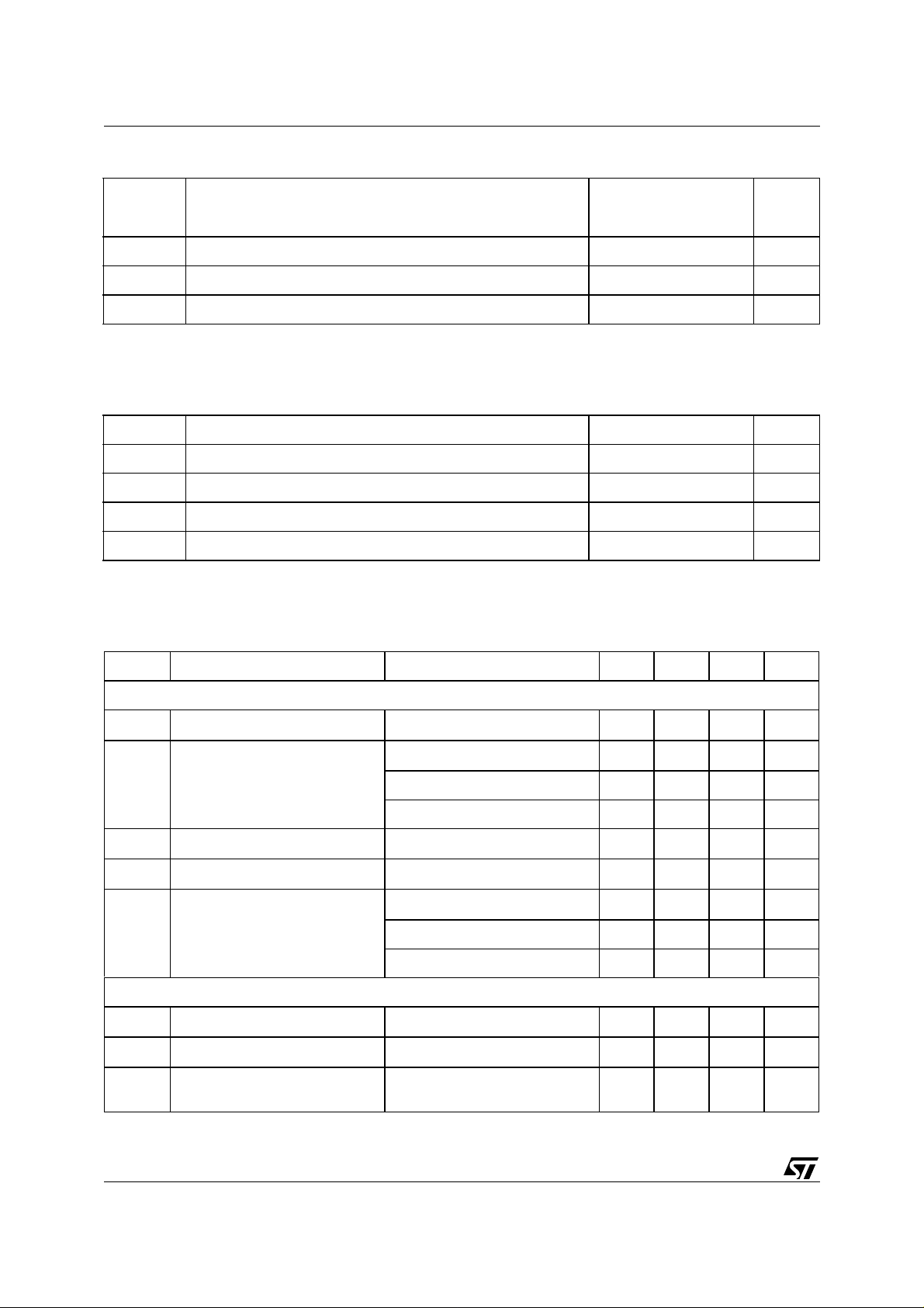
ELECTRICAL CHARACTERISTCS
All specifications are for 0<Tamb<70°C, VCC=12V, VDD=5V, unless otherwise noted.
Symbol Parameter Test Condition Min. Typ. Max. Unit
POWER SUPPLIES
12V supply 10.8 13.2 V
V
CC
I
VCC
V
rectified
V
I
THERMAL SENSING
T
T
Vcc Current SPINDLE + VCM TBD mA
SPINDLE ONLY TBD mA
VCM ONLY TBD mA
Vcc supply rectified 3.5 13.2 V
5V supply 4.5 5.5 V
dd
5V supply SPINDLE + VCM TBD mA
vdd
SPINDLE ONLY TBD mA
VCM ONLY TBD mA
SHUTDOWN TEMPERATURE 150 180 °C
SD
HYSTERESIS 60 °C
HYS
6/23
T
EARLY WARNING TSD-
EW
°C
25
Page 7
L7200
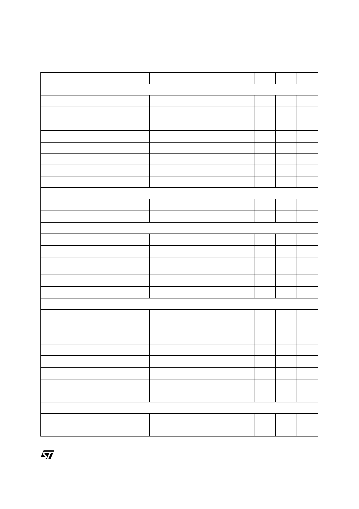
ELECTRICAL CHARACTERISTCS
(continued)
Symbol Parameter Test Condition Min. Typ. Max. Unit
SUPPLY MONITOR
V
V
R
on_por
T
PorDly
TRIP POINT 2.5V-3.3V-5V-12V INPUT RISING 1.20 1.25 1.30 V
TR
HYSTERESIS VOLTAGE INPUT FALLING 25 mV
HYS
PORB PULL DOWN Ron Vdd > 2V and sink 1mA 500 W
POR Delay Time 80 mSec
12VTR Minimum Voltage 12V 8.6 V
5VTR Minimum Voltage 5V 4.2 V
3.3VTR Minimum Voltage 3.3V 3.135 V
2.5VTR Minimum Voltage 2.5V 2.375 V
VOLTAGE BOOST
V
BOOST
F
OUTPUT VOLTAGE VCC+5
INTERNAL OSCI LLATOR 200 KHz
OSC
VCC+6.3
SW1 OUTPUT
V
INPUT LOGIC "1" 2.4 V
IH
V
V
V
INPUT LOGIC "0" 0.5 V
IL
OUTPUT LOGIC "1" ISOURCE = 20µAVdd-
OH
V
0.2
V
F
SYSCLK
OUTPUT LOGIC "0" ISOURCE = -400µA 0.4V
OL
SYSTEM CLOCK 20 25 MHz
VCM, DAC
RESOLUTION 14 BITS
DIFFERENTIAL LINEARITY 1 LSB Change
- Tested
- By design
-1
-0.5
1
0.5
INTEGRAL LINEARITY 9 BITS
MIDSCALE OFFSET REFERENCED TO V
CONVERTION TIME 5 µs
T
C
FULL SCALE VOLTAGE REFERENCED TO V
CC/4
CC/4
-5 5 mV
±1 V
FULL SCALE ERROR -6 6 %
VCM, ERROR AMPLIFIER
AVOL OPEN LOOP GAIN DC 80 dB
LSB
VOS INPUT OFFSET VOLTAGE 1 mV
7/23
Page 8

L7200
ELECTRICAL CHARACTERISTCS
(continued)
Symbol Parameter Test Condition Min. Typ. Max. Unit
VICM INPUT COMMON MODE
RANGE
VCC/4
+/-1.5
FODB UNITY GAIN BANDWIDTH 10 MHz
VCM, POWER STAGE
R
DS(ON)
I
I
O(LEAK)
Output On Resistance (Each
Device)
Operating Current 1.3 A
o
Output Leakage Current Vcc = 14V 1.0 mA
Tj = 25°C
T
= 125°C
j
0.25
0.35 Ω
VCM, CURRENT SENSE AMPLIFIER
A
Voltage Gain 3.88 4 4.12 V/V
V
V
Input Common Mode Range -0.3 Vcc
ICM
+0.3
V
V
F
OCM
Output Common Mode Range -1mA < Io < 1mA 1.5 4.5 V
Output Offset Voltage SENSE_IN(-/+) = Vcc/4 10 mV
OS
3dB Bandwidth 3 MHz
3dB
V
V
CMRR Input Common Mode Rejection
50 dB
Ratio
PSRR Power Supply Rejection Ratio 60 dB
VCM RETRACT
V
T
retract
Retract Voltage PKV=0 & PKV1=0 & PKV2=0
park
PKV=1 & PKV1=0 & PKV2=0
PKV=0 & PKV1=1 & PKV2=0
PKV=1 & PKV1=1 & PKV2=0
PKV=0 & PKV1=0 & PKV2=1
PKV=1 & PKV1=0 & PKV2=1
PKV=0 & PKV1=1 & PKV2=1
PKV=1 & PKV1=1 & PKV2=1
Retract Time
limited by the internal
oscillator 200KHz
RT0 = 0 & RT1 = 0
RT0 = 1 & RT1 = 0
RT0 = 0 & RT1 = 1
RT0 = 1 & RT1 = 1
0.30
0.60
0.90
1.20
1.50
1.80
2.10
2.40
80
160
320
640
SPINDLE, PWM CURRENT SENSE COMPARATOR
T
Delay to Fcom Out 200 500 ns
DLY
SPINDLE, POWER STAGE
R
DS(ON)
Output On Resistance (each
device)
Tj = 25°C
T
= 125°C
j
0.25
0.35
V
ms
Ω
I
O(LEAK)
8/23
Start-up Current 2A
I
o
Output Leakage Current VCC = 14V 1.0 mA
Page 9

L7200
ELECTRICAL CHARACTERISTCS
(continued)
Symbol Parameter Test Condition Min. Typ. Max. Unit
BEMF
N
V
HYS
Output Slew Rate (PWM) Reg# 2.2 = 0
Reg# 2.2 = 1
Minimum BEMF Voltage for
MI
Detection
Hysteresis 18 mV
10
20
35 mVp-p
CURRENT SENSE AMPLIFIER
A
Voltage Gain 3.8 4.0 4.2 V/V
v
/dt Output Slew Rate 20 V/µS
dV
o
3.3V LINEAR REGULATOR
V3.3 3.3V Regulation Voltage Iload < 0.6A 3.15 3.3 3.45 V
Av Open Loop Gain 60 dB
Ibase Driving Base Current 20 mA
2.5V LINEAR REGULATOR
V2.5 2.5V Regulation Voltage Iload < 0.6A 2.5 V
Av Open Loop Gain 60 dB
V/µs
Ibase Driving Base Current 20 mA
8V LINEAR REGULATOR
V
A
I
base
8V Regulation Voltage I
8
Open Loop Gain 60 dB
V
Driving Base Current 5 mA
< 0.2A 8 V
load
SHOCK SENSOR - INPUT OPERATIONAL AMPLIFIER A1
Av Open Loop Gain 20 dB
Rin Input Inpedance 10 MΩ
FodB Unity Gain Bandwidth 30 KHz
SHOCK SENSOR - FILTER OPERATIONAL AMPLIFIER A2
Av Open Loop Gain 80 dB
FodB Unity Gain Bandwidth 5 KHz
V
offset
Offset Voltage ±5 V
SHOCK SENSOR - OUTPUT WINDOW COMPARATOR
V
Vth High Referred to Vcc/4 +0.5 V
H
V
Vth Low Referred to Vcc/4 -0.5 V
L
9/23
Page 10

L7200
SERIAL PORT
PARAMETER MIN. TYP. MAX. UNITS
SCLK Period, (T
SCLK low time, (T
SCLK high time, (T
Enable to SCLK (T
SCLK to disable (T
Data set-up time before rising edge SCLK (T
Data hold time (T
Minimum SDEN low time (T
)25ns
SCK
)10ns
CKL
)10ns
CKH
)1015ns
SDENS
) 12.5 ns
SDENH
DS
)5ns
DH
)30ns
SDENL
Figure 1. Serial Port Ti min g In form ation
SDEN
SCLK
SDATA
0A0 A6A1D0 D1
1st Byte 2nd Byte
)5ns
D2 D7
Serial Port Write Timing
SDEN
SCLK
SDATA
1A0 A6A1D0 D1
1st Byte 2nd Byte
Serial Port Read Timing
D7
SERIAL PORT OPERATION
The serial port inter face is a bi-directi onal port for readi ng and writing pr ogramming data fr om/to the internal registers of this device. For data transfers SDEN is brought high, serial data is presented at the SDATA pin, and a
serial clock is applied to the SCLK pin. After the SDEN goes high , the first 16 pulses applied to the SCLK pin
will shift the data presented at the SDATA pin into an internal shift register on the rising edge of each clock. An
internal counter prevents more than 16 bits from being shifted into the register. The data in the shift register is
10/23
Page 11

L7200
latched after the 16th SC LK pulse. If less than 16 clock pulses are provided before SDEN goes low, the data
transfer is aborted.
All transfers are shifted into the serial port LSB first. The first byte of the transfer is for Address and Instruction
information. The first bit is R/W instruction bit, 0 is for WRITE and 1 is for READ. Following 3 bits are for
Combo Data Bank (all set to ‘1’). The last 4 bits are for Register Address.
Figure 2. Serial Port Data Transfer Format
SDEN
SCLK
SDATA
INSTRUCTION (READ/WRITE), 1BIT
ADDRESS, COMBO DATA BANK, 3 BITS
ADDRESS, 4 BITS
DATA, 8 BITS
INTERNAL REGISTERS DEFINITION
Reg: 0
Name: Spindle Spin-Up Register
Type: Write only
Address: 0Eh
BIT LABEL DESCRIPTION
0 START “0” Reset and Brakes the Spindle. “1” Initiates the Spindle Start-Up
procedure.
1 EXTERNAL “0” Spindle BEMF processing in internal mode. “1” External mode.
2 SEQINC In external mode, a “0” to ”1” transition, increments the Spindle
Sequencer.
3 STOP “0” Complete Internal Spindle Start-Up. “1” Stop after Inductive Sense
4 INDSENSE “0” Normal condition. “1” in External mode, initiate the Inductive
Sense
5 SPCOAST “0” Spindle Outputs Enabled. “1” Disabled.
6 SPINUPTIME 0 Spindle Internal Spin Up.
Energization Time. First Bit. 0 0 10mS
7 SPINUPTIME 1 Spindle Internal Spin Up. 0 1 20mS
Energization Time. Second Bit. 1 0 30mS
Bit 7 Bit 6 Time
1 1 40mS
11/23
Page 12

L7200
INTERNAL REGISTERS DEFINITION
(continued)
Reg: 1
Name: Spindle Set-Up 0 Register
Type: Write only
Address: 1Eh
BIT LABEL DESCRIPTION
0 SMOOTH “0” Spindle SMOOTHDRIVE™. “1” Spindle Six step drive.
1 BIPMASK Spindle Mask Time. “0” 15°. “1” 7.5°. (Only in six step drive).
2 MINON 0 Minimum ON time in Current
limit. First Bit. 0 0 6µS
3 MINON 1 Minimum ON time in Current 0 1 3µS
limit. Second Bit. 1 0 9µS
4 BIPDELAY Spindle Commutation Delay. “0” 30°. “1” 15°. (Only in six step drive).
5 MASKSPIN 0 Spindle Mask at acceleration.
First Bit. 0 0 3.2mS
Bit 3 Bit 2 Min TON
11 7.6µS
Bit 6 Bit 5 Mask
6 MASKSPIN 1 Spindle Mask at acceleration. 0 1 1.6mS
Second Bit. 1 0 0.8mS
1 1 6.4mS
7 FREEZE “0” Torque Optimizer Activated. “1” Torque Optimizer Frozen.
Reg: 2
Name: Spindle Set-Up 1 Register
Type: Write only
Address: 2Eh
BIT LABEL DESCRIPTION
0 IL0 Current Limit and Inductive
Sense thresholds. First Bit. 0 0 0.45V
1 IL1 Current Limit and Inductive 0 1 0.50V
Sense thresholds. Second Bit. 1 0 0.55V
2 SSLEW Spindle Chopping Slew Rate. “0” 10V/µS. “1” 20V/µS.
Bit 1 Bit 0 Vlimit
1 1 0.75V
3 FLLEXT Spindle Speed control loop. “0” Internal. “1” External.
12/23
Page 13

L7200
INTERNAL REGISTERS DEFINITION
BIT LABEL DESCRIPTION
4 INDEX External FLL update.
5 EXTK “0” Spindle Speed internal KFLL. “1” All Reg#7 and Lsb of Reg#8 bits are
6 MECH/ELEC Electrical or Mechanical cycle for Spindle FLL control.
7 8_12POLE Spindle Motor Poles. “0” 8 poles. “1” 12 poles.
(continued)
mixed to allow external setting of KFLL.
“0” Mechanical. “1” Electrical.
Reg: 3
Name: Spindle Set-Up 2 Register
Type: Write only
Address: 3Eh
BIT LABEL DESCRIPTION
0 ZCWINDOW Chop cycle for Spindle ZC tristate time. “0” Two. “1” One.
1 REVBRAKE “1” Spindle Reverse Brake. Toggling this bit will define the time before
ending over normal brake. 1 = 10mS. 2 = 20mS. 3 = 40mS.
2 CLKDIV SYSCLK divider. “0” SYSCLK. “1” SYSCLK divide by 2.
3 DIV1.5 SYSCLK divider. “0” SYSCLK. “1” SYSCLK divide by 1.5.
4 FLLCOARSE<0> LSB of Spindle FLL Coarse Counter.
5 FLLCOARSE<1> Bit 1 of Spindle FLL Coarse Counter.
6 FLLCOARSE<2> Bit 2 of Spindle FLL Coarse Counter.
7 FLLCOARSE<3> Bit 3 of Spindle FLL Coarse Counter.
Reg: 4
Name: Spindle FLL Coarse Register
Type: Write only
Address: 4Eh
BIT LABEL DESCRIPTION
0 FLLCOARSE<4> Bit 4 of Spindle FLL Coarse Counter.
1 FLLCOARSE<5> Bit 5 of Spindle FLL Coarse Counter.
2 FLLCOARSE<6> Bit 6 of Spindle FLL Coarse Counter.
3 FLLCOARSE<7> Bit 7 of Spindle FLL Coarse Counter.
4 FLLCOARSE<8> Bit 8 of Spindle FLL Coarse Counter.
5 FLLCOARSE<9> Bit 9 of Spindle FLL Coarse Counter.
13/23
Page 14

L7200
INTERNAL REGISTERS DEFINITION
BIT LABEL DESCRIPTION
6 FLLCOARSE<10> Bit 10 of Spindle FLL Coarse Counter.
7 FLLCOARSE<11> MSB of Spindle FLL Coarse Counter.
(continued)
Reg: 5
Name: Spindle FLL Fine Register
Type: Write only
Address: 5Eh
BIT LABEL DESCRIPTION
0 FLLFINE<0> LSB of Spindle FLL Fine Counter.
1 FLLFINE<1> Bit 1 of Spindle FLL Fine Counter.
2 FLLFINE<2> Bit 2 of Spindle FLL Fine Counter.
3 FLLFINE<3> Bit 3 of Spindle FLL Fine Counter.
4 FLLFINE<4> Bit 4 of Spindle FLL Fine Counter.
5 FLLFINE<5> Bit 5 of Spindle FLL Fine Counter.
6 FLLFINE<6> Bit 6 of Spindle FLL Fine Counter.
7 FLLFINE<7> Bit 7 of Spindle FLL Fine Counter.
Reg: 6
Name: Spindle Set-Up 3 Register
Type: Write only
Address: 6Eh
BIT LABEL DESCRIPTION
0 FLLFINE<8> Bit 8 of Spindle FLL Fine Counter.
1 FLLFINE<9> Bit 9 of Spindle FLL Fine Counter.
2 FLLFINE<10> MSB of Spindle FLL Fine Counter.
3 COEFF_B0<8> MSB of Spindle FLL filter coefficient B0.
4 COEFF_B1<8> MSB of Spindle FLL filter coefficient B1.
5 STUCKSET Spindle Stuck Rotor Time. “0” 400mS. “1” 100mS.
6 CLAMP0 KFLL clamp. First Bit.
7 CLAMP1 KFLL clamp. Second Bit. 0 0 0.50
Bit 7 Bit 6 Clamp
010.55
14/23
100.60
110.65
Page 15

L7200
INTERNAL REGISTERS DEFINITION
(continued)
Reg: 7
Name: Spindle FLL Filter Coefficient A1 Register
Type: Write only
Address: 7Eh
BIT LABEL DESCRIPTION
0 COEFF_A1<0> LSB of Spindle FLL filter coefficient A1.
1 COEFF_A1<1> Bit 1 of Spindle FLL filter coefficient A1.
2 COEFF_A1<2> Bit 2 of Spindle FLL filter coefficient A1.
3 COEFF_A1<3> Bit 3 of Spindle FLL filter coefficient A1.
4 COEFF_A1<4> Bit 4 of Spindle FLL filter coefficient A1.
5 COEFF_A1<5> Bit 5 of Spindle FLL filter coefficient A1.
6 COEFF_A1<6> Bit 6 of Spindle FLL filter coefficient A1.
7 COEFF_A1<7> MSB of Spindle FLL filter coefficient A1.
Reg: 8
Name: Spindle FLL Filter Coefficient B0 Register
Type: Write only
Address: 8Eh
BIT LABEL DESCRIPTION
0 COEFF_B0<0> LSB of Spindle FLL filter coefficient B0.
1 COEFF_B0<1> Bit 1 of Spindle FLL filter coefficient B0.
2 COEFF_B0<2> Bit 2 of Spindle FLL filter coefficient B0.
3 COEFF_B0<3> Bit 3 of Spindle FLL filter coefficient B0.
4 COEFF_B0<4> Bit 4 of Spindle FLL filter coefficient B0.
5 COEFF_B0<5> Bit 5 of Spindle FLL filter coefficient B0.
6 COEFF_B0<6> Bit 6 of Spindle FLL filter coefficient B0.
7 COEFF_B0<7> Bit 7 of Spindle FLL filter coefficient B0.
15/23
Page 16

L7200
INTERNAL REGISTERS DEFINITION
(continued)
Reg: 9
Name: Spindle FLL Filter Coefficient B1 Register
Type: Write only
Address: 9Eh
BIT LABEL DESCRIPTION
0 COEFF_B1<0> LSB of Spindle FLL filter coefficient B1.
1 COEFF_B1<1> Bit 1 of Spindle FLL filter coefficient B1.
2 COEFF_B1<2> Bit 2 of Spindle FLL filter coefficient B1.
3 COEFF_B1<3> Bit 3 of Spindle FLL filter coefficient B1.
4 COEFF_B1<4> Bit 4 of Spindle FLL filter coefficient B1.
5 COEFF_B1<5> Bit 5 of Spindle FLL filter coefficient B1.
6 COEFF_B1<6> Bit 6 of Spindle FLL filter coefficient B1.
7 COEFF_B1<7> Bit 7 of Spindle FLL filter coefficient B1.
Reg: 10
Name: Voice Coil DAC 0 Register
Type: Write only
Address: AEh
BIT LABEL DESCRIPTION
0 VCMDAC<0> LSB of Voice Coil DAC.
1 VCMDAC<1> Bit 1 of Voice Coil DAC.
2 VCMDAC<2> Bit 2 of Voice Coil DAC.
3 VCMDAC<3> Bit 3 of Voice Coil DAC.
4 VCMDAC<4> Bit 4 of Voice Coil DAC.
5 VCMDAC<5> Bit 5 of Voice Coil DAC.
6 VCMDAC<6> Bit 6 of Voice Coil DAC.
7 VCMDAC<7> Bit 7 of Voice Coil DAC.
16/23
Page 17

L7200
INTERNAL REGISTERS DEFINITION
(continued)
Reg: 11
Name: Voice Coil DAC 1 Register
Type: Write only
Address: BEh
BIT LABEL DESCRIPTION
0 VCMDAC<8> Bit 8 of Voice Coil DAC.
1 VCMDAC<9> Bit 9 of Voice Coil DAC.
2 VCMDAC<10> Bit 10 of Voice Coil DAC.
3 VCMDAC<11> Bit 11 of Voice Coil DAC.
4 VCMDAC<12> Bit 12 of Voice Coil DAC.
5 VCMDAC<13> MSB of Voice Coil DAC.
6 PSM/LIN VCM Current control. “0” Linear mode. “1” PSM mode.
7 VCMEN “0” VCM Disabled. “1” VCM Enabled.
Reg: 12
Name: Voice Coil Retract Register
Type: Write only
Address: CEh
BIT LABEL DESCRIPTION
0 PKV0 Retract Voltage. First Bit.
1 PKV1 Retract Voltage. Second Bit. 0 0 0 0.30V
2 PKV2 Retract Voltage. Third Bit. 0 0 1 0.60V
1001.50V
1011.80V
3 RT0 Retract Time. First Bit.
4 RT1 Retract Time. Second Bit. 0 0 80ms
Bit 2 Bit 1 Bit 0 Voltage
0100.90V
0111.20V
1102.10V
1112.40V
Bit 4 Bit 3 Time
0 1 160ms
1 0 320ms
1 1 640ms
17/23
Page 18

L7200
INTERNAL REGISTERS DEFINITION
BIT LABE L DESCRIPTION
5 RETDIR Retract Direction.
6 RETRACT “1” Retracts the Voice Coil arm.
7 RETBRK “1” Brakes the VCM for the first 20mS of the retract time then it reverses
(continued)
“0” VCM- high, VCM+ low. “1” VCM- low, VCM+ high.
the direction of the retract opposite to the RETDIR bit setting for other
20mS, then it finish the normal retract. This total 40mS are
subtructed from the programmed Retract time.
Reg: 13
Name: Voice Coil Set-Up and Ramp Loading Register
Type: Write only
Address: DEh
BIT LABEL DESCRIPTION
0 VCMCAL0 VCM Calibration. First Bit.
1 VCMCAL1 VCM Calibration. Second Bit. 0 0 0 0 None
2 VCMCAL2 VCM Calibration. Third Bit. 0 0 0 1 1.4mV
Bit 3 Bit2 Bit 1 Bit 0 Adj
3 VCMCAL3 VCM Calibration. Fourth Bit. 0 0 1 0 2.8mV
00114.2mV
01005.6mV
01017.0mV
01108.4mV
01119.8mV
100011.2mV
100112.6mV
101014.0mV
101115.4mV
110016.8mV
110118.2mV
111019.6mV
111121.0mV
4 VCMCALDIR VCM Calibration Direction. “0” Positive offset. “1” Negative offset.
5 RAMPLOADING VCM Ramp Loading Setting. “1” Ramp Loading mode.
6 SAMPLE/HOLD VCM Ramp Loading Setting. “0” Hold. “1” Sampling.
7 TRISTATE VCM Ramp Loading Setting. “1” Synchronusly clamps the VCM outputs until
current is less than 100mA, then tristate them.
18/23
Page 19

L7200
INTERNAL REGISTERS DEFINITION
(continued)
Reg: 14
Name: System FunctionSet-Up Register
Type: Write only
Address: EEh
BIT LABEL DESCRIPTION
0 GAINSWITCH VCM current loop Gain Switch. “0” Switch open. “1” Switch close.
1 EXTP VCM external mode VCMP output. “0” VCMP low. “1” VCMP high.
2 EXTN VCM external mode VCMN output. “0” VCMN low. “1” VCMN high.
3 EXTVCM VCM mode. “0” Internal. “1” External.
4 VBDIS Vboost oscillatotor. “0” Enabled. “1” Disabled.
5 SHOCKEN Schock Detector. “0” Disabled. “1” Enabled.
6
7
Reg: 15
Name: Spindle Diagnostic Register
Type: Read only
Address: 0Fh
BIT LABEL DESCRIPTION
0 LOCK “0” Indicates Spindle Speed error (>16µS sample, either mechanical or
electrical).
1 NOTHR “1” Indicates that the Inductive Sense threshold is not reached.
2 PHREADY “1” Indicates that the Phase reading of the motor succeded.
3 STUCKROTOR “1” Indicates that the Spindle BEMF is not detected.
4 PHASE<0> Inductive Sense Phase detected. First Bit.
5 PHASE<1> Inductive Sense Phase detected. Second Bit.
6 PHASE<2> Inductive Sense Phase detected. Third Bit.
7 BACKSPIN “1” Indicateds a Back rotation of the Spindle Motor.
19/23
Page 20

L7200
INTERNAL REGISTERS DEFINITION
(continued)
Reg: 16
Name: System Diagnostic Register
Type: Read only
Address: 1Fh
BIT LABEL DESCRIPTION
0 PHASEFINE<0> Torque Optimizer Phase Shift. First Bit.
1 PHASEFINE<1> Torque Optimizer Phase Shift. Second Bit.
2 PHASEFINE<2> Torque Optimizer Phase Shift. Third Bit.
3 PHASEFINE<3> Torque Optimizer Phase Shift. Fourth Bit.
4 THWARNING Thermal Warning. “1” Indicates that the Device temperature is
approximately 25°C lower than the thermal shutdown’s one.
5 THSHUTDOWN Thermal Shutdown. “1” Indicates that the Device temperature has
exceeded 160°C. The bit will reset (=0) when the temperature drops
below 130°C.
6 VCMCAL Outputs of the Calibration Comparator.
7 RET “1” Indicates that the Voicel Coil is Retracting.
Reg: 17
Name: ID Register
Type: Read only
Address: 2Fh
BIT LABEL DESCRIPTION
0 ID_REV0 Device Minor Revision. First Bit.
1 ID_REV1 Device Minor Revision. Second Bit.
2 ID_REV2 Device Minor Revision. Third Bit.
3 ID_REV3 Device Minor Revision. Fourth Bit.
4 ID_REV4 Device Major Revision. First Bit.
5 ID_REV5 Device Major Revision. Second Bit.
6 ID_REV6 Device Major Revision. Third Bit.
7 ID_REV7 Device Major Revision. Fourth Bit.
20/23
Page 21

APPLICATION CIRCUIT
L7200
VCC
SYSCLK
SDEN
SDATA
SCLK
FCOM
PORB
SENSOR OUT
SENSOR IN
33nF
22uF/25V
Tantalum
330pF
CTAPOUT_COUT_BOUT_A
2.2uF
25
1
2
47
+
48
40
6
41
42
43
7
31
15
10K
19
18
17
5V
63
64
59
60
55
56
5
44
24
8
9
VDD
BRAKE
AVCC
VCC
VCC
VCC
VCC
DGND
SYSCLK
SDEN
SDATA
SCLK
FCOM
PORB
SSOUT
SSIN
SSBUFOUT
SSFIN
SSFOUT
VBOOST
161314515253543536495023222120
GND
GND
AGND
OUT_A
OUT_A
"MOZART"
TQFP64
PUMP
VCM_GND
VCM_GND
VCM_A-
VCM_A-
OUT_B
OUT_B
OUT_C
SENSE_IN-
SENSE_IN+
VCM_A+
OUT_C
VCM_A+
62
11
CTAP
TR_12V
RSENSE
TR_5V
0.3ohm / 1W
57
58
61
RSENSE
RSENSE
RSENSE
ISENSE
VREG8_DRV
VREG8_IN
VREG3.3_DRV
VREG3.3_IN
VREG2.5_DRV
VREG2.5_IN
GAINRES
DAC_OUT
ERROR_IN
ERROR_OUT
SENSE_OUT
TR_3.3V
TR_2.5V
RBIAS
26
VPS
VPS
VPS
VPS
12V
12V
12V
12K
60K
1nF
10K
PNP
10uF
5V
PNP
10uF
5V
PNP
10uF
10
33
34
3
4
29
30
46
45
27
28
12
32
39
62K
38
37
100K
1N4148
1uF
Analog Ground Power Ground VCM Ground Digital Ground
47nF
1N4148
VCC
0.25ohm
1W
VCM_A+VCM_A-
21.5K
21/23
Page 22

L7200
DIM.
mm inch
MIN. TYP. MAX. MIN. TYP. MAX.
A 1.60 0.063
A1 0.05 0.15 0.002 0.006
A2 1.35 1.40 1.45 0.053 0.055 0.057
B 0.18 0.23 0.28 0.007 0.009 0.011
C 0.12 0.16 0.20 0.0047 0.0063 0.0079
D 12.00 0.472
D1 10.00 0.394
D3 7.50 0.295
e 0.50 0.0197
E 12.00 0.472
E1 10.00 0.394
E3 7.50 0.295
L 0.40 0.60 0.75 0.0157 0.0236 0.0295
L1 1.00 0.0393
K 0°(min.), 7°(max.)
OUTLINE AND
MECHANICAL DATA
TQFP64
D
D1
TQFP64
3348
32
E3D3E1
17
16
E
L1
L
0.10mm
Seating Plane
K
49
B
64
1
e
A1
B
A
A2
C
22/23
Page 23

L7200
Information furnished is believed to be accurate and reliable. However, STMicroelectronics assumes no responsibility for the consequences
of use of such information nor for any infringement of patents or other rights of third parties which may result from its use. No license is granted
by implic ation or otherwise under any patent or p at ent rights of STMicroelectronics. Spec i fications mentioned i n this publication are subject
to change without notice. This publication supersedes and replaces all information previously supplied. STMicroelectronics products are not
authorized for use as cri t i cal compone nts in life support device s or systems without express written approval of STMicroel ectronics.
The ST logo is a registered trademark of STMicroelectronics
1999 STMi croelectronics - All Ri ghts Rese rved
Australi a - Brazil - Chin a - Finland - Franc e - Germany - Hong Kong - India - Ita l y - Japan - Malaysi a - Malta - Morocco - Singapore - Spain
STMicroelectronics GROUP OF COMPANIES
- Sweden - Sw itzerlan d - United Kin gdom - U.S.A.
http://www.s t. com
23/23
 Loading...