

Page 1
Adjustable step-down controller with synchronous rectification
Features
■ Input voltage range from 1.8 V to 14 V
■ Supply voltage range from 4.5 V to 14 V
■ Adjustable output voltage down to 0.6 V with
±0.8% accuracy over line voltage and
temperature (0°C~125°C)
■ Fixed frequency voltage mode control
■ t
■ 0% to 100% duty cycle
■ Selectable 0.6 V or 1.2 V internal voltage
■ External input voltage reference
■ Soft-start and inhibit
■ High current embedded drivers
■ Predictive anti-cross conduction control
■ Selectable uvlo threshold (5 V or 12 V BUS)
■ Programmable high-side and low-side R
■ Switching frequency programmable
■ Master/slave synchronization with 180° phase
■ Pre-bias start up capability (L6730)
■ Selectable source/sink or source only
■ Selectable constant current or hiccup mode
■ Power Good output with programmable delay
■ Overvoltage protection with selectable
■ Thermal shut-down
■ Package: HTSSOP20
lower than 100 ns
ON
reference
sense overcurrent protection
DS(on)
from 100 kHz to 1 MHz
shift
capability after soft-start (L6730)
overcurrent protection after soft-start (L6730B)
latched/not-latched mode
HTSSOP20
Applications
■ High performance / high density DC-DC
modules
■ Low voltage distributed DC-DC
■ niPOL converters
■ DDR memory supply
■ DDR memory bus termination supply
Table 1. Device summary
Order codes Package Packing
L6730 HTSSOP20 Tube
L6730TR HTSSOP20 Tape and reel
L6730B HTSSOP20 Tube
L6730BTR HTSSOP20 Tape and reel
L6730
L6730B
December 2009 Doc ID 11938 Rev 3 1/52
www.st.com
52
Page 2

Contents L6730 - L6730B
Contents
1 Summary description . . . . . . . . . . . . . . . . . . . . . . . . . . . . . . . . . . . . . . . . 4
1.1 Functional description . . . . . . . . . . . . . . . . . . . . . . . . . . . . . . . . . . . . . . . . 5
1.2 Application circuit . . . . . . . . . . . . . . . . . . . . . . . . . . . . . . . . . . . . . . . . . . . . 6
2 Electrical data . . . . . . . . . . . . . . . . . . . . . . . . . . . . . . . . . . . . . . . . . . . . . . 7
2.1 Maximum rating . . . . . . . . . . . . . . . . . . . . . . . . . . . . . . . . . . . . . . . . . . . . . 7
2.2 Thermal data . . . . . . . . . . . . . . . . . . . . . . . . . . . . . . . . . . . . . . . . . . . . . . . 7
3 Pin connections and functions . . . . . . . . . . . . . . . . . . . . . . . . . . . . . . . . 8
4 Electrical characteristics . . . . . . . . . . . . . . . . . . . . . . . . . . . . . . . . . . . . 11
5 Device description . . . . . . . . . . . . . . . . . . . . . . . . . . . . . . . . . . . . . . . . . 14
5.1 Oscillator . . . . . . . . . . . . . . . . . . . . . . . . . . . . . . . . . . . . . . . . . . . . . . . . . 14
5.2 Internal LDO . . . . . . . . . . . . . . . . . . . . . . . . . . . . . . . . . . . . . . . . . . . . . . . 15
5.3 Bypassing the LDO to avoid the voltage drop with low Vcc . . . . . . . . . . . 15
5.4 Internal and external references . . . . . . . . . . . . . . . . . . . . . . . . . . . . . . . . 16
5.5 Error amplifier . . . . . . . . . . . . . . . . . . . . . . . . . . . . . . . . . . . . . . . . . . . . . . 17
5.6 Soft-start . . . . . . . . . . . . . . . . . . . . . . . . . . . . . . . . . . . . . . . . . . . . . . . . . . 17
5.7 Driver section . . . . . . . . . . . . . . . . . . . . . . . . . . . . . . . . . . . . . . . . . . . . . . 20
5.8 Monitoring and protection . . . . . . . . . . . . . . . . . . . . . . . . . . . . . . . . . . . . . 21
5.9 Adjustable masking time . . . . . . . . . . . . . . . . . . . . . . . . . . . . . . . . . . . . . 27
5.10 Multifunction pin (S/O/U L6730) (CC/O/U L6730B) . . . . . . . . . . . . . . . . . 27
5.11 Synchronization . . . . . . . . . . . . . . . . . . . . . . . . . . . . . . . . . . . . . . . . . . . . 28
5.12 Thermal shutdown . . . . . . . . . . . . . . . . . . . . . . . . . . . . . . . . . . . . . . . . . . 29
5.13 Minimum ON-time TON(MIN) . . . . . . . . . . . . . . . . . . . . . . . . . . . . . . . . . . 29
5.14 Bootstrap anti-discharging system . . . . . . . . . . . . . . . . . . . . . . . . . . . . . . 30
5.14.1 Fan power supply failure . . . . . . . . . . . . . . . . . . . . . . . . . . . . . . . . . . . . 31
5.14.2 No-sink at zero current operation . . . . . . . . . . . . . . . . . . . . . . . . . . . . . . 31
6 Application details . . . . . . . . . . . . . . . . . . . . . . . . . . . . . . . . . . . . . . . . . 33
6.1 Inductor design . . . . . . . . . . . . . . . . . . . . . . . . . . . . . . . . . . . . . . . . . . . . . 33
2/52 Doc ID 11938 Rev 3
Page 3

L6730 - L6730B Contents
6.2 Output capacitors . . . . . . . . . . . . . . . . . . . . . . . . . . . . . . . . . . . . . . . . . . . 34
6.3 Input capacitors . . . . . . . . . . . . . . . . . . . . . . . . . . . . . . . . . . . . . . . . . . . . 34
6.4 Compensation network . . . . . . . . . . . . . . . . . . . . . . . . . . . . . . . . . . . . . . 35
6.5 Two quadrant or one quadrant operation mode (L6730) . . . . . . . . . . . . . 37
7 L6730 demonstration board . . . . . . . . . . . . . . . . . . . . . . . . . . . . . . . . . . 38
7.1 Description . . . . . . . . . . . . . . . . . . . . . . . . . . . . . . . . . . . . . . . . . . . . . . . . 38
7.2 PCB layout . . . . . . . . . . . . . . . . . . . . . . . . . . . . . . . . . . . . . . . . . . . . . . . . 39
8 I/O Description . . . . . . . . . . . . . . . . . . . . . . . . . . . . . . . . . . . . . . . . . . . . . 43
9 Efficiency . . . . . . . . . . . . . . . . . . . . . . . . . . . . . . . . . . . . . . . . . . . . . . . . . 45
10 POL demonstration board . . . . . . . . . . . . . . . . . . . . . . . . . . . . . . . . . . . 47
10.1 Description . . . . . . . . . . . . . . . . . . . . . . . . . . . . . . . . . . . . . . . . . . . . . . . . 47
11 Package mechanical data . . . . . . . . . . . . . . . . . . . . . . . . . . . . . . . . . . . . 49
12 Revision history . . . . . . . . . . . . . . . . . . . . . . . . . . . . . . . . . . . . . . . . . . . 51
Doc ID 11938 Rev 3 3/52
Page 4

Summary description L6730 - L6730B
1 Summary description
The controller is an integrated circuit designed using BiCMOS-DMOS, v5 (BCD5)
technology that provides complete control logic and protection for high performance, stepdown DC/DC and niPOL converters.
It is designed to drive N-Channel MOSFETs in a synchronous rectified buck converter
topology. The output voltage of the converter can be precisely regulated down to 600 mV,
with a maximum tolerance of ±0.8%, or to 1.2 V, when one of the internal references is used.
It is also possible to use an external reference from 0 V to 2.5 V.
The input voltage can range from 1.8 V to 14 V, while the supply voltage can range from 4.5
V to 14 V. High peak current gate drivers provide for fast switching to the external power
section and the output current can be in excess of 20 A, depending on the number of the
external MOSFETs used. The PWM duty cycle can range from 0% to 100% with a minimum
on-time (T
very high switching frequency possible.
The device provides voltage-mode control. It includes a 400 kHz free-running oscillator that
is adjustable from 100 kHz to 1 MHz. The error amplifier features a 10 MHz gain-bandwidthproduct and 5 V/µs slew-rate that permits to realize high converter bandwidth for fast
transient response. The device monitors the current by using the R
side and low-side MOSFET(s), eliminating the need for a current sensing resistor and
guaranteeing an effective over current-protection in all the application conditions. When
necessary, two different current limit protections can be externally set through two external
resistors. A leading edge adjustable blanking time is also available to avoid false overcurrent-protection (OCP) intervention in every application condition.
ON(MIN)
) lower than 100 ns, making conversions with a very low duty cycle and
of both the high-
DS(ON)
It is possible to select the HICCUP mode or the constant current protection (L6730B) after
the soft-start phase.
During this phase constant current protection is provided. It is possible to select the sinksource or the source-only mode capability (before the device powers on) by acting on a
multifunction pin (L6730). The L6730 disables the sink mode capability during the soft-start
in order to allow a proper start-up also in pre-biased output voltage conditions. The L6730B
can always sink current and, so it can be used to supply the DDR memory BUS termination.
Other features include Master-Slave synchronization (with 180° phase shift), Power-Good
with adjustable delay, over voltage-protection, feed back disconnection, selectable UVLO
threshold (5 V and 12 V Bus), and thermal shutdown. The HTSSOP20 package allows the
realization for very compact DC/DC converters.
4/52 Doc ID 11938 Rev 3
Page 5
L6730 - L6730B Summary description
1.1 Functional description
Figure 1. Block diagram
VCC=4.5V to14V
V
=1.8V to14V
in
OCL
PGOOD
OCH
LDO
VCCDR
BOOT
Monitor
SS/INH
SYNCH
OSC
EAREF
PGOOD
SINK/OVP/UVLO*
TMASK
Protection
and Ref
+
-
MASKING TIME
ADJUSTMENT
OSC
L6730/B
0.6V
1.2V
-
+
PWM
E/A
+
-
FB
HGATE
PHASE
LGATE
PGND
GND
COMP
Note: In the L6730B the multifunction pin is: CC/OVP/UVLO.
Vo
Doc ID 11938 Rev 3 5/52
Page 6
Summary description L6730 - L6730B
1.2 Application circuit
Figure 2. Application circuit
VCC = 4.5V to 14V
DEC
THERMAL PAD
FB
R
OS
OCH
VCCDR
BOOT
HGATE
PHASE
LGATE
PGND
OCL
R
FILT
R
OCH
C
OCH
R
BOOT
C
BOOT
C
VCCDR
R
OCL
C
OCL
R
FB
RSC
S
VCCDR
R
R
SYNCH
R
H_SOU
H_OSC
L_OSCRL_SOU
SHORT PIN
R
R
H_MASK
L_MASK
1
C
VCC
GND
SYNCH
SS/INH
PGOOD DELAY
C
C
PGdelay
SS
L6730
R
PG
R
R
H_EAREF
L_EAREF
PGOOD
OSC
SOU/COU
TMASK
EAREF
C
EAREF
COMP
RFC
F
C
P
NOTE 1: In module application it is recommended to place the short pin on the module where device is mounted.
VCCDR
VIN = 1.8V to 14V
C
IN_BULK
C
R
HS
IN_HF
HS
LVout
R
LS
R
SN
LS
C
SN
C
OUT
6/52 Doc ID 11938 Rev 3
Page 7
L6730 - L6730B Electrical data
2 Electrical data
2.1 Maximum rating
Table 2. Absolute maximum ratings
Symbol Parameter Value Unit
V
VCC to GND and PGND, OCH, PGOOD
CC
V
BOOT - VPHASE
V
HGATE - VPHASE
V
BOOT
V
PHASE
Boot voltage 0 to 6 V
BOOT -0.3 to 24 V
PHASE -1 to 18
PHASE spike, transient < 50ns (F
= 500kHz)
SW
-0.3 to 18 V
0 to V
BOOT
- V
-3
+24
PHASE
V
V
SS, FB, EAREF, SYNC, OSC, OCL, LGATE, COMP,
S/O/U, TMASK, PGOODELAY, V
OCH Pin
Maximum withstanding voltage range
test condition: CDF-AEC-Q100-002 “human body
OTHER PINS ±2000
model” acceptance criteria: “normal performance”
2.2 Thermal data
Table 3. Thermal data
Symbol Description Value Unit
(1)
R
thJA
T
STG
T
J
T
A
1. Package mounted on demonstration board
Max. thermal resistance junction to ambient 50 °C/W
Storage temperature range -40 to +150 °C
Junction operating temperature range -40 to +125 °C
Ambient operating temperature range -40 to +85 °C
CCDR
-0.3 to 6 V
±1500
VPGOOD Pin ±1000
Doc ID 11938 Rev 3 7/52
Page 8
Pin connections and functions L6730 - L6730B
(
⋅
=
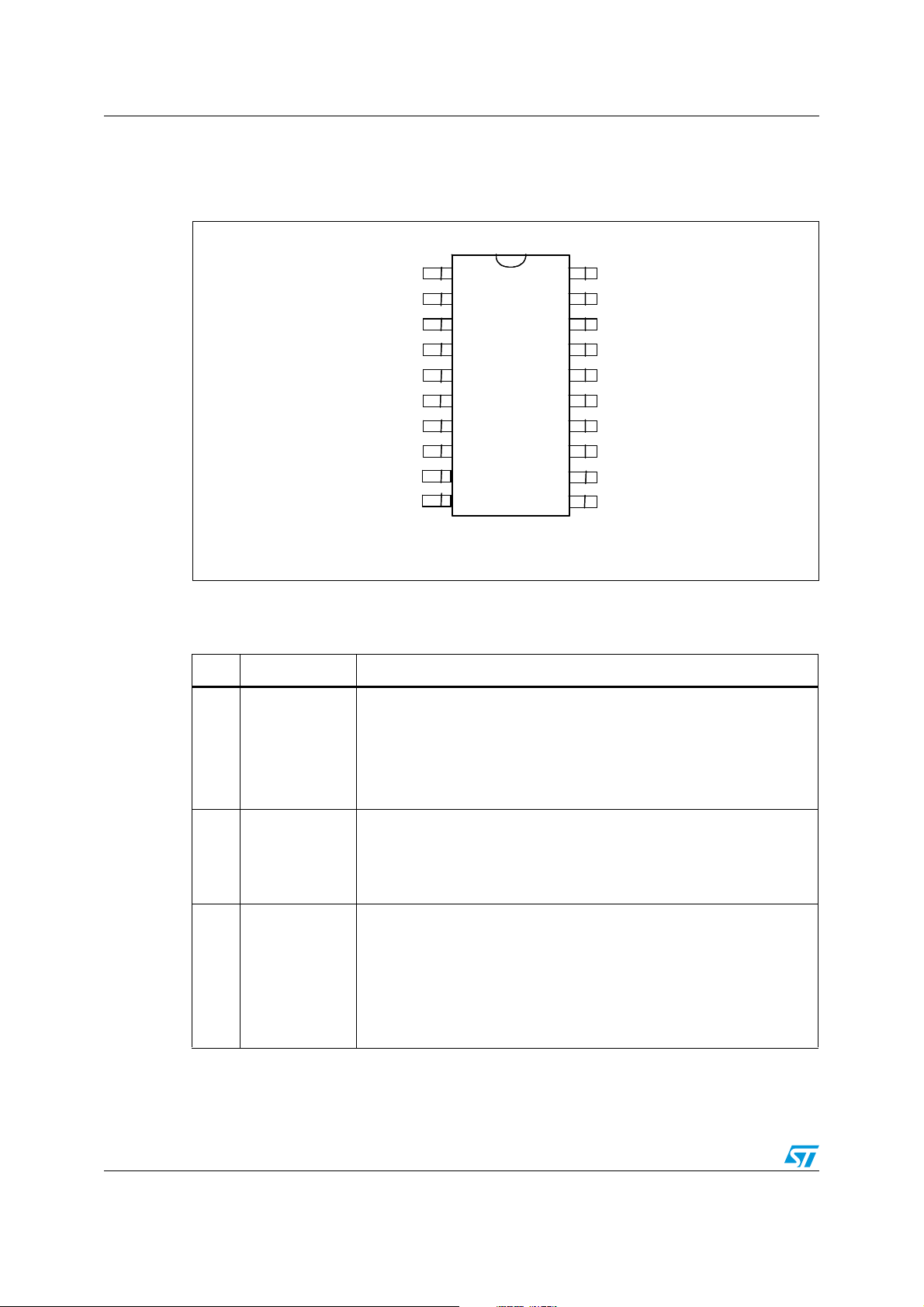
3 Pin connections and functions
Figure 3. Pins connection (top view)
PGOOD DELAY
PGOOD DELAY
SYNCH
SYNCH
SINK/OVP/UVLO
TMASK
TMASK
GND
GND
FB
FB
COMP
COMP
SS/INH
SS/INH
EAREF
EAREF
OSC
OSC
1
1
2
2
3
3
4
4
5
5
6
6
7
7
8
8
9
9
10
10
HTSSOP20
HTSSOP20
20
20
19
19
18
18
17
17
16
16
15
15
14
14
13
13
12
12
11
11
Note: In the L6730B the multifunction pin is: CC/OVP/UVLO.
Table 4. Pin connection
Pin n. Name Description
A capacitor connected between this pin and GND introduces a delay
between the internal PGOOD comparator trigger and the external signal
1 PGOOD DELAY
rising edge. No delay can be introduced on the falling edge of the
PGOOD signal. The delay can be calculated with the following formula:
PGOOD
PGOOD
VCC
VCC
VCCDR
VCCDR
LGATE
LGATE
PGND
PGND
BOOT
BOOT
HGATE
HGATE
PHASE
PHASE
OCH
OCH
OCL
OCL
Two or more devices can be synchronized by connecting the SYNCH pins
together. The device operating with the highest F
2 SYNCH
device. The Slave devices will operate at 180° phase shift from the
Master. The best way to synchronize devices is to set their FSW at the
same value. If it is not used, the SYNCH pin can be left floating.
With this pin it is possible:
SINK/OVP/UVLO
L6730
3
CC/OVP/UVLO
L6730B
To enable-disable the sink mode current capability after SS (L6730);
To enable-disable the constant current OCP after SS (L6730B);
To enable-disable the latch mode for the OVP;
To set the UVLO threshold for the 5 V BUS and 12 V BUS.
The device captures the analog value present at this pin at the start-up
when V
meets the UVLO threshold.
CC
8/52 Doc ID 11938 Rev 3
[μ
s]
)
pFCPGDelay
5.0
SW will be the Master
Page 9
L6730 - L6730B Pin connections and functions
Table 4. Pin connection (continued)
Pin n. Name Description
The user can select two different values for the leading edge blanking
4
T
MASK
time on the peak overcurrent protection by connecting this pin to V
GND. The device captures the analog value present at this pin at the
start-up when VCC meets the UVLO threshold.
CCDR or
5GND
All the internal references are referenced to this pin. Connect to the PCB
signal ground.
This pin is connected to the error amplifier inverting input. Connect it to
6FB
Vout through the compensation network. This pin is also used to sense
the output voltage in order to manage the over voltage conditions and the
PGood signal.
7COMP
This pin is connected to the error amplifier output and used to
compensate the voltage control loop.
The soft-start time is programmed connecting an external capacitor from
8 SS/INH
this pin and GND. The internal current generator forces a current of 10mA
through the capacitor. This pin is also used to inhibit the device: when the
voltage at this pin is lower than 0.5V the device is disabled.
It is possible to set two internal references 0.6V / 1.2V or provide an
external reference from 0V to 2.5V:
V
9 EAREF
V
V
An internal clamp limits the maximum V
captures the analog value present at this pin at the start-up when VCC
meets the UVLO threshold.
Connecting an external resistor from this pin to GND, the external
frequency can be increased according with the following equation:
from 0% to 80% of V
EAREF
from 80% to 95% of V
EAREF
from 95% to 100% of V
EAREF
-> external reference
CCDR
-> V
CCDR
-> V
CCDR
400
+=KRKHzFsw
=1.2V
REF
=0.6V
REF
at 2.5V (typ.). The device
EAREF
6
1088.9
⋅
)(
Ω
OSC
10 OSC
Connecting a resistor from this pin to V
(5V), the switching frequency
CCDR
can be lowered according with the following equation:
7
1001.3
400
⋅
−=KRKHzFsw
OSC
)(
Ω
If the pin is left open, the switching frequency is 400 KHz. Normally this
pin is at a voltage of 1.2V. In OVP the pin is pulled up to 4.5V (only in
latched mode). Don’t connect a capacitor from this pin to GND.
Doc ID 11938 Rev 3 9/52
Page 10
Pin connections and functions L6730 - L6730B
Table 4. Pin connection (continued)
Pin n. Name Description
A resistor connected from this pin to ground sets the valley- current-limit.
The valley current is sensed through the low-side MOSFET(s). The
11 OCL
12 OCH
internal current generator sources a current of 100μA (I
to ground through the external resistor (R
). The over-current threshold
OCL
is given by the following equation:
R
I
⋅
OCL
I
VALLEY
OCL
=
R2
⋅
DSonLS
Connecting a capacitor from this pin to GND helps in reducing the noise
injected from V
to the device, but can be a low impedance path for the
CC
high-frequency noise related to the GND. Connect a capacitor only to a
“clean” GND.
A resistor connected from this pin and the high-side MOSFET(s) drain
sets the peak-current-limit. The peak current is sensed through the highside MOSFET(s). The internal 100μA current generator (I
current from the drain through the external resistor (R
current threshold is given by the following equation:
R
I
⋅
I
PEAK
OCH
=
R
DSonHS
OCH
) from this pin
OCL
OCH
). The over-
OCH
) sinks a
This pin is connected to the source of the high-side MOSFET(s) and
13 PHASE
provides the return path for the high-side driver. This pin monitors the
drop across both the upper and lower MOSFET(s) for the current limit
together with OCH and OCL.
14 HGATE This pin is connected to the high-side MOSFET(s) gate.
The high-side driver is supplied through this pin. Connect a capacitor from
15 BOOT
this pin to the PHASE pin, and a diode from V
CCDR to this pin (cathode
versus BOOT).
This pin has to be connected closely to the low-side MOSFET(s) source
16 PGND
in order to reduce the noise injection into the device. Connect to the PCB
power ground plane.
17 LGATE This pin is connected to the low-side MOSFET(s) gate.
5V internally regulated voltage. It is used to supply the internal drivers
18
V
CCDR
and as a voltage reference. Filter it to GND with at least a 1µF ceramic
cap.
19
V
CC
Supply voltage pin. The operative supply voltage range is from 4.5V to
14V.
This pin is an open collector output and it is pulled low if the output
20 PGOOD
voltage is not within the specified thresholds (90%-110%). If not used it
may be left floating. Pull up this pin to V
with a 10K resistor to obtain
CCDR
a logical signal.
- Thermal PAD
Thermal Pad connects the silicon substrate and makes good thermal
contact with the PCB. Connect to the PCB power ground plane.
10/52 Doc ID 11938 Rev 3
Page 11
L6730 - L6730B Electrical characteristics
4 Electrical characteristics
V
= 12 V, TA = 25°C unless otherwise specified
CC
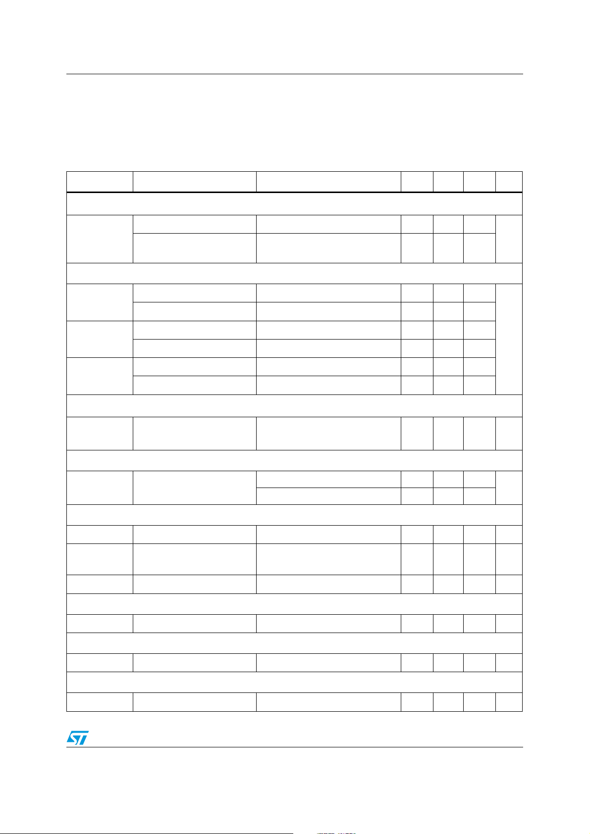
Table 5. Electrical characteristics
Symbol Parameter Test condition Min. Typ. Max. Unit
V
supply current
CC
VCC stand by current
I
CC
V
CC
Power-ON
Tu r n -O N V
5V BUS
Tu r n -O F F V
Tu r n -O N V
12V BUS
Tu r n -O F F V
Tu r n -O N V
V
V
CCDR
IN OK
regulation
Tu r n -O F F V
V
CCDR
Soft start and inhibit
I
SS
Soft start current
quiescent current
threshold V
CC
threshold V
CC
threshold V
CC
threshold V
CC
threshold
OCH
threshold
OCH
voltage
OSC = open; SS to GND 7 9
OSC= open;
HG = open, LG = open, PH=open
= 1.7V
OCH
= 1.7V
OCH
= 1.7V
OCH
= 1.7V
OCH
4.0 4.2 4.4
3.6 3.8 4.0
8.3 8.6 8.9
7.4 7.7 8.0
8.5 10
1.1 1.25 1.47
0.9 1.05 1.27
=5.5V to 14V
V
CC
= 1mA to 100mA
I
DR
4.5 5 5.5 V
SS = 2V 7 10 13
SS = 0 to 0.5V 20 30 45
mA
V
µA
Oscillator
f
OSC
f
OSC,RT
ΔV
OSC
Initial accuracy OSC = OPEN 380 400 420 kHz
Total accuracy
Ramp amplitude 2.1 V
Output voltage (1.2V MODE)
V
FB
Output voltage 1.190 1.2 1.208 V
Output voltage (0.6 MODE)
V
FB
Output voltage 0.597 0.6 0.603 V
Error amplifier
R
EAREF
EAREF input resistance Vs. GND 70 100 150 kΩ
RT = 390KΩ to V
RT = 18KΩ to GND
CCDR
-15 15 %
Doc ID 11938 Rev 3 11/52
Page 12
Electrical characteristics L6730 - L6730B
Table 5. Electrical characteristics (continued)
Symbol Parameter Test condition Min. Typ. Max. Unit
I
FB
I.I. bias current
= 0V
V
FB
0.290 0.5 μA
Ext Ref Clamp 2.3 V
V
OFFSET
G
V
Error amplifier offset Vref = 0.6V -5 +5 mV
Open loop voltage gain Guaranteed by design 100 dB
GBWP Gain-bandwidth product Guaranteed by design 10 MHz
SR Slew-rate
COMP = 10pF
Guaranteed by design
5V/μs
Gate drivers
R
HGATE_ON
R
HGATE_OFF
R
LGATE_ON
R
LGATE_OFF
High side source resistance
High side sink resistance
Low side source resistance
Low side sink resistance
V
BOOT
V
BOOT
V
CCDR
V
CCDR
- V
- V
= 5V
= 5V
PHASE
PHASE
= 5V
= 5V
1.7 Ω
1.12 Ω
1.15 Ω
0.6 Ω
Protections
I
OCH
I
OCL
OVP
I
OSC
OCH current source
OCL current source 90 100 110 μA
Over voltage trip
(V
FB
/ V
EAREF
)
OSC sourcing current
= 1.7V
V
OCH
V
rising
FB
V
V
V
V
= 0.6V
EAREF
falling
FB
= 0.6V
EAREF
> OVP Trip V
FB
OSC
= 3V
90 100 110 μA
120 %
117 %
30 mA
Power Good
V
PGOOD
Upper threshold
(V
FB
/ V
EAREF
)
Lower threshold
(VFB / V
EAREF
)
PGOOD voltage low
V
rising
FB
V
falling
FB
I
PGOOD
= -5mA
12/52 Doc ID 11938 Rev 3
108 110 112 %
88 90 92 %
0.5 V
Page 13
L6730 - L6730B Electrical characteristics
Table 6. Thermal characterizations (V
CC
= 12 V)
Symbol Parameter Test condition Min Typ Max Unit
Oscillator
f
OSC
Initial accuracy
OSC = OPEN;
= 0°C~ 125°C
T
J
376 400 424 kHz
Output voltage (1.2V MODE)
T
= 0°C~ 125°C
V
FB
Output voltage
J
= -40°C~ 125°C
T
J
1.188 1.2 1.212 V
1.185 1.2 1.212 V
Output voltage (0.6V MODE)
T
= 0°C~ 125°C
V
FB
Output voltage
J
T
= -40°C~ 125°C
J
0.596 0.6 0.605 V
0.593 0.6 0.605 V
Doc ID 11938 Rev 3 13/52
Page 14
Device description L6730 - L6730B
5 Device description
5.1 Oscillator
The switching frequency is internally fixed to 400 kHz. The internal oscillator generates the
triangular waveform for the PWM charging and discharging an internal capacitor (F
kHz). This current can be varied using an external resistor (R
and GND or V
in order to change the switching frequency. Since the OSC pin is
CCDR
) connected between OSC pin
T
maintained at fixed voltage (typ. 1.2 V), the frequency is increased (or decreased)
proportionally to the current sunk (sourced) from (into) the pin. In particular by connecting
R
versus GND the frequency is increased (current is sunk from the pin), according to the
T
following relationship:
6
1088.9
400
+=KRKHzFsw
⋅
OSC
Ω
(1)
)(
SW
= 400
Connecting R
to V
T
reduces the frequency (current is sourced into the pin), according
CCDR
to the following relationship:
7
1001.3
400
Switching frequency variation vs. R
Figure 4. Switching frequency variation versus RT
1500
1400
1300
1200
1100
1000
900
800
700
Fsw (KHz)
600
500
400
300
200
100
Rosc connected to GND
0 100 200 300 400 500 600 700 800 900 1000
is shown in Figure 4.
T
⋅
−=KRKHzFsw
OSC
)(
Ω
Rosc connected to Vccdr
Rosc (KOHM)
(2)
14/52 Doc ID 11938 Rev 3
Page 15
L6730 - L6730B Device description
5.2 Internal LDO
An internal LDO supplies the internal circuitry of the device. The input of this stage is the
V
pin and the output (5 V) is the V
CC
Figure 5. LDO block diagram
pin (see Figure 5).
CCDR
4.5V÷14V
LDO
5.3 Bypassing the LDO to avoid the voltage drop with low Vcc
The LDO can be by passed by providing 5 V voltage directly to V
V
pins must be shorted together as shown in Figure 6. V
CCDR
CCDR
at least 1 μF capacitor to sustain the internal LDO during the recharge of the bootstrap
capacitor. V
also represents a voltage reference for Tmask pin, S/O/U pin (L6730) or
CCDR
CC/O/U pin (L6730B) and PGOOD pin (see Table 4: Pin connection).
If Vcc
≈ 5 V the internal LDO works in dropout with an output resistance of about 1 Ω.
The maximum LDO output current is about 100 mA, and so the output voltage drop can be
100 mV. The LDO can be bypassed to avoid this.
. In this case Vcc and
CCDR
pin must be filtered with
Doc ID 11938 Rev 3 15/52
Page 16

Device description L6730 - L6730B
Figure 6. Bypassing the LDO
5.4 Internal and external references
It is possible to set two internal references, 0.6 V and 1.2 V, or provide an external reference
from 0 V to 2.5 V. The maximum value of the external reference depends on the V
V
= 4 V the clamp operates at about 2 V (typ.), while with VCC greater than 5 V the
CC
CC
: with
maximum external reference is 2.5 V (typ).
● V
● V
● V
from 0% to 80% of V
EAREF
from 80% to 95% of V
EAREF
from 95% to 100% of V
EAREF
−> External reference
CCDR
−> V
CCDR
CCDR
−> V
REF
REF
= 1.2 V
= 0.6 V
Providing an external reference from 0V to 450 mV the output voltage will be regulated but
some restrictions must be considered:
● The minimum OVP threshold is set at 300 mV.
● The under-voltage-protection doesn’t work.
● The PGOOD signal remains low.
To set the resistor divider it must be considered that a 100 kΩ pull-down resistor is
integrated into the device (see Figure 7.). Finally it must be taken into account that the
voltage at the EAREF pin is captured by the device at the start-up when Vcc is about 4 V.
16/52 Doc ID 11938 Rev 3
Page 17

L6730 - L6730B Device description
V
V
CC
V
V
V
V
V
5.5 Error amplifier
Figure 7. Error amplifier reference
DR
0.6
5.6 Soft-start
When both VCC and VIN are above their turn-on thresholds (VIN is monitored by the OCH
pin) the start-up phase takes place. Otherwise the SS pin is internally shorted to GND. At
start-up, a ramp is generated charging the external capacitor C
generator. The initial value for this current is 35 µA and charges the capacitor up to 0.5 V.
After that it becomes 10 µA until the final charge value of approximately 4 V (see Figure 5).
Figure 8. Device start-up: voltage at the SS pin
EAREF
100K
1.2
EXT
2.5
Error Amplifier Ref.
with an internal current
SS
cc
Vcc
in
Vin
4.2V
4.2V or 8.6V
1.25V
1.25V
t
Vss
ss
0.5V
0.5V
0.5V
4V
4V
t
Doc ID 11938 Rev 3 17/52
Page 18

Device description L6730 - L6730B
The output of the error amplifier is clamped with this voltage (Vss) until it reaches the
programmed value. No switching activity is observable if V
is lower than 0.5 V and both
SS
MOSFETs are off. When Vss is between 0.5 V and 1.1 V the low-side MOSFET is turned on
because the output of the error amplifier is lower than the valley of the triangular wave and
so the duty-cycle is 0%. As V
reaches 1.1 V (i.e. the oscillator triangular wave inferior
SS
limit) even the high-side MOSFET begins to switch and the output voltage starts to increase.
The L6730 - L6730B can only source current during the soft-start phase in order to manage
the pre-bias start-up applications. This means that when the startup occurs with output
voltage greater than 0V (pre-bias startup), even when Vss is between 0.5 V and 1.1 V the
low-side MOSFET is kept OFF (see Figure 9 and Figure 10).
Figure 9. Start-up without pre-bias
LGate
V
OUT
I
L
V
SS
Figure 10. Start-up with pre-bias
LGate
V
OUT
I
L
V
SS
The L6730B can always sink current and so it can be used to supply the DDR memory
termination BUS. If overcurrent is detected during the soft-start phase, the device provides
constant current-protection. In case there is short soft-start time and/or small inductor value
and/or high output capacitors value and thus, in case of high ripple current during the softstart, the converter can start-up in anyway and limit the current (Chapter 5.8: Monitoring and
18/52 Doc ID 11938 Rev 3
Page 19

L6730 - L6730B Device description
protection on page 21) but not enter into HICCUP mode. The soft-start phase ends when
V
reaches 3.5 V. After that the over current-protection triggers the HICCUP mode
SS
(L6730). With the L6730B there is the possibility to set the HICCUP mode or the constant
current mode after the soft-start acting on the multifunction pin CC/O/U. With the L6730 the
low-side MOSFET(s) management after soft-start phase depends on the S/O/U pin state
(see related section). If the sink mode is enabled the converter can sink current after softstart (see Figure 11) while, if the sink mode is disabled the converter never sinks current
(see Figure 12).
Figure 11. Sink mode enabled: Inductor current during and after soft-start (L6730)
V
OUT
V
SS
V
CC
I
L
During normal operation, if any under voltage is detected on one of the two supplies (V
V
), the SS pin is internally shorted to GND by an internal switch so the SS capacitor is
IN
CC
rapidly discharged. Two different turn-on UVLO thresholds can be set: 4.2 V for 5 V BUS
and 8.6 V for 12 V BUS.
Doc ID 11938 Rev 3 19/52
,
Page 20

Device description L6730 - L6730B
Figure 12. Sink mode disabled: Inductor current during and after soft-start (L6730)
Vout
Vss
Vcc
I
L
5.7 Driver section
The high-side and low-side drivers allow for the use of different types of power MOSFETs
(also multiple MOSFETs to reduce the R
low-side driver is supplied by V
A predictive dead time control avoids MOSFETs cross-conduction maintaining very short
dead time duration (see Figure 13.).
The control monitors the phase node in order to sense the low-side body diode recirculation.
If the phase node voltage is less than a certain threshold (–350 mV typ.) during the dead
time, it will be reduced in the next PWM cycle. The predictive dead time control does not
work when the high-side body diode is conducting because the phase node does not go
), maintaining fast switching transitions. The
DSON
while the high-side driver is supplied by the BOOT pin.
CCDR
20/52 Doc ID 11938 Rev 3
Page 21

L6730 - L6730B Device description
(
⋅
=
negative. This situation happens when the converter is sinking current for example and, in
this case, an adaptive dead time control operates.
Figure 13. Dead times
5.8 Monitoring and protection
The output voltage is monitored by the FB pin. If it is not within ±10% (typ.) of the
programmed value, the Power-Good (PGOOD) output is forced low. The PGOOD signal can
be delayed by adding an external capacitor on PGDelay pin (see Table 4: Pin connection
and Figure 14.); this can be useful to perform cascade sequencing. The delay can be
calculated with the following formula:
The device provides over voltage protection: when the voltage sensed on FB pin reaches a
value 20% (typ) greater than the reference, the low-side driver is turned on. If the OVP notlatched mode has been set the low-side MOSFET is kept on as long as the overvoltage is
detected (see Figure 15.).The OVP latched-mode has been set the low-side MOSFET is
)
pFCPGDelay
5.0
Doc ID 11938 Rev 3 21/52
Page 22

Device description L6730 - L6730B
turned on until VCC is toggled (see Figure 16). In case of latched-mode OVP the OSC pin is
forced high (4.5 V typ) if an over voltage is detected.
Figure 14. PGOOD signal
FB
PGOOD
2ms/Div.
Figure 15. OVP not latched
LGate
FB
OSC
22/52 Doc ID 11938 Rev 3
Page 23

L6730 - L6730B Device description
Figure 16. OVP latched
LGate
OSC
FB
There is an electrical network between the output terminal and the FB pin and therefore the
voltage at this pin is not a perfect replica of the output voltage. If the converter can sink
current, in the most of cases the low-side will be turned on before the output voltage
exceeds the over-voltage threshold because the error amplifier will throw off balance in
advance.
Even if the device does not report an overvoltage event, the behavior is the same because
the low-side is turned on immediately. Instead, if the sink mode is disabled, the low-side will
be turned on only when the overvoltage protection (OVP) operates and not before because
the current can not be reversed. In this case, a delay between the output voltage rising and
FB voltage rising can appear and the OVP can turn on late. Figure 17 and Figure 18 show
an overvoltage event in the cases of the sink being enabled or disabled. The output voltage
rises with a slope of 100 mVµs, emulating the breaking of the high-side MOSFET as an
overvoltage occurs.
Doc ID 11938 Rev 3 23/52
Page 24

Device description L6730 - L6730B
Figure 17. OVP with sink enabled: the low-side MOSFET is turned-on in advance
V
OUT
109%
FB
V
LGate
Figure 18. OVP with sink disabled: delay on the OVP operation
126%
V
OUT
V
FB
LGate
The L6730B can always sink current and so the OVP will operate always in advance. The
device realizes the over-current-protection (OCP) sensing the current both on the high-side
MOSFET(s) and the low-side MOSFET(s) and so 2 current limit thresholds can be set (see
OCH pin and OCL pin in Table 4: Pin connection):
● Peak current limit
● Valley current limit
The peak current protection is active when the high-side MOSFET(s) is turned on, after an
adjustable masking time (see Chapter 5.10 on page 27). The valley-current-protection is
enabled when the low-side MOSFET(s) is turned on after a fix masking time of about 400
ns. If, when the soft-start phase is completed, an over current event occurs during the on
time (peak-current-protection) or during the off time (valley-current-protection) the device
24/52 Doc ID 11938 Rev 3
Page 25

L6730 - L6730B Device description
−
enters in HICCUP mode (L6730): the high-side and low-side MOSFET(s) are turned off, the
soft-start capacitor is discharged with a constant current of 10 µA and when the voltage at
the SS pin reaches 0.5 V the soft-start phase restarts. During the soft-start phase the OCP
provides a constant-current-protection. If during the T
the OCH comparator triggers an
ON
over current the high-side MOSFET(s) is immediately turned-off (after the masking time and
the internal delay) and returned-on at the next pwm cycle. The limit of this protection is that
the Ton can’t be less than masking time plus propagation delay (see Chapter 5.9: Adjustable
masking time on page 27) because during the masking time the peak-current-protection is
disabled. In case of very hard short circuit, even with this short T
, the current could
ON
escalate. The valley-current-protection is very helpful in this case to limit the current. If
during the off-time the OCL comparator triggers an over current, the high-side MOSFET(s)
is not turned-on until the current is over the valley-current-limit. This implies that, if it is
necessary, some pulses of the high-side MOSFET(s) will be skipped, guaranteeing a
maximum current due to the following formula:
VoutVin
II
+=
T
⋅
L
(4)
MINONVALLEYMAX
,
In constant current protection a current control loop limits the value of the error amplifier’s
output (comp), in order to avoid its saturation and thus recover faster when the output
returns in regulation. Figure 19 shows the behaviour of the device during an over current
condition that persists also in the soft-start phase.
Figure 19. Constant current and hiccup mode during an OCP (L6730)
VSS
VCOMP
I
L
Using the L6730B there is the possibility to set the constant-current-protection also after the
soft-start. The following figures show the behaviour of the L6730B during an overcurrent
event.
Figure 20 shows the intervention of the peak OCP: the high-side MOSFET(s) is turned-off
when the current exceeds the OCP threshold. In this way the duty-cycle is reduced, the
V
is reduced and so the maximum current can be fixed even if the output current is
OUT
escalating. Figure 21 shows the limit of this protection: the on-time can be reduced only to
the masking time and, if the output current continues to increase, the maximum current can
increase too. Notice how the Vout remains constant even if the output current increases
because the on-time cannot be reduced anymore.
Doc ID 11938 Rev 3 25/52
Page 26

Device description L6730 - L6730B
Figure 20. Peak overcurrent-protection in constant-current-protection (L6730B)
V
OUT
Peak th
T
I
L
Figure 21. Peak OCP in case of heavy overcurrent (L6730B)
I
OUT
ON
V
OUT
I
L
I
OUT
If the current is higher than the valley OCP threshold during the off-time, the high-side
MOSFET(s) will not be turned ON. In this way the maximum current can be limited
(Figure 22).
During the constant-current-protection if the Vout becomes lower than 80% of the
programmed value an UV (under-voltage) is detected and the device enters in HICCUP
mode. The under-voltage-lock-out (UVLO) is adjustable by the multifunction pin (see
Chapter 5.10 on page 27). It’s possible to set two different thresholds:
● 4.2 V for 5 V bus
● 8.6 V for 12 V bus
26/52 Doc ID 11938 Rev 3
Page 27

L6730 - L6730B Device description
Working with a 12 V BUS, setting the UVLO at 8.6 V can be very helpful to limit the input
current in case of BUS fall.
Figure 22. Valley OCP (L6730B)
V
OUT
Valley th
I
L
T
OFF
T
OFF
5.9 Adjustable masking time
By connecting the masking time pin to V
values for the peak current protection leading edge blanking time. This is useful to avoid any
false OCP trigger due to spikes and oscillations generated at the turn-on of the high-side
MOSFET(s). The amount of this noise depends very much on the layout, MOSFETs, freewheeling diode, switched current, and input voltage.
When good layout and medium current are used, the minimum masking time can be
chosen, while in case of higher noise, it is better to select the maximum masking time. By
connecting the t
MASK
pin to V
the masking time is about 400 ns, while connecting it to
CCDR
GND results in about 260 ns masking time.
or GND it is possible to select two different
CCDR
5.10 Multifunction pin (S/O/U L6730) (CC/O/U L6730B)
With this pin it is possible:
● To enable disable the sink mode current capability (L6730) or the constant current
protection (L6730B) at the end of the soft-start
● To enable or disable the latch-mode for the OVP
● To set the UVLO threshold for 5 V BUS and 12 V busses
Doc ID 11938 Rev 3 27/52
Page 28

Device description L6730 - L6730B
⋅≤≤
Ta bl e 7 shows how to set the different options through an external resistor divider:
Figure 23. External resistor
R1
R2
VCCDR
S/O/U
CC/O/U
L6730/B
Table 7. S/O/U and CC/O/U pin
R1 R2
N.C 0Ω 0 5V BUS Not latched Not
11KΩ 2.7KΩ 0.2 5V BUS Not latched Yes
6.2KΩ 2.7KΩ 0.3 5V BUS Latched Not
4.3KΩ 2.7KΩ 0.4 5V BUS Latched Yes
2.7KΩ 2.7KΩ 0.5 12V BUS Not latched Not
1.8KΩ 2.7KΩ 0.6 12V BUS Not latched Yes
1.2KΩ 2.7KΩ 0.7 12V BUS Latched Not
0Ω N.C 1 12V BUS Latched Yes
5.11 Synchronization
The presence of many converters on the same board can generate beating frequency noise.
To avoid this it is important to make them operate at the same switching frequency.
Moreover, a phase shift between different modules helps to minimize the RMS current on
the common input capacitors. Figure 24 shows the results of two modules in
synchronization. Two or more devices can be synchronized simply connecting together the
SYNCH pins. The device with the higher switching frequency will be the Master while the
other one will be the slave. The slave controller will increase its switching frequency
reducing the ramp amplitude proportionally and then the modulator gain will be increased.
V
SOU/VCCDR
UVLO OVP SINK CC
To avoid a huge variation of the modulator gain, the best way to synchronize two or more
devices is to make them work at the same switching frequency and, in any case, the
switching frequencies can differ for a maximum of 50% of the lowest one. If, during
synchronization between two (or more) L6730, it’s important to know in advance which the
master is, it’s timely to set its switching frequency at least 15% higher than the slave. Using
an external clock signal (f
different switching frequency (f
28/52 Doc ID 11938 Rev 3
) to synchronize one or more devices that are working at a
EXT
) it is recommended to follow the below formula:
SW
fff
3,1
SWEXTSW
Page 29

L6730 - L6730B Device description
The phase shift between master and slaves is approximately done 180°.
Figure 24. Synchronization
PWM SIGNALS
INDUCTOR CURRENTS
5.12 Thermal shutdown
When the junction temperature reaches 150°C ±10°C, the device enters in thermal
shutdown.
Both MOSFETs are turned OFF and the soft-start capacitor is rapidly discharged with an
internal switch. The device does not restart until the junction temperature goes down to
120°C and, in any case, until the voltage at the soft-start pin reaches 500 mV.
5.13 Minimum ON-time T
The device can manage minimum ON times lower than 100 ns. This feature comes from the
control topology as well as from the particular L6730/B overcurrent protection system. In a
voltage mode controller, the current does not have to be sensed to perform regulation and,
in the case of L6730/B, it does not have to be sensed for the overcurrent protection either
because valley current protection can operate during the OFF time. The first advantage
related of this feature is the achievement of extremely low conversion ratios. Figure 25
shows a conversion from 14 V to 0.5 V at 820 kHz with a t
limited by the MOSFET turn-on and turn-off times.
ON(MIN)
ON of about 50 ns. The ON time is
Doc ID 11938 Rev 3 29/52
Page 30

Device description L6730 - L6730B
Figure 25. 14 V -> 0.5 V@820 kHz, 5 A
50ns
5.14 Bootstrap anti-discharging system
This built-in anti-discharging system keeps the voltage going across the bootstrap capacitor
from going below 3.3 V. An internal comparator senses the voltage across the external
bootstrap capacitor and helps to keep it charged, eventually turning on the low-side
MOSFET for approximately 200 ns. If the bootstrap capacitor is not charged up enough, the
high-side MOSFET cannot be effectively turned on and it will present a higher R
some cases, the OCP can be also triggered. There are up to two conditions during which
the bootstrap capacitor can be discharged:
● fan power supply failure, and
● no sink at zero current operation.
DS(on)
. In
30/52 Doc ID 11938 Rev 3
Page 31

L6730 - L6730B Device description
5.14.1 Fan power supply failure
In many applications the fan is driven by a DC motor that uses a DC/DC converter. Often
only the speed of the motor is controlled by varying the voltage applied to the input terminal
and there is no control on the torque because the current is not directly controlled. The
current has to be limited in case of overload or short-circuit, but without stopping the motor.
With the L6730B, the current can be limited without shutting down the system because
constant current protection is provided. In order to vary the motor speed, the output voltage
of the converter must be varied. Both L6730 and L6730B have a dedicated EAREF pin (see
Figure 4) which provides an external reference to the non-inverting input of the error-
amplifier.
In these applications the duty cycle depends on the motor’s speed and sometimes a 100%
duty cycle setting has to be used to attain the maximum speed. In these conditions, the
bootstrap capacitor can not be recharged and the system cannot work properly. Some PWM
controllers limit the maximum duty cycle to 80 or 90% in order to keep the bootstrap
capacitor charged, but this makes performance during the load transient worse. The
“bootstrap anti-discharging system” allows the L6730x to work at 100% without any
problem.
Figure 26.: 100% duty cycle operation on page 31 shows the following picture illustrates the
device behavior when the input voltage is 5 V and a 100% duty cycle is set by an external
reference.
Figure 26. 100% duty cycle operation
TOFF≈200ns
5.14.2 No-sink at zero current operation
The L6730 can work in no-sink mode. If output current is zero the converter skip some
pulses and works with a lower switching frequency. Between two pulses can pass a
relatively long time (say 200-300 µs) during which there’s no switching activity and the
current into the inductor is zero. In this condition the phase node is at the output voltage and
in some cases this is not enough to keep the bootstrap cap charged. For example, if Vout is
3.3 V the voltage across the bootstrap cap is only 1.7 V. The high-side MOSFET cannot be
Vout=5V
Vin=5V
LGate
≈
Fsw?6.3KHz
Doc ID 11938 Rev 3 31/52
Page 32

Device description L6730 - L6730B
effectively turned-on and the regulation can be lost. Thanks to the “bootstrap antidischarging system” the bootstrap cap is always kept charged. The following picture shows
the behaviour of the device in the following conditions: 12 V -> 3.3 V@0 A.
It can be observed that between two pulses trains the low-side is turned-on in order to keep
the bootstrap cap charged.
Figure 27. 12 V -> 3.3 V@0 A in no-sink
I
L
V
BOOT
Pulse trainMinimum Bootstrap Voltage V
PHASE
32/52 Doc ID 11938 Rev 3
Page 33

L6730 - L6730B Application details
−
V
H
V
V
V
6 Application details
6.1 Inductor design
The inductance value is defined by a compromise between the transient response time, the
efficiency, the cost and the size. The inductor has to be calculated to maintain the ripple
current (ΔI
can be calculated with the following relationship:
) between 20% and 30% of the maximum output current. The inductance value
L
Vout
VoutVin
≅
L
⋅
Δ⋅
IFsw
L
(6)
Vin
Where F
is the switching frequency, VIN is the input voltage and V
SW
is the output
OUT
voltage. Figure 28 shows the ripple current vs. the output voltage for different values of the
inductor, with V
= 5 V and VIN = 12 V at a switching frequency of 400 kHz.
IN
Increasing the value of the inductance reduces the current ripple but, at the same time,
increases the converter response time to a load transient. If the compensation network is
well designed, during a load transient the device is able to set the duty cycle to 100% or to
0%. When one of these conditions is reached, the response time is limited by the time
required to change the inductor current. During this time the output current is supplied by
the output capacitors. Minimizing the response time can minimize the output capacitor size.
Figure 28. Inductor current ripple
8
7
6
5
4
3
2
1
INDUCTOR CURRENT RIPPL
0
01234
OUTPUT VOLTAGE (V)
in=12V, L=1uH
in=12V, L=2uH
in=5V, L=500n
in=5V, L=1.5uH
Doc ID 11938 Rev 3 33/52
Page 34

Application details L6730 - L6730B
⋅Δ=
Δ
6.2 Output capacitors
The output capacitors are basic components for the fast transient response of the power
supply. They depend on the output voltage ripple requirements, as well as any output
voltage deviation requirement during a load transient. During a load transient, the output
capacitors supply the current to the load or absorb the current stored into the inductor until
the converter reacts. In fact, even if the controller recognizes immediately the load transient
and sets the duty cycle at 100% or 0%, the current slope is limited by the inductor value. The
output voltage has a first drop due to the current variation inside the capacitor (neglecting
the effect of the ESL):
(7)
ESR
Moreover, there is an additional drop due to the effective capacitor discharge or charge that
is given by the following formulas:
Vout
COUT
=Δ
Vout
COUT
=Δ
2
ESRIoutVout
2
LIout
⋅Δ
VoutDVinCout
−⋅⋅⋅
2
LIout
⋅Δ
VoutCout
⋅⋅
(9)
(8)
)maxmin,(2
Formula (8) is valid in case of positive load transient while the formula (9) is valid in case of
negative load transient. D
For a given inductor value, minimum input voltage, output voltage and maximum load
transient, a maximum ESR, and a minimum C
values also affect the static output voltage ripple. In the worst case the output voltage ripple
can be calculated with the following formula:
Usually the voltage drop due to the ESR is the biggest one while the drop due to the
capacitor discharge is almost negligible.
6.3 Input capacitors
The input capacitors have to sustain the RMS current flowing through them, that is:
Where D is the duty cycle. The equation reaches its maximum value, I
The losses in worst case are:
is the maximum duty cycle value that in the L6730/B is 100%.
MAX
value can be set. The ESR and C
OUT
+⋅Δ=Δ
(
ESRIVout
L
1
8
)
(12)
(10)
/2 with D = 0.5.
OUT
⋅⋅
FswCout
(11)
)1( DDIoutIrms −⋅⋅=
2
)5.0( IoutESRP ⋅⋅=
OUT
34/52 Doc ID 11938 Rev 3
Page 35

L6730 - L6730B Application details
6.4 Compensation network
The loop is based on a voltage mode control (Figure 29). The output voltage is regulated to
the internal/external reference voltage and scaled by the external resistor divider. The error
amplifier output V
pulse-width modulated (PWM) with an amplitude of V
is filtered by the output filter. The modulator transfer function is the small signal transfer
function of V
OUT/VCOMP
L-Cout resonance and a zero at F
Gain of the modulator is simply the input voltage V
voltage: V
OSC
.
Figure 29. Compensation network
is then compared with the oscillator triangular wave to provide a
COMP
at the PHASE node. This waveform
IN
. This function has a double pole at frequency FLC depending on the
depending on the output capacitor’s ESR. The DC
ESR
divided by the peak-to-peak oscillator
IN
Z
FB
Z
IN
The compensation network consists in the internal error amplifier, the impedance networks
Z
(R3, R4 and C20) and Z
IN
(R5, C18 and C19). The compensation network has to
FB
provide a closed loop transfer function with the highest 0dB crossing frequency to have
fastest transient response (but always lower than fsw/10) and the highest gain in DC
conditions to minimize the load regulation error. A stable control loop has a gain crossing the
Doc ID 11938 Rev 3 35/52
Page 36

Application details L6730 - L6730B
0 dB axis with -20 dB/decade slope and a phase margin greater than 45°. To locate poles
and zeroes of the compensation networks, the following suggestions may be used:
● Modulator singularity frequencies:
ω
● Compensation network singularity frequencies:
=
ω
P
1
ω
Z
● Compensation network design:
– Put the gain R
–Place
–Place
–Place
–Place
ω
before the output filter resonance ωLC;
Z1
ω
at the output filter resonance ωLC;
Z2
ω
at the output capacitor ESR zero ω
P1
ω
at one half of the switching frequency;
P2
1
=
CoutLLC⋅
1
⎛
⎜
⋅
R
5
⎜
⎝
1
=
1
⋅
CR
in order to obtain the desired converter bandwidth
5/R3
(13)
⎞
⋅
CC
1918
⎟
⎟
+
CC
1918
⎠
(17)
195
R
5
⋅=
R
3
(15)
Vin
Δ
Vosc
ω
ESR
ω
P
2
=
ω
2
Z
ϖϖ
⋅
LCC
1
=
=
CoutESR
⋅
1
⋅
(16)
CR
204
1
()
+⋅
RRC
4320
(18)
;
ESR
– Check the loop gain considering the error amplifier open loop gain.
(14)
(18)
Figure 30. Asymptotic bode plot of converter's open loop gain
36/52 Doc ID 11938 Rev 3
Page 37

L6730 - L6730B Application details
6.5 Two quadrant or one quadrant operation mode (L6730)
After the soft-start phase the L6730 can work in source only (one quadrant operation mode)
or in sink/source (two quadrant operation mode), depending on the setting of the
multifunction pin (see Chapter 5.10 on page 27). The choice of one or two quadrant
operation mode is related to the application. One quadrant operation mode permits to have
a higher efficiency at light load, because the converter works in discontinuous mode (see
Figure 31). Nevertheless in some cases, in order to maintain a constant switching
frequency, it’s preferable to work in two quadrants, even at light load. In this way the
reduction of the switching frequency due to the pulse skipping is avoided. To parallel two or
more modules is requested the one quadrant operation in order not to have current sinking
between different converters. Finally the two quadrant operation allows faster recovers after
negative load transient. For example, let’s consider that the load current falls down from I
to 0A with a slew rate sufficiently greater than L/V
(where L is the inductor value). Even
OUT
considering that the converter reacts instantaneously setting to 0% the duty-cycle, the
energy ½*L*I
2
stored in the inductor will be transferred to the output capacitors,
OUT
increasing the output voltage. If the converter can sink current this overvoltage can be faster
eliminated.
Figure 31. Efficiency in discontinuous-current-mode and continuous-current-mode
EFFICIENCY: DCM vs. CCM
OUT
0.7
0.6
0.5
0.4
EFF. (%
0.3
0.2
0.1
0 0.2 0.4 0.6 0.8 1 1.2 1.4 1.6 1.8 2
OUTPUT CURRENT (A)
EFFICIENCY DCM
EFFICIENCY CCM
Doc ID 11938 Rev 3 37/52
Page 38

L6730 demonstration board L6730 - L6730B
7 L6730 demonstration board
7.1 Description
L6730 demonstration board realizes in a four layer PCB a step-down DC/DC converter and
shows the operation of the device in a general purpose application. The input voltage can
range from 4.5 V to 14 V and the output voltage is at 3.3 V. The module can deliver an
output current in excess of 30 A. The switching frequency is set at 400 kHz (controller freerunning F
the UVLO threshold (5 V or 12 V bus), the OVP intervention mode and the sink-mode
current capability.
Figure 32. Demonstration board picture
) but it can be increased up to 1 MHz. A 7 positions dip-switch allows to select
SW
Top Side Bottom Side
38/52 Doc ID 11938 Rev 3
Page 39

L6730 - L6730B L6730 demonstration board
7.2 PCB layout
Figure 33. Top layer Figure 34. Power ground layer
Figure 35. Signal ground layer Figure 36. Bottom layer
Doc ID 11938 Rev 3 39/52
Page 40

L6730 demonstration board L6730 - L6730B
Figure 37. Demonstration board schematic
Table 8. Demonstration board part list
Reference Value Manufacturer Package Supplier
R1 820Ω Neohm SMD 0603 IFARCAD
R2 0Ω Neohm SMD 0603 IFARCAD
R3 N.C.
R4
R5
R6
R7
R8
R9
R10
R11
R12
R13
10Ω 1% 100mW
11K 1% 100mW
6K2 1% 100mW
4K3 1% 100mW
2K7 1% 100mW
1K8 1% 100mW
1K2 1% 100mW
2K7 1% 100mW
1K
2K7 1% 100mW
40/52 Doc ID 11938 Rev 3
Neohm SMD 0603 IFARCAD
Neohm SMD 0603 IFARCAD
Neohm SMD 0603 IFARCAD
Neohm SMD 0603 IFARCAD
Neohm SMD 0603 IFARCAD
Neohm SMD 0603 IFARCAD
Neohm SMD 0603 IFARCAD
Neohm SMD 0603 IFARCAD
Neohm SMD 0603 IFARCAD
Neohm SMD 0603 IFARCAD
Page 41

L6730 - L6730B L6730 demonstration board
Table 8. Demonstration board part list (continued)
Reference Value Manufacturer Package Supplier
R14
R15
R16
R17
R18
R19
R20
R21
R22
R23
C1
C3-C7-C9-C15-C21
C2
C4-C6
C8
C10
C11
C12
C13
C14
C18-C19
C20
L1
D1
D2
Q1-Q2
Q4-Q5
U1
1K 1% 100mW
1K 1% 100mW
4K7 1% 100mW
N.C.
2.2Ω
2.2Ω
10K 1% 100mW
N.C.
N.C.
0Ω
220nF
100nF
1nF.
100uF 20V
4.7uF 20V
10nF
N.C.
47nF
1.5nF
4.7nF
330uF 6.3V
N.C.
1.8uH
1N4148
STS1L30M
STS12NH3LL
STSJ100NH3LL
L6730
Neohm SMD 0603 IFARCAD
Neohm SMD 0603 IFARCAD
Neohm SMD 0603 IFARCAD
Neohm SMD 0603 IFARCAD
Neohm SMD 0603 IFARCAD
Neohm SMD 0603 IFARCAD
Neohm SMD 0603 IFARCAD
Kemet SMD 0603 IFARCAD
Kemet SMD 0603 IFARCAD
Kemet SMD 0603 IFARCAD
OSCON 20SA100M RADIAL 10X10.5 SANYO
AVX SMA6032 IFARCAD
Kemet SMD 0603 IFARCAD
Kemet SMD 0603 IFARCAD
Kemet SMD 0603 IFARCAD
Kemet SMD 0603 IFARCAD
POSCAP 6TPB330M SMD SANYO
Panasonic SMD ST
ST SOT23 IFARCAD
ST DO216AA ST
ST SO8 ST
ST SO8 ST
ST HTSSOP20 ST
SWITCH DIP SWITCH 7 POS. ST
Doc ID 11938 Rev 3 41/52
Page 42

L6730 demonstration board L6730 - L6730B
Table 9. Other inductor manufacturer
Manufacturer Series Inductor value (µH) Saturation current (A)
WURTH ELEKTRONIC 744318180 1.8 20
SUMIDA CDEP134-2R7MC-H 2.7 15
EPCOS HPI_13 T640 1.4 22
TDK SPM12550T-1R0M220 1 22
TOKO FDA1254 2.2 14
COILTRONICS
HCF1305-1R0 1.15 22
HC5-1R0 1.3 27
Table 10. Other capacitor manufacturer
Manufacturer Series Capacitor value (µF) Rated voltage (V)
TDK
NIPPON CHEMI-CON 25PS100MJ12 100 25
PANASONIC ECJ4YB0J107M 100 6.3
C4532X5R1E156M 15 25
C3225X5R0J107M 100 6.3
42/52 Doc ID 11938 Rev 3
Page 43

L6730 - L6730B I/O Description
8 I/O Description
Figure 38. Demonstration board
Table 11. I/O functions
Symbol Function
The input voltage can range from 1.8V to 14V. If the input voltage is between
Input (Vin-Gin)
Output (V
V
CC
OUT-GOUT
-GND
V
CCDR
TP1
CC
4.5V and 14V it can supply also the device (through the V
case the pin 1 and 2 of the jumper G1 must be connected together.
The output voltage is fixed at 3.3V but it can be changed by replacing the
resistor R14 of the output resistor divider:
)
The over-current-protection limit is set at 15A but it can be changed by
replacing the resistors R1 and R12 (see OCL and OCH pin in Ta bl e 4 : P in
connection).
Using the input voltage to supply the controller no power is required at this
input. However the controller can be supplied separately from the power stage
through the V
input (4.5-14V) and, in this case, jumper G1 must be left
CC
open.
An internal LDO provides the power into the device. The input of this stage is
the VCC pin and the output (5V) is the V
providing directly a 5V voltage from V
and 3 of the jumper G1 must be shorted.
This pin can be used as an input or as a test point. If all the jumper G2 pins are
shorted, TP1 can be used as a test point of the voltage at the EAREF pin. If
the pins 2 and 3 of G2 are connected together, TP1 can be used as an input to
provide an external reference for the internal error amplifier (see section 4.3.
Internal and external references).
pin) and in this
CC
R
VVo
REF
16
)1(
+⋅=
R
14
pin. The LDO can be bypassed,
CCDR
and Gndcc. In this case the pins 1
CCDR
Doc ID 11938 Rev 3 43/52
Page 44

I/O Description L6730 - L6730B
Table 11. I/O functions (continued)
Symbol Function
TP2 This test point is connected to the Tmask pin (see Table 4: Pin connection).
TP3 This test point is connected to the S/O/U pin (see Chapter 5.10 on page 27).
SYNCH
PWRGD This pin is connected to the PGOOD pin of the controller.
DIP SWITCH
This pin is connected to the synch pin of the controller (see Chapter 5.11 on
page 28).
Different positions of the dip switch correspond to different settings of the
multifunction pin (S/O/U) (CC/O/U).
Table 12. Dip switch
UVLO OVP SINK CC
5V Not latched Not 0 S7 A
5V Not latched Yes 0.2 S1-S7 B
5V Latched Not 0.3 S2-S7 C
5V Latched Yes 0.4 S3-S7 D
12V Not latched Not 0.5 S4-S7 E
12V Not latched Yes 0.6 S5-S7 F
12V Latched Not 0.7 S6-S7 G
12V Latched Yes 1 S1 H
Vsou/V
CCDR
DIP switch State
44/52 Doc ID 11938 Rev 3
Page 45

L6730 - L6730B Efficiency
Y
Y
9 Efficiency
The following figures show the demo board efficiency versus load current for different values
of input voltage and switching frequency:
Figure 39. Demonstration board efficiency 400 kHz
Fsw=400KHz
95.00%
VO = 3.3V
90.00%
85.00%
EFFICIENC
80.00%
75.00%
V
VIN = 5V
IN = 5VVIN = 5V
VIN = 12V
13579111315
Iout (A)
Figure 40. Demonstration board efficiency 645 kHz
Fsw=645KHz
95.00%
90.00%
85.00%
80.00%
EFFICIENC
75.00%
VIN = 5V
VIN = 12V
V
O
= 3.3V
70.00%
13579111315
Iout (A)
Doc ID 11938 Rev 3 45/52
Page 46

Efficiency L6730 - L6730B
Y
Figure 41. Demonstration board efficiency 1 MHz
Fsw=1MHz
VO = 3.3V
95.00%
90.00%
85.00%
VIN = 5V
80.00%
75.00%
EFFICIENC
70.00%
65.00%
60.00%
13579111315
Iout (A)
Figure 42. Efficiency with 2xSTS12NH3LL+2XSTSJ100NH3LL
12V-->3.3V
0.96
0.95
0.94
0.93
0.92
0.91
0.9
EFFICIENCY (%)
0.89
0.88
0.87
3 5 7 9 11 13 15 17 19
VIN = 12V
400KHz
700KHz
1MHz
OUTPUT CURRENT (A)
46/52 Doc ID 11938 Rev 3
Page 47

L6730 - L6730B POL demonstration board
10 POL demonstration board
10.1 Description
A compact demonstration board has been designed to manage currents in the range of 1015 A. Figure 39 shows the schematic and Tab l e 10 the part list. Multi-layer-ceramiccapacitors (MLCCs) have been used on the input and the output in order to reduce the
overall size.
Figure 43. Pol demonstration board schematic
Table 13. Pol demonstration board part list
Reference Value Manufacturer Package Supplier
R1
R2
R3
R4
R5
R6
R7
R8
R9
R10
1K8Ω
10KΩ
N.C.
10Ω
11K 1% 100mW
2K7 1% 100mW
N.C.
0Ω
3K 1% 100mW
4K7 1% 100mW
Neohm SMD 0603 IFARCAD
Neohm SMD 0603 IFARCAD
Neohm SMD 0603 IFARCAD
Neohm SMD 0603 IFARCAD
Neohm SMD 0603 IFARCAD
Neohm SMD 0603 IFARCAD
Neohm SMD 0603 IFARCAD
Neohm SMD 0603 IFARCAD
Neohm SMD 0603 IFARCAD
Doc ID 11938 Rev 3 47/52
Page 48

POL demonstration board L6730 - L6730B
Y
Table 13. Pol demonstration board part list (continued)
Reference Value Manufacturer Package Supplier
R11
R12
R13
R14
R15
C1-C7
C6- C19-C20-C9
C2
C11
C12
C13
C8
C14
C3-C4-C5
C15-C16-C17-C18
L1
D1
Q1
Q2
U1
15Ω 1% 100mW
4K7 1% 100mW
1K 1% 100mW
2.2Ω
2.2Ω
220nF
100nF
1nF
N.C.
68nF
220pF
4.7uF 20V
6.8nF
15uF
100uF
1.8uH
STS1L30M
STS12NH3LL
STSJ100NH3LL
L6730
Neohm SMD 0603 IFARCAD
Neohm SMD 0603 IFARCAD
Neohm SMD 0603 IFARCAD
Neohm SMD 0603 IFARCAD
Neohm SMD 0603 IFARCAD
Kemet SMD 0603 IFARCAD
Kemet SMD 0603 IFARCAD
Kemet SMD 0603 IFARCAD
Kemet SMD 0603 IFARCAD
Kemet SMD0603 IFARCAD
AVX SMA6032 IFARCAD
Kemet SMD 0603 IFARCAD
TDK MLC
C4532X5R1E156M
PANASONIC MLC
P/N ECJ4YBOJ107M
SMD1812 IFARCAD
SMD 1210 IFARCAD
Panasonic SMD ST
ST DO216AA ST
ST POWER SO8 ST
ST POWER SO8 ST
ST HTSSOP20 ST
Figure 44. Pol demonstration board efficiency
12V-->3.3V@400KHz
0.94
0.92
0.9
0.88
0.86
EFFICIENC
0.84
0.82
1357911
OUTP UT CURRENT (A)
48/52 Doc ID 11938 Rev 3
Page 49

L6730 - L6730B Package mechanical data
11 Package mechanical data
In order to meet environmental requirements, ST offers these devices in different grades of
ECOPACK
®
packages, depending on their level of environmental compliance. ECOPACK®
specifications, grade definitions and product status are available at: www.st.com.
ECOPACK is an ST trademark.
Table 14. HTSSOP20 mechanical data
mm inch
Dim.
Min. Typ. Max. Min. Typ. Max.
A 1.200 0.047
A1 0.150 0.006
A2 0.800 1.000 1.050 0.031 0.039 0.041
b 0.190 0.300 0.007 0.012
c 0.090 0.200 0.003 0.008
(1)
D
(3)
D1
2.200 0.087
E 6.200 6.400 6.600 0.244 0.252 0.260
(2)
E1
(3)
E2
e 0.650 0.025
6.400 6.500 6.600 0.252 0.256 0.260
4.300 4.400 4.500 0.170 0.173 0.177
1.500 0.059
L 0.450 0.600 0.750 0.018 0.024 0.030
L1 1.000 0.039
k 0° min., 8° max.
aaa 0.100 0.004
1. Dimension “D” does not include mold flash, protrusions or gate burrs. Mold flash, protrusions or gate burrs
shall not exceed 0.15mm per side.
2. Dimension “E1” does not include interlead flash or protrusions. Intelead flash or protrusions shall not
exceed 0.25mm per side.
3. The size of exposed pad is variable depending of leadframe design pad size. End user should verify “D1”
and “E2” dimensions for each device application.
Doc ID 11938 Rev 3 49/52
Page 50

Package mechanical data L6730 - L6730B
Figure 45. Package dimensions
50/52 Doc ID 11938 Rev 3
Page 51

L6730 - L6730B Revision history
12 Revision history
Table 15. Document revision history
Date Revision Changes
21-Dec-2005 1 Initial release
29-May-2006 2 New template, thermal data updated
07-Dec-2009 3 Updated Table 4 on page 8 and added Section 1.2 on page 6
Doc ID 11938 Rev 3 51/52
Page 52

L6730 - L6730B
Please Read Carefully:
Information in this document is provided solely in connection with ST products. STMicroelectronics NV and its subsidiaries (“ST”) reserve the
right to make changes, corrections, modifications or improvements, to this document, and the products and services described herein at any
time, without notice.
All ST products are sold pursuant to ST’s terms and conditions of sale.
Purchasers are solely responsible for the choice, selection and use of the ST products and services described herein, and ST assumes no
liability whatsoever relating to the choice, selection or use of the ST products and services described herein.
No license, express or implied, by estoppel or otherwise, to any intellectual property rights is granted under this document. If any part of this
document refers to any third party products or services it shall not be deemed a license grant by ST for the use of such third party products
or services, or any intellectual property contained therein or considered as a warranty covering the use in any manner whatsoever of such
third party products or services or any intellectual property contained therein.
UNLESS OTHERWISE SET FORTH IN ST’S TERMS AND CONDITIONS OF SALE ST DISCLAIMS ANY EXPRESS OR IMPLIED
WARRANTY WITH RESPECT TO THE USE AND/OR SALE OF ST PRODUCTS INCLUDING WITHOUT LIMITATION IMPLIED
WARRANTIES OF MERCHANTABILITY, FITNESS FOR A PARTICULAR PURPOSE (AND THEIR EQUIVALENTS UNDER THE LAWS
OF ANY JURISDICTION), OR INFRINGEMENT OF ANY PATENT, COPYRIGHT OR OTHER INTELLECTUAL PROPERTY RIGHT.
UNLESS EXPRESSLY APPROVED IN WRITING BY AN AUTHORIZED ST REPRESENTATIVE, ST PRODUCTS ARE NOT
RECOMMENDED, AUTHORIZED OR WARRANTED FOR USE IN MILITARY, AIR CRAFT, SPACE, LIFE SAVING, OR LIFE SUSTAINING
APPLICATIONS, NOR IN PRODUCTS OR SYSTEMS WHERE FAILURE OR MALFUNCTION MAY RESULT IN PERSONAL INJURY,
DEATH, OR SEVERE PROPERTY OR ENVIRONMENTAL DAMAGE. ST PRODUCTS WHICH ARE NOT SPECIFIED AS "AUTOMOTIVE
GRADE" MAY ONLY BE USED IN AUTOMOTIVE APPLICATIONS AT USER’S OWN RISK.
Resale of ST products with provisions different from the statements and/or technical features set forth in this document shall immediately void
any warranty granted by ST for the ST product or service described herein and shall not create or extend in any manner whatsoever, any
liability of ST.
ST and the ST logo are trademarks or registered trademarks of ST in various countries.
Information in this document supersedes and replaces all information previously supplied.
The ST logo is a registered trademark of STMicroelectronics. All other names are the property of their respective owners.
© 2009 STMicroelectronics - All rights reserved
STMicroelectronics group of companies
Australia - Belgium - Brazil - Canada - China - Czech Republic - Finland - France - Germany - Hong Kong - India - Israel - Italy - Japan -
Malaysia - Malta - Morocco - Philippines - Singapore - Spain - Sweden - Switzerland - United Kingdom - United States of America
www.st.com
52/52 Doc ID 11938 Rev 3
 Loading...