

Page 1
现货库存、技术资料、百科信息、热点资讯,精彩尽在鼎好!
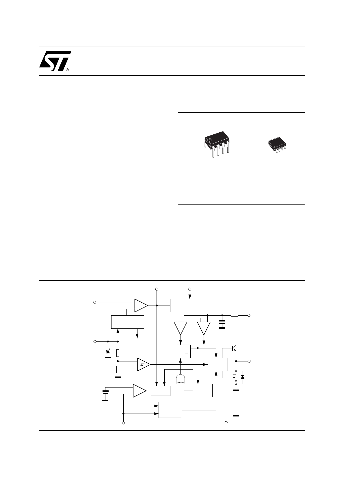
QUASI-RESONANT SMPS CONTROLLER
■ QUASI-RESONANT (QR) ZERO-VOLTAGE-
SWITCHING (ZVS) TOPOLOGY
■ LINE FEED FORWARD TO DELIVER
CONSTANT POWER vs. MAINS CHANGE
■ FREQUENCY FOLDBACK FOR OP TI MU M
STANDBY EFFICI EN CY
■ PULSE-BY-PULSE & HICCUP-MODE OCP
■ ULTRA-LOW START-UP (< 70µA) AND
QUIESCENT CURRENT (< 3.5mA)
■ DISABLE FUNCTION (ON/OFF CONTROL)
■ 1% PRECISION (@ T
REFERENCE VOLTAGE
■ ±400mA TO TE M POLE GATE DR IV E R WI TH
UVLO PULL-DOWN
■ BLUE ANGEL, ENERGY STAR, ENERGY
2000 COMPLIANT
APPLICATIONS
■ TV/MONITOR SMPS
■ AC-DC ADAPTERS/CHARGERS
■ DIGITAL CONSUMER
■ PRINTERS, FAX MACHINES,
PHOTOCOPIERS AND SCANNERS
= 25°C) INTERNAL
j
L6565
DIP8(Minidip) SO-8
ORDERING NUMB ERS :
L6565N L6565D
DESCRIPTION
The L6565 is a current-mode primary controller IC,
specifically designed to build offline Quasi-resonant
ZVS (Zero Voltage Switching at switch turn-on) flyback converters.
Quasi-resonant operation is achieved by means of a
transformer demagnetization sensing input that triggers MOSFET's turn-on.
BLOCK DIAGRAM
January 2003
INV
V
COMP
23
1
2.5V
REGULATOR
CC
20V
R2
2.1V
1.6V
5
VOLTAGE
R1
REF2
V
ZERO CURRENT
Hiccup-mode
ZCD
-
+
INTERNAL
SUPPLY
+
-
DETECTOR
+
-
OCP
UVLO
Blanki ng
BLANKING
DISABLE
START
VFF
LINE VOLTAGE
FEEDFORWARD
2 V
+-
RSQ
Q
STARTER
Starter
STOP
+-
Hiccup-mode
OCP
DRIVER
6
GND
40K
5pF
VCC8
4
CS
7
GD
1/17
Page 2
L6565
DESCRIPTION
(continued)
Converter's power capability variations with the mains voltage are compensated by line voltage feedforward.
At light load the device features a special function that automatically lowers the operating frequency still maintaining the operation as close to ZVS as possible. In addition to very low start-up and quiescent currents, this
feature helps keep low the consumption from the mains at light load and be Blue Angel and Energy Star compliant.
The IC includes also a disable function, an on-chip filter on current sense, an error amplifier with a precise reference voltage for primary regulation and an effective two-level overcurrent protection.
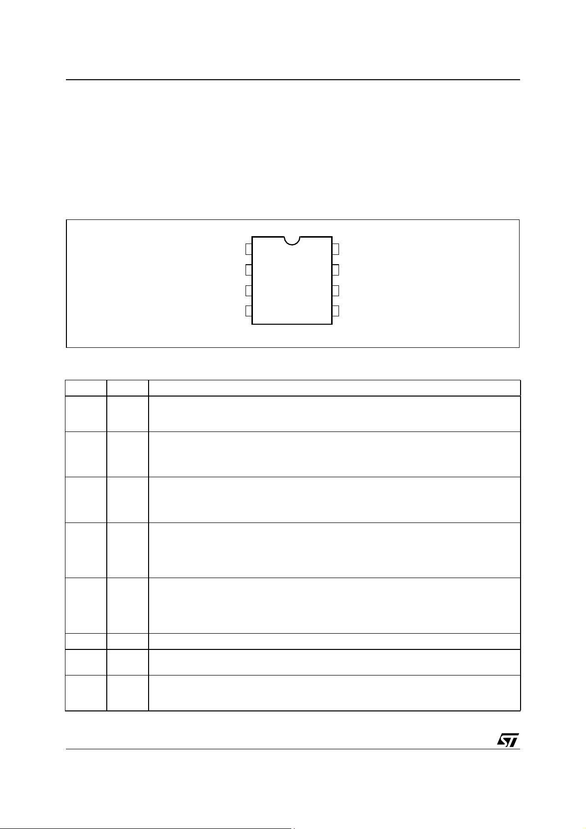
PIN CONNECTION
(Top view, Minidip and SO8)
INV
COMP
VFF
CS
1
2
3
4
Vcc
8
7
GD
GND
6
ZCD
5
PIN DESCRIPTION
N° Name Function
1 INV Inverting input of the error amplifier. The informatio n on the output voltage is fed into the pin
2 COMP Output of the error amplifie r. Typically, a compensat ion network is placed between this pin and
3 VFF Line voltage feedforward. The information on the converter’s input voltage is fed into the pin
4 CS Input to the P WM comparator. The primar y current is sense d through a resistor, the result ing
5 ZCD Transformer’s demagnetization sensing input for Quasi-Resonant operation. Alternately,
6 GND Ground. Current return for both the signal part of the IC and the gate driver.
7 GD Gate d river output. Th e totem pole output stag e is able to d rive power MOSFET ’s and IGBT’s
8 Vcc Supply Voltage of both the signal part of the IC and the gate driver. An electrolytic capacitor is
through either a res istor divider (primary reg ulation) or an optocoupler (second ary feedback).
This pin can be grounded in some secondary feedback schemes (see pin 2).
the INV pin to a chieve stability and good dy namic per forman ce o f the voltage con trol lo op. With
secondar y feedback, the pin can be also driven directly by an optocoupler to control PWM by
modulating the current sunk from the pin (with the INV pin grounded).
through a resistor divider and is used to change the setpoint of the pulse-by-pulse current
limitation (the higher the voltage, the lower the setpoint). If this function is not desired the pin will
be grounded and the current limitation setpoint will be maximum.
voltage is applied to this pin and co mpared with an inter nal reference to determ ine MOSFET’s
turn-off. The inter nal reference is clamped at a value, which defines the pulse-by-pulse current
limitation setpo int, d epen ding on th e voltage at p in VF F. If the sig nal a t the pin C S exceeds 2 V,
the gate driver will be disabled (Hiccup-mode OCP).
synchronizatio n input for an external signal. A nega tive-going edge triggers MO SFET’s turn- on.
The trigger cir cuit is blanked for a minimum of 3 .5 µs after MO SFET tur n-off, for safe operation
under short circuit conditions and frequency foldback. If the pin is grounded the IC will be
disabled.
with a peak current of 400 mA (source and sink).
connected b etween this pin an d ground. A resist or connected from this pin to the converter’s
input bulk capacitor will be typically used to start up the device.
2/17
Page 3
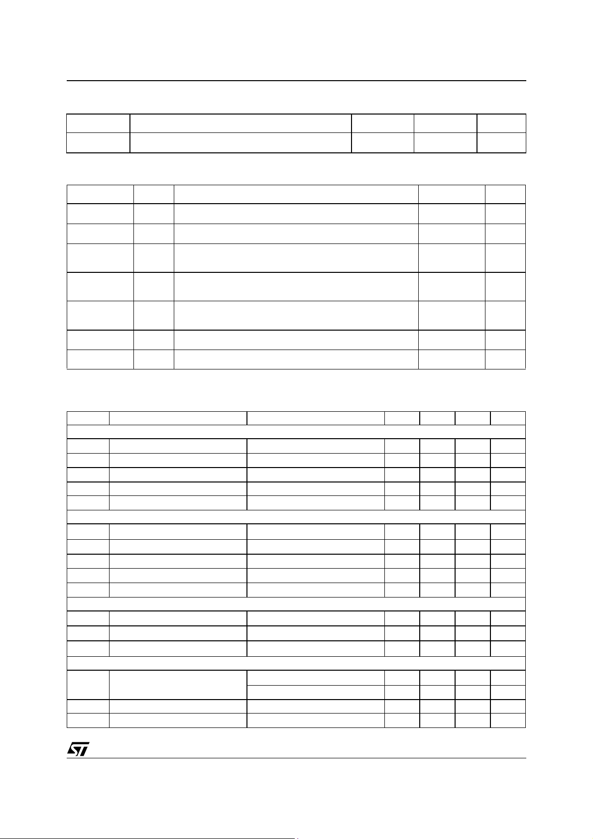
THERMAL DATA
Symbol Parameter SO8 Minidip Unit
L6565
R
th j-amb
Max. Thermal Resistance, Junction-to-ambient 150 100 °C/W
ABSOLUTE MAXIMUM RATINGS
Symbol Pin Parameter Value Unit
I
Vcc
I
GD
INV, COMP,
8ICC + I
Z
7 Output Totem Pole Peak Current (2 µs) ±700 mA
1, 2, 3 4 Analog Inputs & Outputs -0.3 to 7 V
30 mA
VFF, CS
I
ZCD
5 Zero Current Detector 50 (source)
-10 (sink)
P
tot
T
j
T
stg
Power Dissipation @T
= 50°C (Minidip)
amb
(SO8)
1
0.65
Junction Temperature Operating range -40 to 150 °C
Storage Temperature -55 to 150 °C
ELECTRICAL CHARACTERISTCS
(Tj = -25 to 125°C, VCC = 12V, Co = 1nF; unless otherwise specified)
Symbol Parameter Test Condition Min. Typ. Max. Unit
SUPPLY VOLTAGE
V
V
CCOn
V
CCOff
Hys Hysteresis 3.65 4 4.3 V
V
SUPPLY CURRENT
I
start-up
I
LINE FEEDFORWARD
I
VFF
V
VFF
ERROR AMPLIFIER
V
I
INV
Operating range After turn-on 10.3 18
cc
Turn-on threshold 12.5 13.5 14 .5 V
Turn-off threshold 8.7 9.5 10.3 V
Zener Voltage Icc = 25 mA 18 20 22 V
Z
Start-up Current
I
Quiescent Current After turn-on 2.3 3.5 mA
q
Operating Supply Current @ 70 kHz 3.5 5 mA
CC
Quiescent Current During Hiccup-mode OCP 1.6 3.5 mA
I
q
Quiescent Current V
I
q
Input Bias Current V
Before turn-on, V
< V
ZCD
VFF
, VCC>V
DIS
= 0 to 3 V -1 µA
CC
= 12V
CCOff
45 70 µA
1.4 2.1 mA
Operating Range 0 to 3 V
K Gain
Voltage Feedback Input
INV
Threshold
V
= 1.5V, V
VFF
T
= 25°C 2.465 2.5 2.535 V
amb
COMP
= 4V
12V < VCC < 18V 2.44 2.56
0.16
Line Regulation Vcc = 12 to 18V 2 5 mV
Input Bias Current -0.1 - 1 µA
mA
W
3/17
Page 4
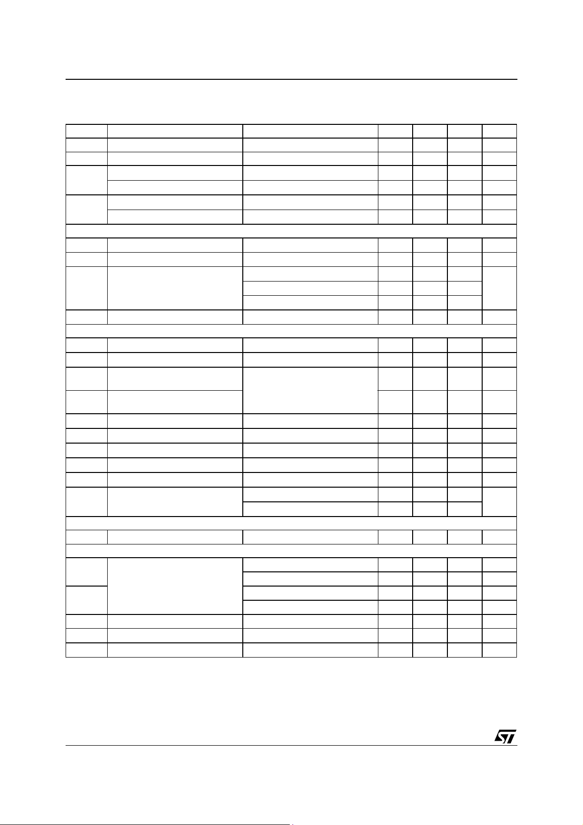
L6565
ELECTRICAL CHARACTERISTCS
(T
= -25 to 125°C, VCC = 12V, Co = 1nF; unless otherwise specified)
j
(continued)
Symbol Parameter Test Condition Min. Typ. Max. Unit
G
Voltage Gain Open loop 60 80 dB
V
GB Gain-Bandw idth Produ ct 1 MHz
I
COMP
V
COMP
Source Current V
Sink Current V
Upper Clamp Voltage I
Lower Clamp Voltage I
= 4V, V
COMP
= 4V, V
COMP
SOURCE
SINK
= 0.5 mA 5 5.5 V
= 0.5 mA 2.25 2.55 V
= 2.4 V -2 -3.5 -5 mA
INV
= 2.6 V 2.5 4.5 mA
INV
CURRENT SENSE COMPARATOR
I
t
d(H-L)
V
V
CSdis
Input Bias Current VCS = 0 -0.05 -1 µA
CS
Delay to Output 200 450 ns
Current Sense Reference Clamp
CSx
V
= Upper clamp, V
COMP
V
= Upper clamp, V
COMP
V
= Upper clamp, V
COMP
VFF
VFF
VFF
= 0V
= 1.5V
= 3V
1.28 1.4 1.5 V
0.62 0.7 0.78
00.2
Hiccup-mode OCP level 1.85 2.0 2.2 V
ZERO CURRENT DETECTOR/ SYNCHRONIZATION
V
ZCDH
V
ZCDL
V
ZCDA
Upper Clamp Voltage I
Lower Clamp Voltage I
Arming Voltage
= 3mA 4.7 5.2 6.1 V
ZCD
= - 3mA 0.3 0.65 1 V
ZCD
(1)
2.1 V
(positive-going edge)
V
ZCDT
Triggering Voltage
1.6 V
(negative-going edge)
I
ZCDb
I
ZCDsrc
I
ZCDsnk
V
I
ZCDr
T
BLANK
Input Bias Current V
= 1 to 4.5 V 2 µA
ZCD
Source Current Capability -3 -10 mA
Sink Current Capability 3 10 mA
Disable Threshold 150 200 250 mV
DIS
Restart Current After Disable V
Blanking time after pin 7 high-to-
low transition
ZCD
V
COMP
V
COMP
< V
, Vcc > Vcc
DIS
off
-70 -150 -230 µA
≥ 3.2 V 3.5 µs
= 2.5 V 18
START TIMER
t
START
Start Timer period 250 400 550 µs
GATE DRIVER
V
OL
V
OH
t
f
t
r
I
GDoffIGD
Dropout Voltage I
GDsource
I
GDsource
I
GDsink
I
GDsink
Current Fall Time 40 100 ns
Current Rise Time 40 100 ns
sink current Vcc = 4 V, VGD = 1 V 5 10 mA
= 200mA 1.2 2 V
= 20mA 0.7 1
= 200mA 2 V
= 20mA 0.3
(1) Parame ters guaran teed by design, not tested i n production.
4/17
Page 5
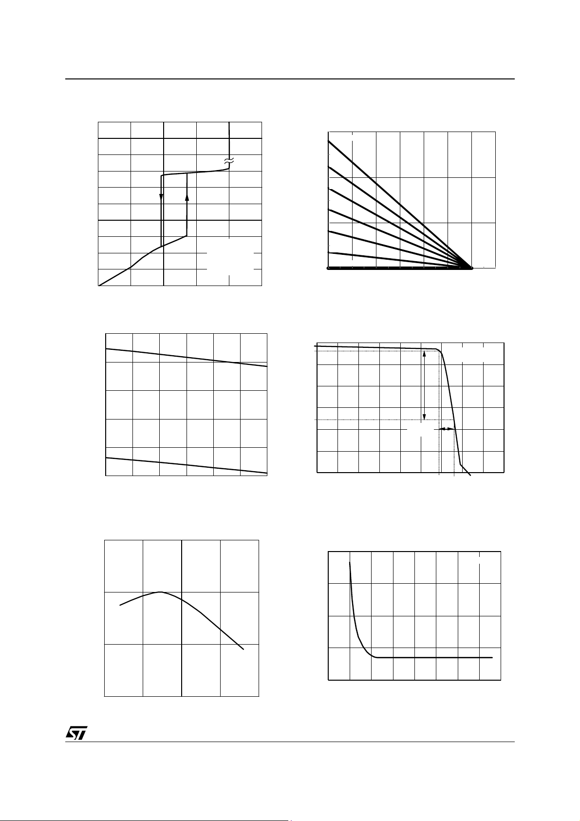
L6565
(V)
Figure 1. Supply current vs. Supply voltage
CC
I
(mA)
10
5
1
0.5
0.1
0.05
0.01
0.005
CL = 1nF
f = 70KHz
TA = 25°C
0
0 5 10 15 20 V
CC
Figure 2. Start - up & U VL O vs . Tem perature
14
V
CC-ON
(V)
13
Figure 4. Line feedforward characteristics
V
[V]
csx
1.5
Upper clamp
5.0 V
1
4.5 V
4.0 V
0.5
3.5 V
3.0 V
VCOMP = 2.5V
0
0 0.5 1 1.5 2 2.5 3 3.5
V
[V]
VFF
Figure 5. Pin 2 (COMP) V-I characteristics
V
[V]
COMP
6
5
Tj = 25 °C
Vpin1 = 0
12
11
10
V
CC-OFF
(V)
9
-25 0 25 50 75 100 125
T (°C)
Figure 3. Fee dback referen ce v s. Te m pe rature
V
REF
(V)
2.50
2.48
D94IN048A
4
3
2
Regulation
range
1
0
01234
I
[mA]
COMP
Figure 6. ZCD blanking time vs. COMP voltage
T
[µs]
BLANK
20
15
10
5
Tj = 25 °C
2.46
-50 0 50 100
T (°C)
0
23456
V
[V]
COMP
5/17
Page 6
L6565
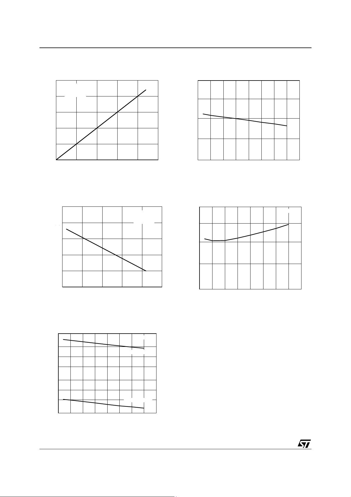
Figure 7. Gate-drive output saturation
V
[V]
pin7
2.5
Tj = 25 °C
Vcc = 14.5 V
2
SINK
1.5
1
0.5
0
0 100 200 300 400 500
IGD[mA]
Figure 8. Gate-drive output saturation
V
[V]
pin7
0
Vcc - 0.5
Vcc - 0.5
-0.5
Tj = 25 °C
Vcc = 14.5 V
SOURCE
Figure 10. Zener voltage at Vcc pin vs. Tj
Vz [V]
22
21
20
19
18
-50 0 50 100 150
Tj [°C]
Figure 11. Start-up timer period vs. Tj
TSTART [µs]
450
400
Vcc=12V
Vcc - 1.0
-1
-1.5
Vcc - 1.5
Vcc - 2.0
-2
Vcc - 0.5
-2.5
0 100 200 300 400 500
IGD[mA]
Figure 9. IC co nsumption vs . te m perature
Icc [mA]
5
2
1
0.5
0.2
0.1
0.05
Vcc=12V
Quiescent
Before Start-up
350
300
250
-50 0 50 100 150
Tj [°C]
0.02
-50 0 50 100 150
Tj [°C]
6/17
Page 7
L6565
APPLICATION INFORMATION
Quasi-resonant oper ation i n offli ne fly back converter s lies in synchronizing MO SFET's turn-on to the transformer's demagnetization. Detecting the resulting negative-going edge of the voltage across any winding of the
transformer can do this. The L6565 is provided with a dedicated pin that allow s doing the job with a ver y simple
interface, just one resistor.
Variable frequency operation - as a result of different operating conditions in terms of input voltage and output
current - is inherent in such functionality. The system always works close to the boundary between DCM (Discontinuous Conduction Mode) and CCM (Continuous Conduction Mode) operation of the transformer. The operation is then identical to that of the so-called self-oscillating or Ringing Choke Converter (RCC).
Detailed Device Description
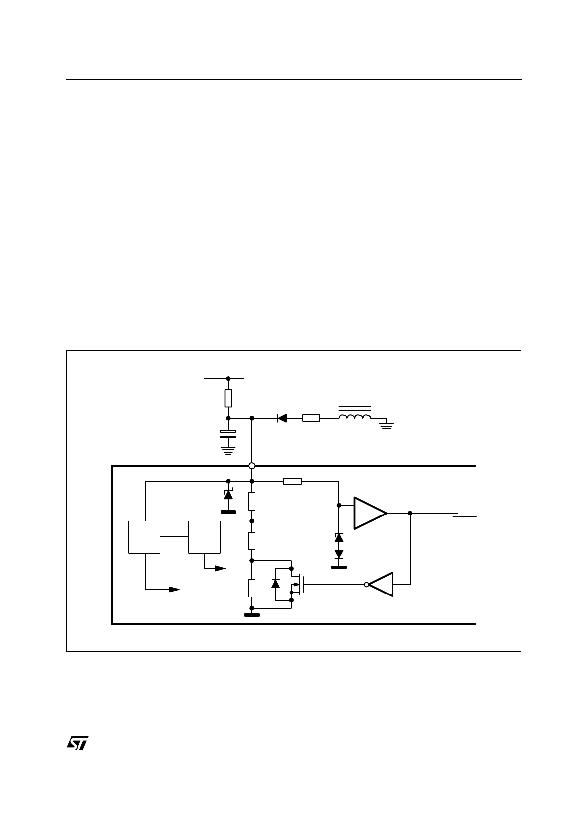
Internal Supply Block (see fig. 12)
A linear voltage regulator supplied by Vcc (pin 8) generates an internal 7V rail used for supplying the entire IC,
except for the gate driver that is supplied directly from Vcc. In addition, a bandgap circuit generates a precise
internal reference (2.5V±1% @ 25°C) used by the control loop to ensure a good regulation with primary feedback technique.
In figure 12 it is also shown the undervoltage lockout (UVLO) comparator with hysteresis used to enable the
chip as long as the Vcc voltage is high enough to ensure a reliable operation.
Figure 12. L6565 internal supply block
LIN.
REG.
7V bus
+Vin
REF.
2.5V
Vcc
8
-
+
UVLO
7/17
Page 8
L6565
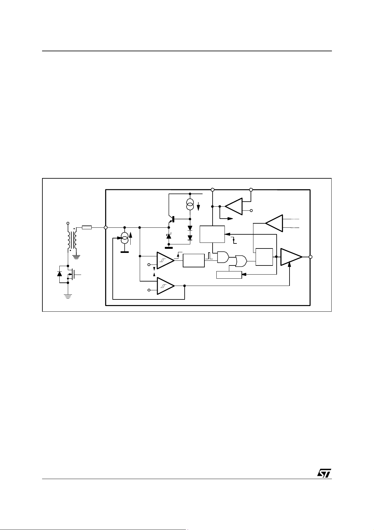
Zero Current Detection and Triggering Block (see fig. 13):
The Zero Current Detection (ZCD) block switches on the external MOSFET if a negative-going edge falling below 1.6 V i s ap plied to the input (pin 5, ZCD) . However, to en sur e hig h nois e im munity, the trigge ring blo ck must
be armed first: prior to falling below 1.6V, the voltage on pin 5 mus t experience a positive-going edge exc eeding
2.1 V.
This feature is typically used to detect transformer demagnetization for QR operation, where the signal for the
ZCD input is obtained from the transfor mer' s auxiliar y winding us ed also to s upply the IC. A lternativel y, this can
be used to synchronize MOSFET's turn-on to the negative-going edge of an external clock signal, in case the
device is not required to work in QR mode but as a standard PWM controller in a synchronized system (e.g.
monitor SMPS).
The triggering block is blanked for a certain time after the MOSFET has been turned off. This has two goals:
first, to prevent any negative-going edge that follows leakage inductance demagnetization from triggering the
ZCD circuit erroneously; second, to realize the Frequency Foldback function (see the relevant description).
Figure 13. Zero Current Detection and Triggering Block; Disable and Frequency Foldback Blocks
INVCOMP
L6565
+Vin
Q
ZCD
R
ZCD
5
MONO
STABLE
BLANKING
TIME
STARTER
150µA
0.2V
0.3V
1.6V
2.1V
5.2V
-
+
-
+
DISABLE
E/A
to line
FFWD
-
+
blanking
START
2.5V
starter STOP
PWM
R
Q
S
DRIVER
7
GD
A circuit is needed that turns on the external MOSFET at start-up since no signal is coming from the ZCD pin.
This is realized with an internal starter, which forces the driver to deliver a pulse to the gate of the MOSFET.
To minimize the external interface with the synchronization source (either the auxiliary winding or an external
clock), the voltage at the pin is both top and bottom limited by a double clamp, as illustrated in the internal diagram of the ZCD block of figure 13. The upper clamp is typically located at 5.2 V, while the lower clamp is at
one V
above ground. The interface will then be made b y just one res istor that has to l imit the c urrent s ourced
BE
by and sunk from the pin within the rated capability of the internal clamps.
Disable Block (see fig. 13):
The ZCD pin is used also to activate the Disable Block. If the voltage on the pin is taken below 150 mV the device will be shut down. To do so, it is necessary to override the source capability (10 mA max.) of the internal
lower clamp. While in disable, the current consumption of the IC will be reduced. To re-enable device operation,
the pull-down on the pin must be released.
Frequency Foldback Block (see fig. 13):
To prevent the switching frequenc y fr om reac hing too high val ues, w hich is a typical drawback of QR operation,
8/17
Page 9
L6565
00000000
0
00000
0
00000
0
00000
0
00000
0
00000
00000000
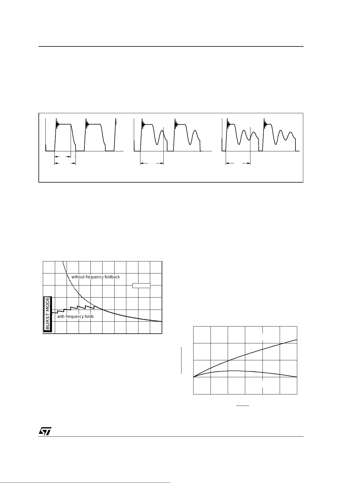
the L6565 puts a limit on the minimum OFF-time of the switch. This is done by blanking the triggering block of
the ZCD circuit as mentioned before. The duration of the blanking time (3.5µs min.) is a function of the error
amplifier output VCOMP, as shown in the diagram of figure 6.
If the load current and the input voltage are such that the switch OFF-time falls below the minimum blanking
time of 3.5µs, the system will enter the "Frequency Foldback" mode, a sort of "r ingi ng cycl e ski pping" ill ustr ated
schematically in figure 14.
Figure 14. Frequency foldback: ringing cycle skipping as the load is progressively reduced
V
DS
TFW
TV
T
BLANKmin
Pin = Pin'
(limit condition)
V
DS
t
T
BLANK
Pin = Pin'' < Pin' Pin = Pin''' < Pin''
V
DS
t
T
BLANK
t
In this mode, uneven switching cycles may be observed under some line/load conditions, due to the fact that
the OFF-time of the MOSFET is allowed to change with discrete steps (2·Tv), while the OFF-time needed for
cycle-by-cycle energy balance may fall in between. Thus one or more longer switching cycles will be compensated by one or more shorter ones and vice versa. However, this mechanism is absolutely normal and there is
no appreciable effect on the performance of the converter or on its output voltage.
Figure 15. Frequency Foldback: qualitative
freque ncy dependen ce on po we r
throughput
f
sw
Voltage Feedforward block (see fig. 17b):
The power that QR flyback converters with a fixed
overcurrent setpoint (like fixed-frequency systems)
are able to deliver changes with the input voltage
considerably. With wide-range mains, at maximum
line it can be more than twice the value at minimum
without frequency foldback
Vin fixed
line, as shown by the upper curve in the diagram of
figure 16. The L6565 has the Line Feedforward function available to solve this issue.
00
00
00
00
with fr equency foldback
00
BURST MODE
Pin
Further load reductions involve lower values for
VCOMP, which increases the blanking time. Therefore, more and more ringing cycles will be skipped.
When the load is low enough , so many ringing cycles
need to be skipped that their amplitude becomes
very small and they can no longer trigger the ZCD circuit. In that case the internal starter of the IC will be
activated, resulting in burst-mode operation: a series
of few switching cycles spaced out by long periods
where the MOSFET is in OFF state.
Figure 16. Typical power capability change vs.
input voltage in ZVS QR flyback
convert e rs
2.5
system no t
Vin
Vinmin
compens ated
system o ptimally
compensated
2
in
@ V
1.5
inlim
P
Pinlim @ Vinmin
1
0.5
11.522.533.54
9/17
Page 10
L6565
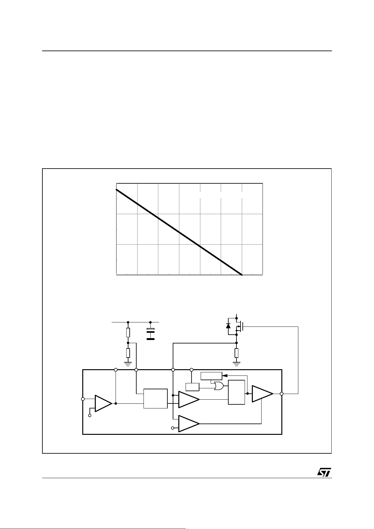
It acts on the clamp level of the control voltage V
, that is on the overcurrent setpoint, so that it is a function
csx
of the converter's input v oltage sensed through a dedi cated pin (#3 , VFF): the higher the input v oltage, the lower
the setpoint. This is illustrated in the diagram of figure 17a that shows the relationship between the voltage at
the pin VFF and V
(with the error amplifier saturated high in the attempt of k eeping output voltage regul ation).
csx
The schematic in figure 17b shows also how the function is included i n the control loop. With a pr oper selec tion
of the external divider R1-R2 it is possible to achieve the optimum compensation described by the lower curve
in the diagram of figure 16.
In applications wher e this fun ction is not w anted, e.g. bec ause of a na rrow input v oltage range, the VFF pin can
be simply grounded, thus sav ing t he resis tor div ider. The overcur rent setpoint wi ll be then fixed at th e maxi mum
value of about 1.4V (1.5V max.).
Line Feedforward is also beneficial to other characteristics of quasi-resonant converters: it improves their input
ripple rejection ability and limits the variation of the power stage's small-signal gain versus the line voltage.
Figure 17. a) Overcurrent se tpoint vs. VFF vol ta ge; b) Line Feedforward function block
V
[V]
csx
1.5
VCOMP = Upper clamp
1
0.5
a)
INV
0
0 0 .5 1 1.5 2 2.5 3 3.5
+Vin
R1
R2
COMP VFF CS
23
1
E/A
+
2.5V
VOLTAGE
FEED
FORWARD
2 V
V
[V]
VFF
Rs
ZCD
4
5
STARTER
ZCD
+
PWM
-
+
Hiccup
-
starter STOP
S
R
(reset-dominant)
DISABLE
Q
DRIVER
7
GD
L6565
b)
10/17
Page 11
L6565
Error Amplifier Block (see fig. 17b):
The Error Amplifier (E/A) inverting input is used in primary feedback technique to compar e a partition of the voltage generated by the auxiliary winding with the internal reference, to achieve converter's output voltage regulation (see "Applica tion Ideas ", fig. 24) . With secondary feedback (t ypi cally usi ng a TL4 31 at the sec ondary s ide
and an optocoupler to transfer output voltage information to the primary side through the isolation barrier) the
E/A can be used as an inverting level-shifter to achieve negative feedback and shape the loop gain (see "Application Ideas", fig. 23).
The E/A output is used typically for control loop compensation, realized with an RC network connected to the
inverting input. With other secondary feedback techniques, the output is driven directly by an emitter-grounded
optocoupler to modulate the duty cycle (the inverting input will be grounded in that case - see figure 23 in "Application Ideas").
Current Comparator, PWM Latch and Hiccup-mode OCP (see fig. 17b):
The current comparator senses the voltage ac ross the cur rent sens e resistor ( Rs) and, by com paring it with the
programming signal deliver ed by the feedforwar d block, determi nes the exact ti me when the external MOSFET
is to be switched off. The PWM latch avoids spurious switching of the MOSFET, which might result from the
noise generated ("double-pulse suppression").
A comparator senses the voltage on the current sense input and disables the gate driver if the voltage at the pin
exceeds 2 V. Such anomalous condition i s typically generated by a short circuit on the secondary rec tifier or on
the secondary winding. To re-enable the driver, first the IC must be turned off and then can be restarted, that is
the Vcc voltage must fall below the UVLO threshold.
When the gate driver is disabled the quiescent current of the IC is unchanged and, since no energy is coming
from the self-supply circuit, the Vcc capacitor will be discharged below the UVLO threshold after some time.
Then the device will initi ate a new start-up cyc le. In case of failure of the seco ndary diode the resul ting beh avior
will be a low-frequency intermittent oper ation (Hiccup-mode operation), wi th very low stress on the power circuit.
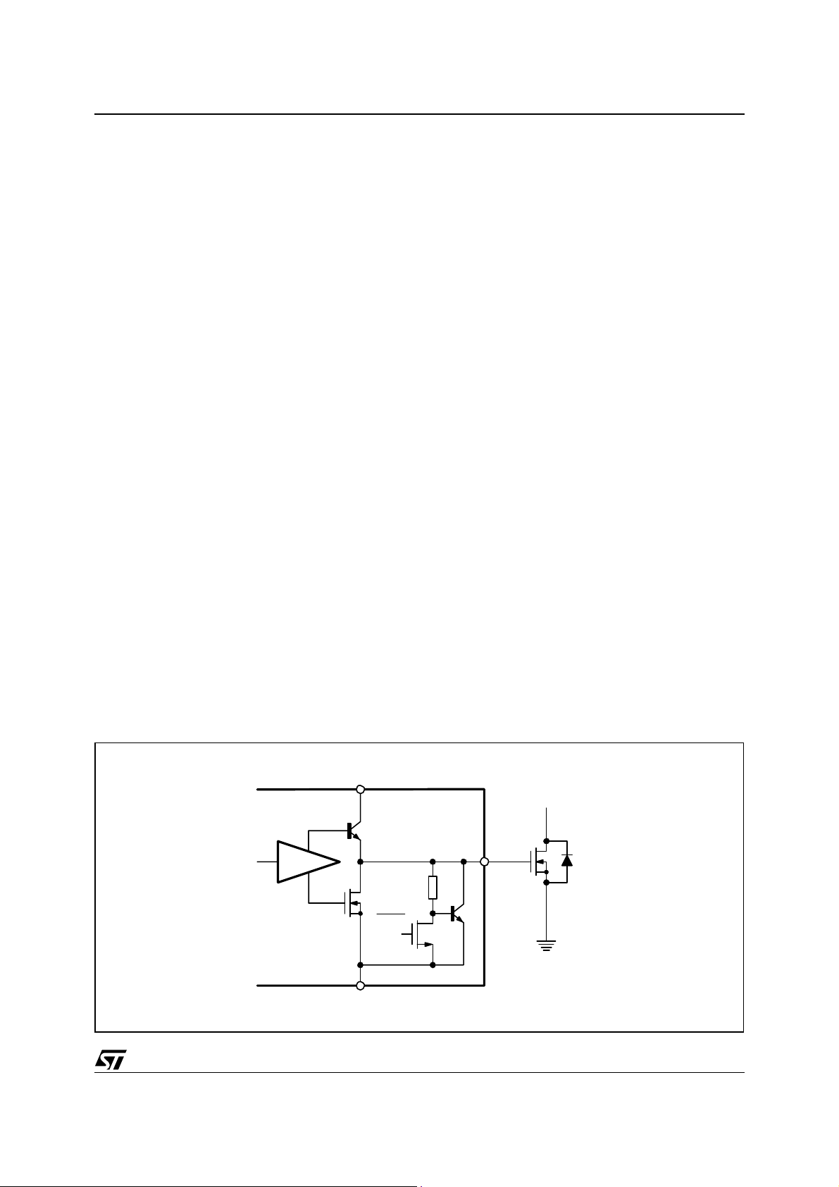
Gate Driver (see fig. 18):
A totem pole buffer, with 400mA source and sink capability, drives the external MOSFET. It is made up of a
high-side NPN Darlington and a low-side MOSFET. In this way there is no need of an external diode clamp to
prevent the voltage at the gate drive output (pin 7, GD) from being pulled too negative.
An internal pull-down circuit holds the output low when the device is in UVLO conditions, to ensure that the external MOSFET cannot be turned on accidentally (e.g. at power-on).
Figure 18. Gate driver with UVLO pull-down
Vcc
8
L6565
7
GD
DRIVER
UVLO
6
GND
Q
11/17
Page 12
L6565
TYPICAL APPLICATIONS
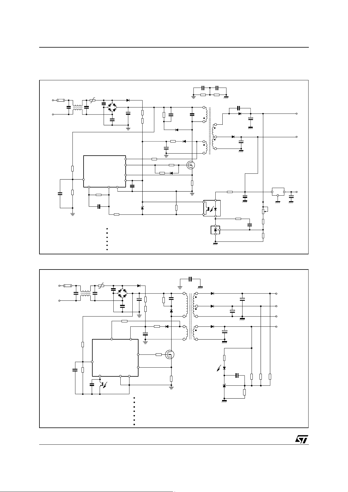
Figure 19. 50W Wide Range Mains SMPS for 14" TV
15mH
NTC1
16R
C25
1nF
C24
100nF
L1
IC1
VFF
L6565
3
2
COMP
1
R12
47 k
C5
2.2 nF
TRANSFORMER SPECS:
CORE: ETD29x16x1 0, N67 mate ri al or equivalent
≈
N1: 48 T (24T+24T se r i es connected), 2xAWG28 (
N2: 31 T, AWG28
N3: 5 T, AWG28
Naux: 5 T, AWG32 (∅0.24 mm)
D1
1N4148
B1 2KBP04M
C1
R13
3.3 k
R1
µ
F
150
400 V
C26
1nF
ZCD
5
GD
7
CS
4
Vcc
8
6
C27
220nF
GNDINV
75k
R2
75k
DZ1
15 V
R20 22 k
100 k
R5
R7 10
C8
8.2 nF
250 V
D3 STTA10 6
R8 22
C4
47
µF
25V
R6 100
D2
1N4148
1 mm air gap for a primary inductance of 285 µH
Vin
88 to
264 Vac
1 nF
C3
F1
2A fuse
C23
100nF
R3
3 M
16 K
R4
1N4148
R14
1.5 k
180 pF
C6 4700pF/ 4KV
C2
630V
D4
R11
0.47
0.37 mm)
∅
R9
4.7M
N1
Naux
Q1
STP7NB80FI
IC3 PC817
4
3
IC2 TL431
3
1
4
5
C7 4700pF/ 4KV
R10
4.7M
T1
8
N2
9
N3
10
1
2
1
2
3
BYT01-400
D6
BYW98-100
R15
1.8 k
C22
100 pF
D5
R16
220 k
C13
100 nF
C10
470 µF
25 V
100 µF 25V
220 µF
C12
C9
160 V
100 k
150 k
R17
4.7 k
P1
R18
105 V
0.35 A
14 V
1 A
+5 V
IC4
3
50 mA
C11
47 µF
25V
12
L7805
Figure 20. 40W Wide Range Mains SMPS for inkjet printer
2200pF 4KV
15mH
3.3 nF
16 k
16R
1nF
L6565
3
Ω
2
1
47 k
1N4148
2KBP04M
1nF
Ω
85
6
Ω
0.39 Ω
Ω
1N4148
Ω
1/2 W
10 nF
250V
N1
STP4NA80FP
Ω
75 k
56 k
2 W
Ω
75 k
STTA106
10
µ
47
F
7
4
10
PC817
TRANSFORMER SPECS:
CORE: ETD29x16x10, 3C85 material or equivalent
≈
1 mm air gap for a primary inductance of 700 µH
N1: 75 T, AWG25 (
N2: 8 T, AWG25
N3: 7 T, AWG20 (∅0.89 mm)
N4: 3 T, AWG25
N5: 7 T, AWG32 (∅0.24 mm)
∅
0.51 mm)
2A fuse
Vin
88 to
100nF 100nF
264 Vac
3 M
10 nF
Ω
BYW100-200
2 x 470µF
N2
BYW98-100
N3
N4N5
2 x 1000µF
BYW100-50
Ω
220
16V
470µF
16V
35V
28V / 0.7A
12V / 1.5A
GND
5V / 0.5A
PC817A
TL431
100 nF
2.7 k
Ω
3.9 k
Ω
5.1 k
Ω
270 k
Ω
12/17
Page 13
L6565
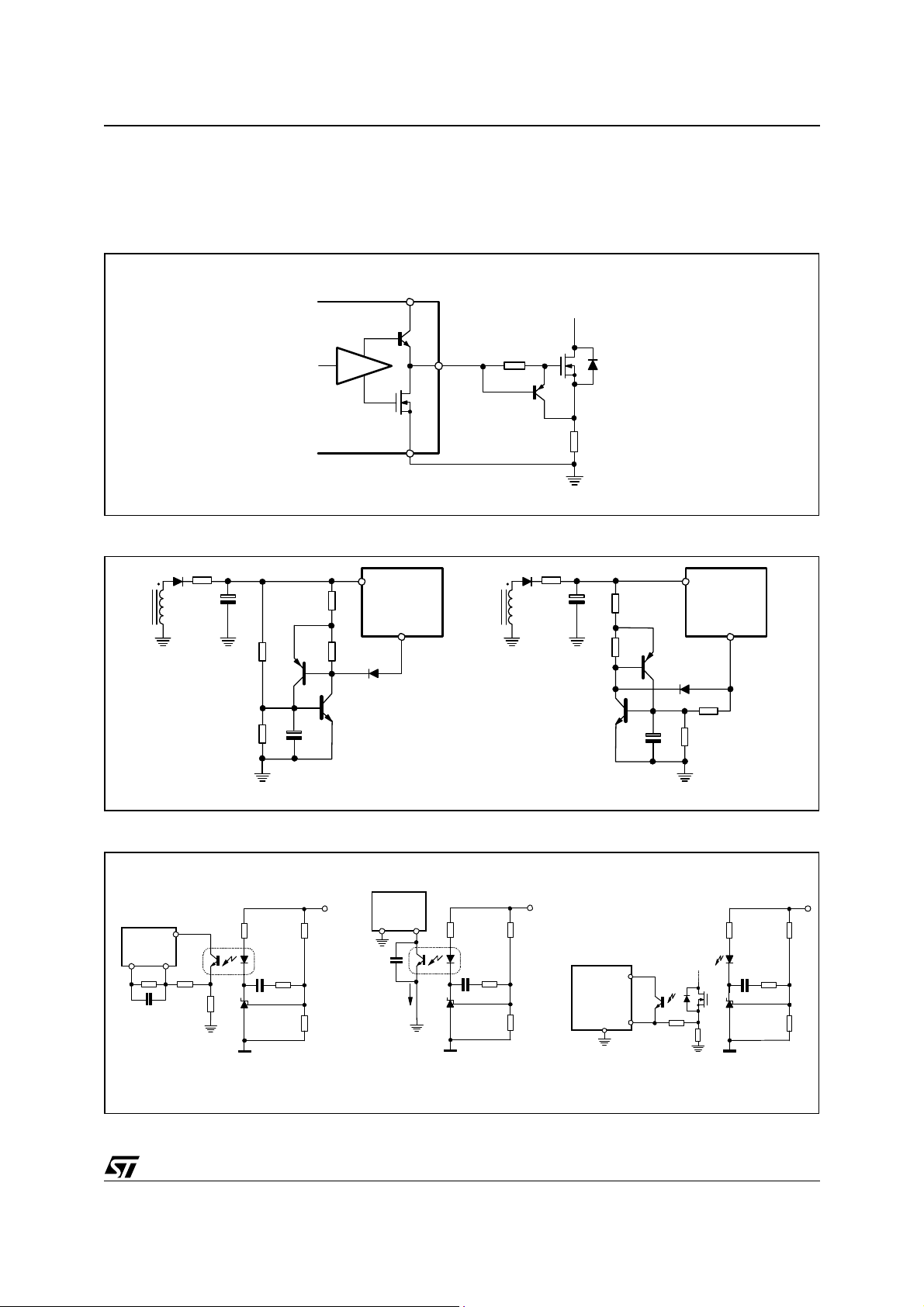
APPLICATION IDEAS
Here follows a series of ideas/suggestions aimed at either improving performance or solving common application issues of L6565-based power supplies.
Figure 21. Enhanced t urn-off f or big MOSFET's dr ive
Vcc
8
7
DRIVER
GD
BC327
Q
L6565
6
Rs
GND
Figure 22. Latched shutdown on: a) feedback disconnection; b) overload or short circuit
BC327
a)
Vcc
BC337
8
L6565
2
COMP
1N4148
BC337
b)
Vcc
BC327
1N4148
8
L6565
2
COMP
Figure 23. Secondary Feedback loop configurations
COMP
L6565
R
A
Vout
Vcc
8
12
INV
R
B
TL431
L6565
1
ICOMP
2
COMPINV
TL431
Vout
L6565
1
INV
Vout
Vcc
8
4
CS
Roff
TL431
Rs
a) b) c)
13/17
Page 14
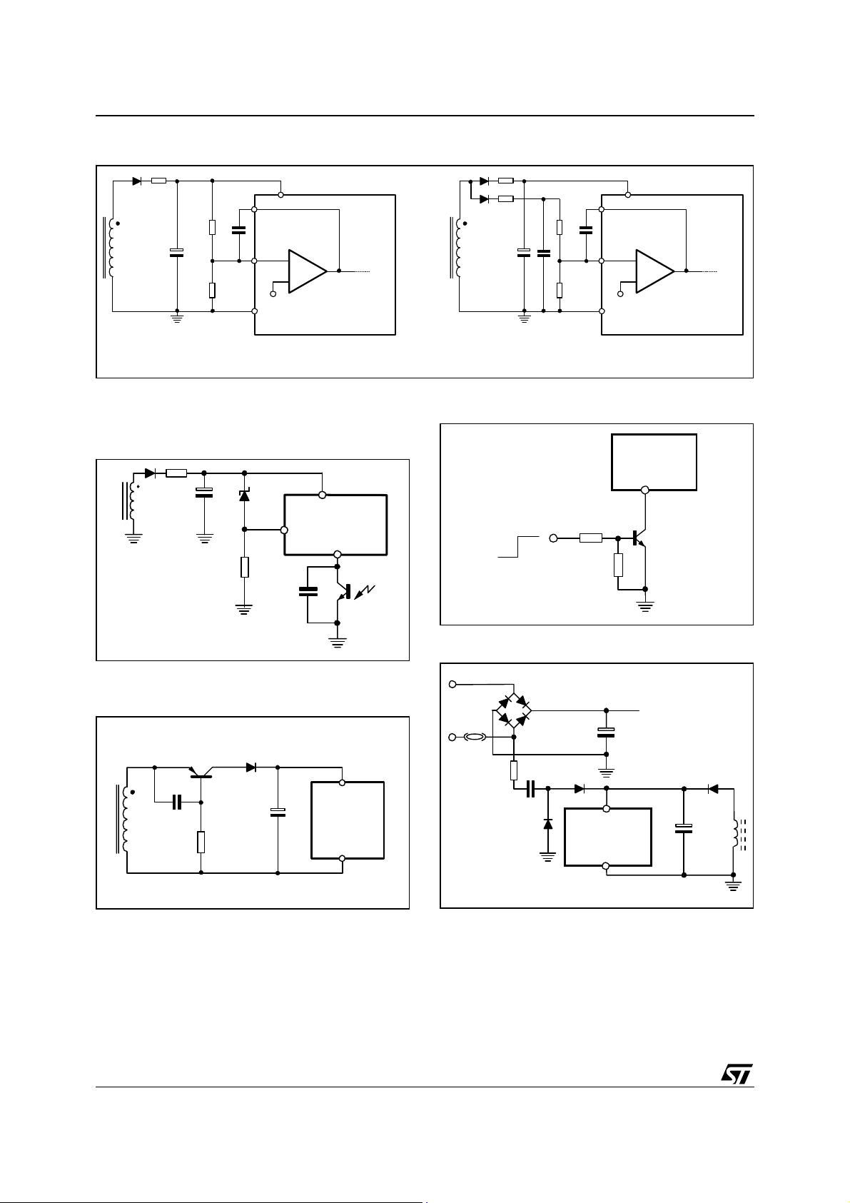
L6565
Figure 24. Primary Feedbac k loop conf igura tions
Vcc
8
2
1
-
E/A
+
2.5V
6
L6565
R
R
COMP
H
INV
L
GND
a)
Figure 25. Protection against secondary
feedback disconnection by primary
regulation take-over
1
Vcc
8
L6565
2
COMP
15 V
INV
2.2 kΩ
to VFF
block
Vcc
8
2
1
-
E/A
+
2.5V
6
R
R
COMP
H
INV
L
GND
b)
Figure 27. Remote ON/OFF control
L6565
5
ZCD
OFF
ON
BC337
L6565
to VFF
block
Figure 28. Low-consumption start-up circuit
Figure 26. Le adi ng ed ge bl anking circui t for
enhanced primary regulation
1N4148BC327
470 pF
2.7 k
Ω
L6565
Vcc
GND
Vac
R
1N4148
CSTART
1N4148
6
GND
Vcc
8
L6565
+Vin
C
SUPPLY
RELATED DOCUMENTATION
[1] "L6565, QUASI-RESONANT CONTROLLER” (AN1326)
[2] “25W QUASI-RESONANT FLYBACK CONVERTER FOR SET-TOP BOX APPLICATIONS USING THE
L6565” (AN1376)
[3] “EVAL6565N, 30W AC-DC ADAPTER WITH THE L6565 QUASI-RESONANT PWM CONTROLLER”
(AN1439).
14/17
Page 15
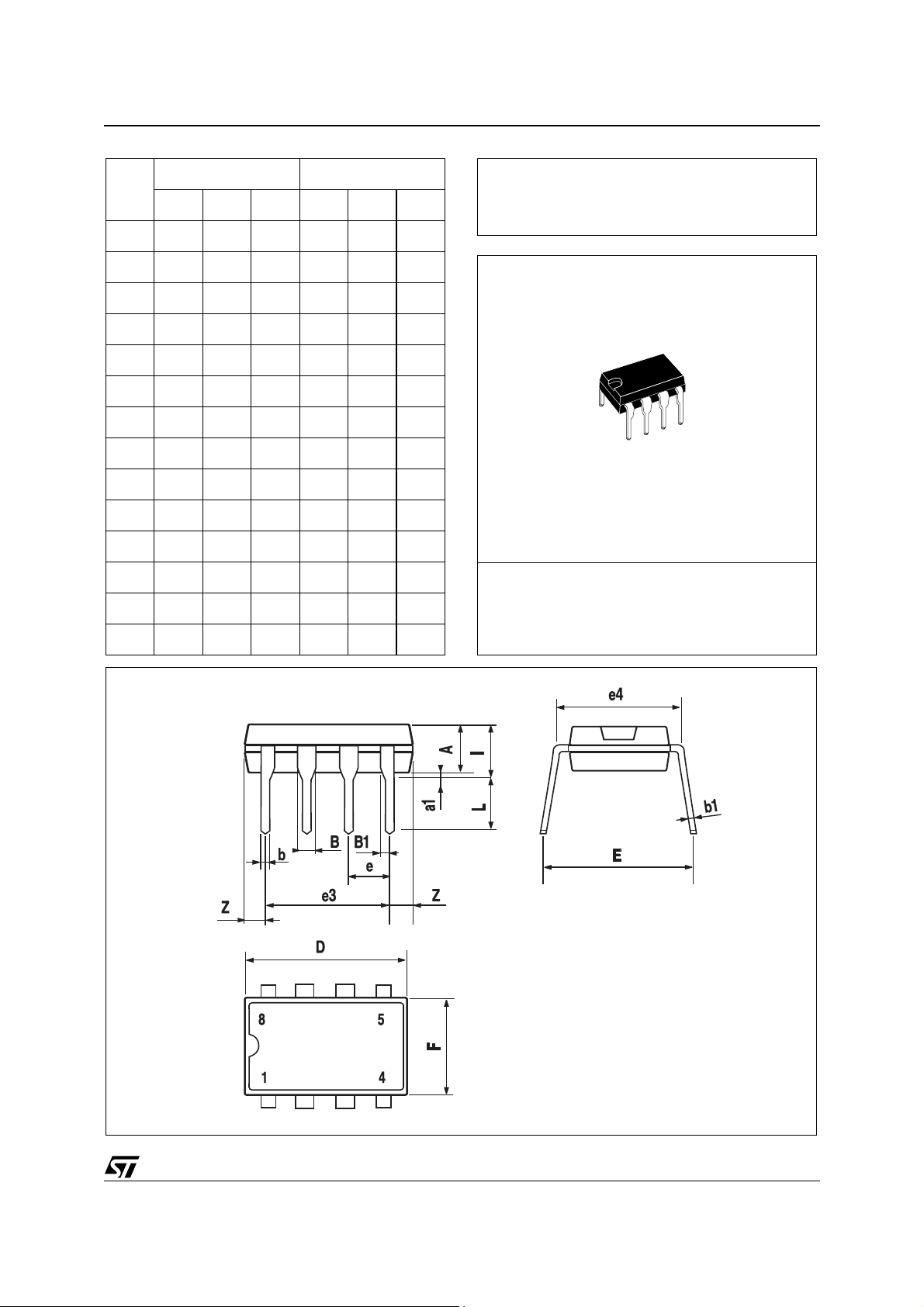
mm inch
DIM.
MIN. TYP. MAX. MIN. TYP. MAX.
A 3.32 0.131
a1 0.51 0.020
B 1.15 1.65 0.045 0.065
b 0.356 0.55 0.014 0.022
b1 0.204 0.304 0.008 0.012
D 10.92 0.430
E 7.95 9.75 0.313 0.384
e2.54 0.100
e3 7.62 0.300
e4 7.62 0.300
F 6.6 0.260
L6565
OUTLINE AND
MECHANICAL DATA
I 5.08 0.200
L 3.18 3.81 0.125 0.150
Z 1.52 0.060
Minidip
15/17
Page 16
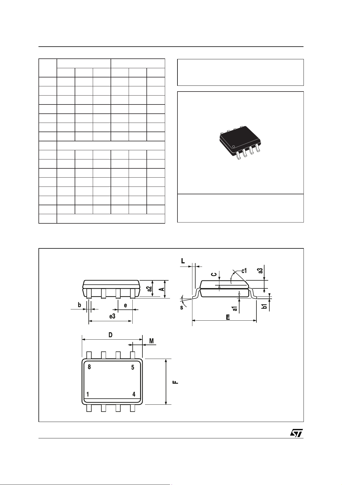
L6565
DIM.
D (1) 4.8 5.0 0.189 0.197
F (1) 3.8 4.0 0.15 0.157
(1) D and F do not include mold flash or protrusions. Mold flash or
potrusions shall not exceed 0.15mm (.006inch).
MIN. TYP. MAX. MIN. TYP. MAX.
A 1.75 0.069
a1 0.1 0.25 0.004 0.010
a2 1.65 0.065
a3 0.65 0.85 0.026 0.033
b 0.35 0.48 0.014 0.019
b1 0.19 0.25 0.007 0.010
C 0.25 0.5 0.010 0.020
c1 45° (typ.)
E 5.8 6.2 0.228 0.244
e 1.27 0.050
e3 3.81 0.150
L 0.4 1.27 0.016 0.050
M 0.6 0.024
S8° (max.)
mm inch
OUTLINE AND
MECHANICAL DATA
SO8
16/17
Page 17

L6565
Information furnished is believed to be accurate and reliable. However, STMicroelectronics assumes no responsibility for the consequences
of use of such information nor for any infringement of patents or other rights of third parties which may result from its use. No license is granted
by implic ation or o th erwise un der any pat ent or patent right s of STMicroelectronics. Specifications me ntioned in this publication are subject
to change without notice. This publication supersedes and replaces all information previously supplied. STMicroelectronics products are not
authoriz ed f or use as crit i cal components in life support dev i ces or systems wi thout exp ress written approval of STMicroel ectronics.
The ST logo is a registered trademark of STMicroelectronics
©
2003 STMicroelec tr onics - All Rights Rese rved
Australia - Brazi l - Canada - Ch i na - F i nl and - Franc e - Germany - Hong Kong - In di a - Israel - Italy - Japan -Malaysia - Malta - Morocco -
Singap ore - Spain - Sw eden - Switzerland - Un i t ed Kingdom - United St at es.
STMicroelectronics GROUP OF COMPANIES
http://www.s t. com
17/17
 Loading...