

Page 1
L6280
THREE CHANNELS MULTIPOWER DRIVER SYSTEM
ADVANCE DATA
PROGRAMMABLE CONFIGURATION
(CHANNELS1 AND2)
OUTPUT CURRENT UP TO 1A (CHANNELS
1AND2)
1 SENSEPER CHANNEL
OUTPUTCURRENT CHANNEL 3 UP TO 3A
DIRECT INT ERFACE TO MICROP ROCESSOR
C-MOSCOMPATIBLE INPUT
INTERNAL DC-DC CONVERTER FOR LOGIC
SUPPLY(+5V)
POWER FAIL
WATCHDOG MANAGEMENT
THERMAL PROTECTION
VERY LOW DISSIPATED POWER (SUIT-
ABLE FOR USE IN BATTERY SUPPLIED APPLICATIONS)
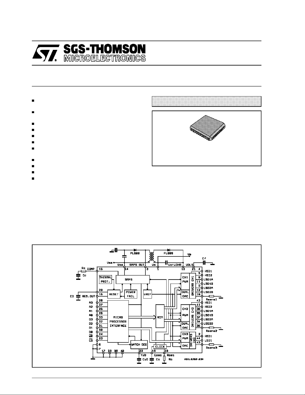
DESCRIPTION
TheL6280 is a multipowerdriver system for motor
and solenoid control applicatios that connects directly to a microprocessor bus. Realized in MultipowerBCD technology-- which combinesisolated
DMOS transistors, CMOS & bipolar circuits on the
BLOCK DIAGRAM
MULTIPOWERBCD TECHNOLOGY
PLCC44
ORDERING NUMBER: L6280
same chip -- it integrates two 1A motor drivers
(channels1 & 2) a 3A solenoid driver (channel 3)
and a 5V switchmode power supply.
All of the drivers in the L6280 are controlled by a
microprocessor which loads commands and
reads diagnostic information, treating the device
as a peripheral. Channels 1 and 2 feature a programmable output DMOS transistor configuration
that can be set during the initialization phase.
Thanksto very low dissipation of its DMOS power
stagesthe L6280 needs no heatsink and is packagedin a 44-leadPLCC package.
January1992
This is advanced information on a new product now in development or undergoing evaluation. Details are subject to change without notice.
1/26
Page 2
L6280
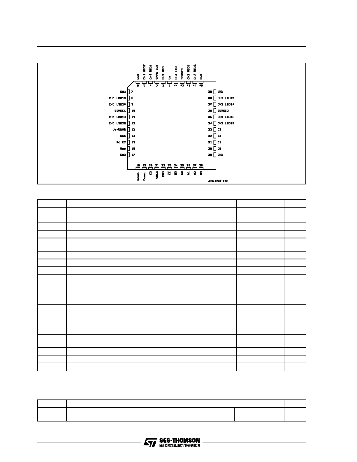
PIN CONNECTION (top view)
ABSOLUTE MAXIMUMRATINGS
Symbol Parameter Value Unit
V
V
SS
V13 Pin 13 InputVoltage (Note B) 60 V
V
DHS
V
V
OD
V
sense
V
I
LSD
I
HSD
I
SSOUT
I
RES
P
tot
T
stg;Tj
Notes: A) D0 =D1 = D2 = D3 =0; B) V13 = VS+V
D) D0 = 1; D1 = D2 = D3 = 0; E) D1 = 1; D0 =X; D2 =D3 = 0; F) The pulse width must be< 5ms and the Duty Cycle must be < 10%
G) The pulse widthmust be <5ms and the Duty Cyclemust be< 6%; H) mounted on board with minimized dissipatingcopper area.
THERMAL DATA
Power Supply Voltage (Note A) 35 V
S
Logic Supply Voltage 7 V
High Side Out Transistor Driving Voltage (NoteB,C) 18 V
Output Voltage. CH1; CH2: Unipolar Motor Drive (Note D)
O
CH3
60
60
Differential Output Voltage CH1; CH2; FullBridge Configuration (Note E) 60 V
Sensing Voltage -1 to 2 V
Logic Input Voltage -0.3to VSS+0.3 V
I
Low Side DriverInput Current
CH1; CH2 DC Operation
Peak (Note F)
CH3 DC Operation
Peak (Note G)
0.7
2
3
4.4
High Side Driver Onput Current
CH1; CH2 DC Operation
Peak (Note F)
CH3 DC Operation
Peak (Note G)
SMPS Output Current (Continuous)
(Peak; TON< 5ms)
1
2
3
4.4
1
2
Reset Output Open Drain Input Current 16 mA
Total Power Dissipation atTamb = 70°C (Note H) 1.6 W
Storage an Junction TemperatureRange -40 to 150 °C
; C) At 20V > V
DHS
> 17V the input current at pin 13 mustbe < 30mA;
DHS
V
V
A
A
A
A
A
A
A
A
A
A
Symbol Description Value Unit
R
th j-pins
R
th j-amb
(*) Mounted on board with minimized dissipating copper area.
Thermal Resistance Junction-pins
Thermal Resistance Junction-ambient (*)
Max.
Max.
12
50
2/26
°C/W
°C/W
Page 3

PIN DESCRIPTION
PINS NAME FUNCTIONS
1V
S
2 HSD 1 High Side CH 3 Power Output
3 SMPS OUT Output of Switchmode Power Supply
4 HSD 1 High Side CH 1 Power Output
5 HSD 2 High Side CH 1 Power Output
6, 7,17,29,
GND Common GroundedTerminal
39, 40
8 LSD 1A Low Side CH 1 Power Output
9 LSD 2A Low Side CH 1 Power Output
10 SENSE 1 A Resistor Rsense, connected to this pinallows loadcurrent control for CH 1
11 LSD 1B Low Side CH 1 Power Output
12 LSD 2B Low Side CH 1 Power Output
13 V
14 V
S+VDHS
SS
15 Comp. An RC series network allows the compensation of the SMPS regulation loop
16 RES OUT The reset opendrain output can be used to warnthe microprocessor about V
18 R
19 C
20 C
21 V
22 t
OSC
OSC
D
DLS
WD
23 CS Enable Input(active when low)
24 WR Write Input. WhenWR is low the data is loaded into the µP interface
25 A0 Operation Selection (see programming sequence).
26 A1 Operation Selection (see programming sequence).
27 A2 Channel Selection (see programming sequence).
28 A3 Channel Selection (see programming sequence).
30 D0 Data (see programming sequence).
31 D1 Data (see programming sequence).
32 D2 Data (see programming sequence).
33 D3 Data (see programming sequence).
34 LSD 2B Low Side CH 2 Power Output
35 LSD 1B Low Side CH 2 Power Output
36 SENSE 2 A Resistor R
37 LSD 2A Low Side CH 2 Power Output
38 LSD 1A Low Side CH 2 Power Output
41 HSD 2 High Side CH 2 Power Output
42 HSD 1 High Side CH 2 Power Output
43 SENSE 3 A Resistor R
44 LSD 1 Low Side CH 3 Power Output
Power Supply Voltage Input
Input Voltage for the HSD Gates Drive
Logic Supply Voltage Input
and VSSstatus
Together with C
Together with C
, sets the cycle time ofthe SMPS t = 1.1 ROC
OSC
, sets the cycle time ofthe SMPS t = 1.1 ROCOand sets the
OSC
minimum ON time in the PWM current control loop
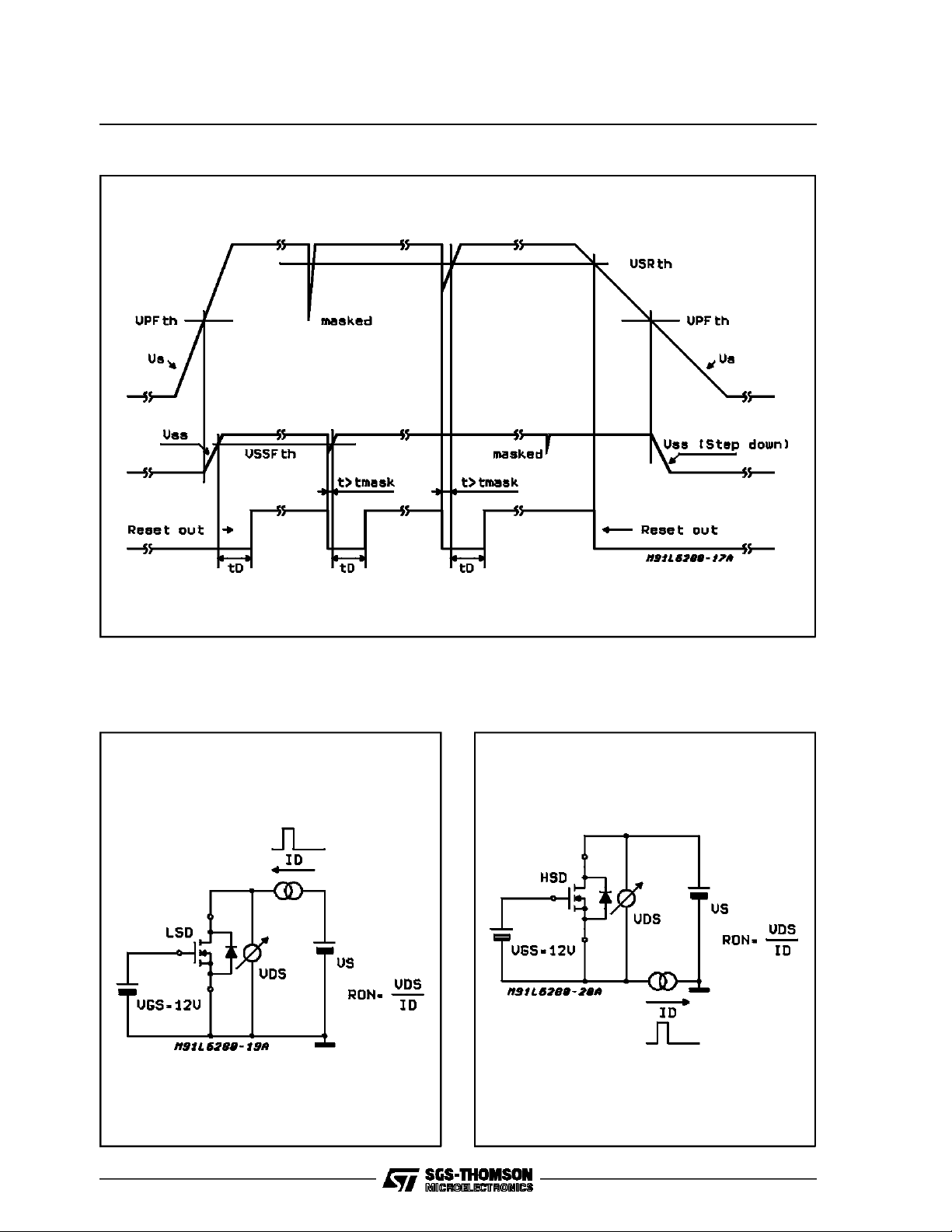
The value of this capacitor sets the reset delay tD=7 x10⁴C
D
By-pass Capacitorof the LSD Gates Voltage drive
ThevalueofthisCWDsetsthedurationofthewatchdogmonostable tWD=3x 10⁴CWD.
If no watchdog signal is generatedinto the TWD timethe device is automatically
switched off.
, connected to this pin allows load current control forCH 2
sense
, connected to this pin allows load current control forCH 3
sense
L6280
S
O
3/26
Page 4
L6280
ELECTRICALCHARACTERISTICS (VS= 20V; Tj=25°C; VSS =5V; V
C
=680pF; unlessotherwise specified)
O
=15V; RO=165KΩ;
DHS
Symbol Parameter Test Condition Min. Typ. Max. Unit
I
DSS
V
s
V
INL
I
INL
V
INH
I
INH
V
ROUT
V
PF
I
S
V
SS
I
SS(IN)
I
SS(OUT)
f
osc
f
1
f
1max
f
2
f
3
Leakage Current Fig. 1 VDS = 60V 2 mA
Power Supply Voltage Note 1,2 >V
PF
48 V
Low Level InputVoltage -0.3 1.35 V
Low Level InputCurrent -10 µA
High Level InputVoltage 3.15 VSS V
High Level Input Current 10 µA
Low Level Reset Out I16 = 1.5mA 0.8 V
Power Supply Fail Voltage (Fig. 2) 13 V
Quiescent Supply Current VS = 12V 4.5 6 7.5 mA
Logic Supply Voltage 4.75 5 5.25 V
Logic Supply Current 4.5 6 7.5 mA
SMPS Out Current Range Note 3 800 mA
Oscillator Frequency 64 80 96 KHz
SMPS and CH3 Frequency f
osc
Max SMPSSwitching Frequency 120 KHz
PWM Frequency fosc/2 KHz
High Side Driver Switching
fosc/4 KHz
Frequency
TSD Thermal Shutdown 125 150 °C
t
WD
t
D
R
ON
Monostable Watchdog Time CWD = 0.22µF (Note 4) 6.6 ms
Reset Delay Time CD= 0.22µF; Fig.2 (Note 5) 15.4 ms
ON State DrainResistance
Transistor LSD CH1 - CH2
HSD CH1 - CH2
LSD CH3
HSD CH3
SMPS
Fig 3; 4ab
2
1.1
0.5
0.5
1
2.4
1.4
0.8
0.8
1.2
SENSE Internal Sense LOW-Pass Filter 300 500 ns
V
ref
DAC Reference Voltage D0=D1=D2 =1 (Table 1) 1 V
DAC DAC Resolution (3 Bit) (See Table 1) Vref/8 V
t
C
Discarge Time of Cosc
(Note 6) 0.4 µs
Capacitor (Minimum TON)
V
DHS
I
DHS
I
SS (OUT) max
HSD Gates Voltage Drive 13 15 17 V
Pin 13 OverageInput Current 3 mA
SMPS Overload Protection
1.2 A
Current
V
DLS
V
SSF
V
FHSD (1;2)
Pin 21 OverageInput Voltage 12 V
Logic VSS FailThreshold Voltage (Fig. 2) 2.6 4.1 V
Internal Clamp Diode Forward
@IDS = 0.4A (Fig. 5) 1.2 V
Voltage CH1/CH2
V
FLSD
(1AB;2AB)
V
FHSD
Internal Clamp Diode Forward
Voltage CH1/CH2
Internal Clamp Diode Forward
@IDS = 0.4A (Fig. 5) 1.4 V
@IDS= 1A (Fig. 5) 1.1 V
Voltage CH3
KHz
Ω
Ω
Ω
Ω
Ω
4/26
Page 5

ELECTRICALCHARACTERISTICS (continued)
Symbol Parameter Test Condition Min. Typ. Max. Unit
V
FLSD
Internal Clamp Diode Forward
Volt. CH3
t
CW
t
WPW
t
SU
t
DH
t
WC
Notes:
1) When driving a unipolar stepper motor the Power Supply Voltage must be lower than24V.
2) A lower Supply Voltage than the Power Fail thresholddisables the Step Down Power Supply (see Fig.2)
3) The minimumoutput current equals the half of the peak-to-peak current ripple
4) t
WD ≅ CWD
5) t
x 3.5 /50 x 10
D ≅ CD
6) t
C≅ COSC
Chip Seletion to End of Write (Fig. 6) 700 ns
Write Pulse Width (Fig. 6) 700 ns
Data Set-up Time (Fig. 6) 700 ns
Data Hold-up Time (Fig. 6) 0 ns
Write Cycle Time (Fig. 6) 2.7 ms
x 1.5 /50 x 10
x R
(sec); R
int.
-6
(sec)
-6
(sec)
= 600Ω ± 30%
int.
@IDS= 1A (Fig. 5) 1.1 V
L6280
Figure1: DrainLekage Current Equivalent Test
Circuit. The Gate-to-Source Voltage
VGS is below theSwitch-Off
Threshold.
Figure3: TypicalNormalized R
JunctionTemperature
DS(ON)
vs.
5/26
Page 6
L6280
Figure2: Reset Output Behaviour versusPower Supply Voltage V
and/orLogic SupplyVoltage VSS.
S
Figure4a:Sink Output DMOSRONEquivalent
Test Circuit
Figure4b:Source OutputDMOS R
Test Circuit
Equivalent
ON
6/26
Page 7
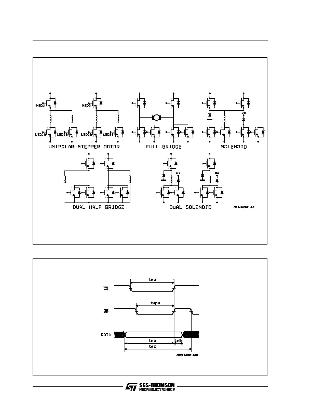
Figure5: Possible HardwareConfigurationsof PowerStage (CH1and CH2)
L6280
Figure6: Write Cycle
7/26
Page 8
L6280
SYSTEM DESCRIPTION (Refer to the Block Dia-
gram)
The L6280 is a single chip power microsystem
which includes drives for three differentloads, the
associated control logic and a Switched Mode
PowerSupply(SMPS) at V
=5V± 5%.
SS
The IC can be directly connected to a standard
microprocessor because of its common I/O interface architecture. The L6280 can exchange information regarding the load driver and the control
methodvia a 8 bit data bus. The blocknamed microprocessor interface decodes the first four bits
(A0....A3),which, depending on the content of the
remainingfour(D0.......D3)are used to enable the
power DMOS, to activate the PWM loop, and finally to set the D/A output value.
The power stage can be divided into 3 channels.
Channels1 and 2 have 6 DMOS transistors each
one (2high side drivers with R
drivers with R
=2Ω). Depending on the appli-
dson
=1Ω, 4 low side
dson
cation load, these driver transistors can be connected in different ways. The microprocessor, via
software, must activate the proper control loop to
optimize operation of different loads and output
stage configurations. Because of this programmability in the control of the output configurations,
a large variety of different loads can be driven by
the same integrated circuit (see possible configuration for power stage on Figure 5) giving the
greater system flexibility. Current levels up to 1A
are possible from CH1 and CH2, limited primarily
by the power dissipation of the IC.
The third channel has a fixed configuration intended to drive a solenoid. DMOS transistorswith
0.5Ω R
are used to provide 4A max load ca-
dson
pability.
All three channels have 3 bit current D/A resolution. Some auxiliary blocks of diagnostic and protection(e.g.: Thepower Fail/Reset andthe watchdog) are provided to protect the system from
microprocessorfailure or powerfail.
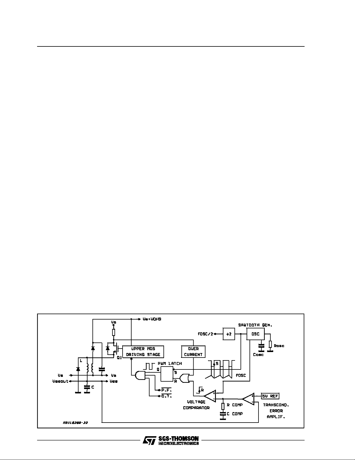
Figure7: SMPSBlock Diagram
Step Down Switchmode Power Supply (See
Figure7).
The step down switchmode power supply con-
tains a DMOS power stage with 1Ω R
dson
(Q1),
control circuitry, diagnostics and protection circuits; a regulated voltage (V
is used to drive
SSout)
some of the internal circuit blocks and the external microprocessor and memories. Thanks to the
DMOS output stage this regulator can deliver a
continuousoutput power of 4W (5V; 0.8A) with an
efficiency betler than 90% at a typical frequency
of80kHz.
The regulation loop uses a classical pulse width
modulation circuit that includes a sawtooth generator,an erroramplifier,a voltagecomparatoranda
PWM latch. A precision 5V referenceis generated
and trimmed on chip to guaranteea 5% tolerance.
This referenceis used as voltage referencefor the
SMPSand the reference for the DACs.
The IC also provides an extra voltage (V
S+VDHS
for the correct driving of the high side drivers.
These transistors require a gate voltage higher
than the supply voltageVs to obtainthe minimum
ON resistance. Because of the v ery low current
needed to drive DMOS transistors, this auxiliary
voltage is easily obtainedfrom a second winding
on the inductor of the LC output network (see ApplicationInformation).
An overcurrent protection circuit is included to
turn OFF the power transistor when a current
levelof 1.2A isexceeded.
The SMPS block also includes a voltage sensing
circuitto generate a powerON reset signal for the
microprocessor. This Power Fail circuit senses
the input supply voltage and the output regulated
voltage and sets the Reset-out pin to the high
voltage only when both the sensed voltages are
correct.
Finally, the SMPS block is able to deliver f
OSC/2
used in the actuation stage for the PWM control
of the current(CH1; CH2 and CH3).
)
8/26
Page 9

L6280
PwmCurrentControl Loop
The current control is achieved big a cycle of
charge (T
) and discharge (T
ON
) of the energy
OFF
stored in each couple of windings of the driven
motor (MA and MB). Fig. 8 shows the windings
MA of an unipolar stepper motor during T
ON
. FF1
is setted by the clock pulse and the transistor Q
is ON. At the moment Q1is ON the current exponentiallyincreases until R
A reset pulse is produced, Q
and Q
netic flux 0
is switched ON (Fig. 9). Since the mag-
2
=NAIPcannot suddenly change
MA
IPequalsV
x
S
A
.
REF
is switched OFF
and since the coil tourus number in the discharge
loop is doubled, the peak current I
self into I
/2. The OFF time is characteryzedby a
P
slow recirculation of the current I
creases until a new clock pulse sets a new T
modifies it
P
/2 that de-
P
ON
configuration. To control the current in two separate windings MA and MB with just one sense resistor RS and one comparator, a special PWM
control loop based on a ”time sharing” technique
(Patented)is used(Fig. 10).
In this configuration the chopping frequency, that
defines the T
ON+TOFF
period of each phase, is
halved by FF3 that drives ON G1 and G2 alternately. During T
MA (and Q
A
of one winding, for instance
OFF
is OFF), its current does not flow
throught the sensing resistor that can be used to
monitor the current that flows through the second
windingMB, allowed by the ON-statusof Q
.
B
Fig. 11 shows a simplified timing before and during the phase change from AB to AB (CCW, full
step). It can be seen that before the time t
and IBare alternatelycontrolled in a choppingperiod Tch1 of 4 oscillatorperiods or two clock periods. The time sharing is 50% - 50% and the
chopping frequency is typically of 20KHz (f
80KHz).
Afther the time t
A
ferent time sharing is generated. In fact since a
, as soon as IAis sensed, a dif-
1
Reset pulse is last after one clock pulse, FF2 can
drive FF3 to change for I
chopping only at the
B
next clock pulse (Fig 10; Fig 11).
Thismeans that the choppingtime becomesTch2
= 6 oscillator pulses, the frequency decreases to
16.6KHz (f
= 80 KHz) and the time sharing be-
osc
comesof67% - 33%.
At the end of the phase change period tphc the
time sharing comes back to 50% - 50% again. It
can be noted that this behaviour allows a faster
phase change and then a higher speed of the
motor. The cost of that, is the increase of the
of the unchangedphase B and then a small
T
OFF
increase of the ripple of the current I
<∆IB2in Fig. 11).
This time sharing current control method is also
used when two indipendent load are driven by
one single channel. when only one load is present,such as a DCmotor could be, the timesharing is automatically switched OFF and the PWM
frequency becomes f
/4 = 20KHz. Table 1
osc
showshow the referencevoltage can be modified
with a three bits DAC to allow microstepping operations(see below).
(see ∆I
B
1,IA
osc
=
B1
Figure8 - T
Configuration:Motor Windings
ON
MA (A;A).
Figure9 - T
Configuration:Motor Windings
OFF
MA (A:A).
9/26
Page 10

L6280
Figure10 - PWM CurrentControl Loop. Time Sharing Technique.
Figure11: Chopping Characteristics(simplified)
10/26
Page 11

L6280
Digital/AnalogConverters(DACs)
The output current levels are programmed by
5DACseach with 3 bit resolution. Channels1 and
2 each have 2 DACs, one for the left part of the
output stage and the other for the right part.
When the output stage is used to drive only one
load (as with DC motors), the L6280 uses only
the right register. Channel3 has only 1DAC.
Microstepping operation is easily performed with
channels1 and 2. The value of each DAC can be
changedin two ways:
a) the new value can be directly generated by
the microprocessor and then loaded into the
specifiedDAC;
b) the value of a DAC can be incremented or
decrementedby 1; in this case the microprocessor during acceleration or deceleration has
only to indicate the DAC on which operate
and the type of the operation, reducing the
CPU’sburden.
The correspondence between the DAC value and
the Vref level is shown in table 1.
Table 1
D2 D1 D0 V
1111 V
1 1 0 0.875 V
1 0 1 0.75 V
1 0 0 0.625 V
0 1 1 0.5 V
0 1 0 0.375 V
0 0 1 0.25 V
0 0 0 0.125 V
ref
UNIT
Iload = 0 is obtained bydisabling all low-sidedrivers.
Turn ON/OFF Characteristicsand Program Sequence
During power-on the Switchmode Power Supply
output stage is turned OFF till V
reaches V
S
PFth
The pin Reset Out is held low and remains low till
is < V
V
SS
(the powerstages and the logic of
SSFth
the L6280 aredisabled.
Not correct signals coming from the microproces-
sor are then ignored; the microprocessor on the
other hand, receives a low state signal from the
Reset Out pin. When the V
during a delay t
set by the CDcapacitor, the pin
D
output is stabilized
SS
Reset Out goes to the high level; the microprocessor is enabled to work while the L6280 is in
stand-by waiting for a keyword and initialization
sequence.Every command that arrives beforethe
keyword is ignored. At this time the programming
sequence can start accordingto the flow diagram
(Fig.12).
At first the Keyword (00111010) has to be sent to
the L6280 to activate the watch - dog function
that begins to control the microprocessor functionality. From this moment the microprocessor
must send periodically the Watch-dog word
(00110101) otherwise its absence is interpreted
as a microprocessor failure: to prevent any damage both in the load and in the IC, the L6280itself
disablesthe power stages. No reset signal is generated towards the CPU; the system must restart
the sequencefrom Power-ON.
The next step is to set the configuration of channel 1 and channel 2 output stages by the initialization word. The configuration can be chosen to
fit in the load characteristics.To do thisthe microprocessor generates a word with A0, A1 = 0 and
where A2, A3 choose the channel to be configured, D0 to D3 choose the type of configuration
(unipolar, dual half bridge or full bridge; see Data
and Address decoding). Every input configuration
different from the allowed initialization word is ignored.
Whenthe initializationarrives, the L6280 sets the
configuration of the output stage of the chosen
channel. The initialization word has to be repeated for the other channel (CH1 or CH2 only). If
two initializations arrive for the same channel,the
L6280 disables the output stages while pin Reset
Out goes low for a time Td to advise the mocroprocessorabout the uncorrectcondition.The program sequence must restart from the Keyword
step. After the initialization step is succesfully
completed the L6280 begins to accept commands. If a command is sent before the relative
channel has been configured, the command is
neglected.
Commandcan be of three type:
a - selectionof currentlevel loading a DAC;
b - increment or decrement of aDAC;
c - selection of the driving strategy of a channel
(e.g. half/fullstep, fast/slowdecay and so on).
To select the current level is necessary to load a
value into the appropriateDAC. The microprocessor must select the channel via A2, A3 and (only
for channel 1 and2) left or right DAC via D3; the
.
value of D0,....D2 are loaded in the chosen DAC.
There are two possibilities of changing the value
of a DAC; the first one is to load directly the new
value,the second one is to causean incrementor
a decrement in a DAC, in this way the burden of
the microprocessor can be partially decreased
generating inc/dec command without calculating
the value.
To incrementod decrement a DACthe microprocessor must select the channel via A2,A3, left or
right DAC and the operationvia D0 to D3 according to truth table in Datas and Address Decoding
(see below). The increment or decrement is done
immediately after the arrive of the command. For
every configuration of the output stages are possible different type of driving strategy explained in
Datasand Address Decoding.
11/26
Page 12

L6280
Figure12: ProgramSequence
Dataand Address Decoding
SPECIALWORDS
A3 A2 A1 A0 D3 D2 D1 D0
00111010
KEYWORD
This word is used during the start-up procedure to
enable operations; all settings arrived before the
keywordare reset.
A3 A2 A1 A0 D3 D2 D1 D0
00110101
WATCHDOG
The microprocessor must periodically generate
this word; the value of the maximum period is set
by the capacitor C
. The absence of the Watch-
D
dog is interpreted by L6280 as a microprocessor
failure.The maximumperiodis:
T
WD=CD
1.5 / ( 50 x 10E-6)
x
Except for special words (keyword and watchdog), the input words are organized like the following:
A0 A1 Operation selection
A2 A3 Channel selection
D0 D1 D2 D3 Datas
A0,A1DECODING(OPERATIONSELECTION)
A0,A1selectthe type ofoperation (channel initiali-
zation,commands, DACs loading, DAC increment/decrement).
A0A1
0 0 This configurationis usedto send the infor-
mationabout the configurationof the
vchannelspecifiedby A3 and A2; D0 to D3
are used to specify the configuration of the
channel(full bridge, dual half bridge,unipolar motor).
A0A1
1 0 This configuration is usedto changedriv-
ing strategyof the output stagesof the
channelspecifiedby A3 and A2 (full/half
step, slow/fastdecay and so on). The driving strategyis codedin D0 to D3, and dependsfrom the configurationof the output
stage.
A0A1
0 1 This configurationis usedto load the value
of a DAC of the channel selected by A3
and A2. D3indicates rightand left DAC
just for channel1 and 2.
12/26
Page 13

L6280
A0 A1
1 1 Thisconfigurationis used to cause an incre-
ment or a decrement of a DAC. Right or
left DAC and inc/dec are selected by
D0 toD3 value.
D0 to D3 DECODING(Datas)
The meaning of D0, D3 changes according to
the value of A0, A1
A0A1
0 0 When A0,A1 are in this configuration,and
A2, A3 DECODING (Channel Selection)
Every time a command or a initializationis sent to
the L6280, a channel must be selected. This is
done via A2 and A3 accordingto the table.
A2 A3
0 1 Select channel 2
1 0 Select channel 1
1 1 Select channel 3
0 0 Used only with keyword and watchdog
D3 D2 D1 D0
0 0 0 0 Null (power disabled)
a 0 0 0 1 Unipolarmotor
b 0 0 1 0 Full Bridge
c 0 0 1 1 Dual Half Bridge
b) Full Bridge Configuration
a) Unipolar Motor Configuration
In this configurationD0 to D3 directlydrive the low side drives:
D3 D2 D1 D0
0000
0001
0010
0100
0101
0110
1000
1001
1010
Low side drivers 1,2,3,4 OFF
Low side drivers 2,3,4 OFF Low side driver 1 ON
Low side drivers 1,3,4 OFF Low side driver 2 ON
Low side drivers 1,2,4 OFF Low side driver 3 ON
Low side drivers 2,4 OFF Low side drivers 1,3 ON
Low side drivers 1,4 OFF Low side drivers 2,3 ON
Low side drivers 1,2,3 OFF Low side driver 4 ON
Low side drivers 2,3 OFF Low side drivers 1,4 ON
Low side drivers 1,3 OFF Low side driver 2,4 ON
Configurations
channel1 or 2 is selected, the data appearing in D0 to D3 set the outputpower stage
configurationto fit the chosedload according to the allowed Truth Table. There is no
need to configure channel 3.
Possible configurations for
channels 1 and2
The following configurations are not allowed: the microprocessor does not to generate them otherwise
they can cause faulty operations.
D3 D2 D1 D0
0011
0111
1011
1100
1101
1110
1111
Alwaysnot allowed
This configurationis not allowed when drivinga unipolar motorand it is
permittedonly to drive a high currentsolenoid.
13/26
Page 14

L6280
In full bridge configuration D0 to D3 set the driving strategy of the bridge:
D0 D1 D2 D3
X 0 0 0 Tristate leftand right
X 0 0 1 Chopper left, brake right
X 0 1 0 Chopper right, brake left
X 0 1 1 Brake left, brake right
X 1 0 0 Tristate leftand right
X 1 0 1 Diagonalchopper
X 1 1 0 Inverted diagonal chopper
X 1 1 1 Tristate leftand right
c) Dual Half Bridge Configuration
D0 D1 D2 D3
X 0 0 0 Tristate leftand right
X 0 0 1 Brake right, chopper left
X 0 1 0 Brake right, chopper right
X 0 1 1 Brake left, brake right
X 1 0 0 Chopper left, chopper right
X 1 0 1 Tristate left, chopper right
X 1 1 0 Tristate right, chopper left
X 1 1 1 Tristate leftand right
CHANNEL 3
For channel 3 only D0 has a meaning: it directly
drives the low side driver DMOS. When D0 = 0
the low side driver DMOS is switched OFF and
the current flows through external recirculation diodes.
(only for channel 1 and 2)
D3
0 LeftchannelDAC
1 Rightchannel DAC
For channel 3, D0 to D2 are loaded into the
uniqueDAC.
A1A0
1 1 WhenA0, A1 are in this configuration, the
value of D0 to D3 causesan incrementor
a decrement of the content of left/right
DACof a channel. The inc/dec operation
and the DAC register selection(rightor
left) are selectedaccording to the following
truth table:
D3 D2 D1 D0
dec LEFT inc LEFT dec RIGHT inc RIGHT
The change in DAC registersis done immediately
after receiving the data.The configurationsD3, D2
= 11 and D1, D0 =11 are not allowed. (Them can
cause faulty operations) Channel 3 has only one
DAC; the change in its value is doneaccording to
D0,D1value.
D1 D0
dec DAC inc DAC
D1, D0 = 11 is not allowed (they can cause faulty
operations).
OutputOperation
In full bridge and dual half bridge configurations,
the output stages will operate according to D1,
D2,D3 values.
A0 A1
1 0 When A0, A1 are in this configuration,D0
to D3are used to set the strategyof the
output power stages according to the output stageconfiguration previouslyselected.
A1 A0
1 0 When A0, A1 are in this configuration,
D0 toD2 are loaded into left or rightwinding D/A converter,accordingto D3 value
14/26
FULL BRIDGE CONFIGURATION (CH1 and
CH2)
In full bridge configuration the cennection between the output of the high side drivers and the
corresponding low side drivers has to be made
with external jumpers. The output stage diagram
here below (Fig. 13) must be substituted inside
the blank boxes in the following block diagrams.
Page 15

L6280
Figure13
D0 D1 D2 D3
X 0 0 0 Tristate left and right
All output DMOSs of the channel are OFF (Fig.
14)
Figure14
Figure15
D0 D1 D2 D3
X010
hopper right side, fixed
left side (one phase
chopping)
As above but with the two channel exchanged
each to other(Fig. 16).
Figure16
D0 D1 D2 D3
X001
Chopper left side; fixed
right side (one phase
chopping)
The left side of the bridge is controlled by the
PWM loop while HSD2 is held OFF and LSD2A
and 2B are held ON. During ON time (Q low) the
current flows thrugh HSD1, motor winding and
LSD2A and 2B. During OFF time the current can
recirculate through LSD1A, 1B, 2A and 2B (Fig.
15)
D0 D1 D2 D3
X011
Fixed both leftand right
(brake action)
All High side drivers are held OFF while all low
side drivers are held ON. The motor winding is
short circuited through the low side drivers; the
motor’s back EMF acts as a brake voltage (Fig.
17).
15/26
Page 16

L6280
Figure17
D0 D1 D2 D3
X100
D0 D1 D2 D3 INVERTED DIAGONAL CHOPPER
(Twophase chopping)
During ON time (Q = LOW) the current flows
through HSD2, motor winding and LSD1A and
1B. During OFF time (Q = HIGH) the current can
recirculate through LSD2A and 2B motor windind
and HSD1 (Fig.19).
Figure19
Three state left and right
(see X000 configuration)
D0 D1 D2 D3
X101
Diagonal chopper (Two
phase chopping)
During
During On time (Q=LOW) the current flows
through HSD1, motor winding and LSD2A and
2B. During OFF time (Q = HIGH) the current can
recirculate through LSD1A and 1B motor winding
and HSD2 (Fig. 18).
Figure18
D0 D1 D2 D3
X111
Tristate left and right (see X000
configuration)
16/26
Page 17

L6280
DUAL HALF BRIDGE CONFIGURATION (CH1
and CH2)
In dual half bridge configuration the connection
between the output of the high side drivers and
the corresponding low side drivers has to be
made with external jumpers. The output stage
block diagram shown in figure 20 must be substituted in side the blank boxes in the following
block diagrams. In dual half bridge configuration,
the time sharingstrategy is always used.
Figure20
Figure21
D0 D1 D2 D3
X 1 0 1 Tristate left, chopper right
During ON time (Q = LOW) the current flows
through high side driver HSD2, right winding and
sense resistor. During OFF time the current recirculate through winding and side drivers LSD2A
and LSD2B (Fig. 22).
D0 D1 D2 D3
X 0 0 0 Tristate leftand right
X 0 0 1 Chopper left, fixed righ
X 0 1 0 Chopper right, fixedleft
Fixed left and right. For these
X011
D0 D1 D2 D3
X 1 0 0 Chopper left chopper right
configurations, see the
corresponding shown in Full
Bridge Configuration paragraph
(Page 14/24).
As foreseen when in unipolar motor configuration(see Figure 5), the time sharing strategy is
used (see Figure 10), so when the current in left
winding is controlled, the current in right winding
recirculate trough the low side drivers and not
throughthe sense resistor(Fig. 21).
Figure22
D0 D1 D2 D3
X 1 1 0 Tristateright, chopper left
During ON time (Q = LOW) the current flows
through high side driver HSD1, left winding and
sense resistor. During OFF time the current recirculate through the winding and low side drivers
LSD1Aand LSD2A(Fig 23).
17/26
Page 18

L6280
Figure23
D0 D1 D2 D3
X111
Tristate left and right (see
X000 configuration of full
bridge).
APPLICATIONINFORMATION
An application circuit useful to test the performance of the L6280 can be formed as shown on
Figure 24: CH1 drives one unipolar stepper motor, CH2 drives a DC motor, CH3 drivesone solenoid and theSMPS can supply continuously0.5A.
If the Watch Dog and the Chip Select functions
are not of interest, pins 22 and 23 must be
grounded. Each sensing resistor would be obtained by the parallelof two or more metal film resistor of the same value to minimize their series
equivalentinductance.
Generally, optimum stability of the SMPS voltage
control loop, is achieved by a series network
made by 1nF and 39 KΩ (seepin 15) and by using an output capacitor of 100µF having an
equivalent series resistance of 100 mΩ (see pin
14):the mostofthe unexpensivealuminium electrolithiccapacitors can be right.
The snubber network at the secondary windingof
the step-down inductor can be saved by accepting a not regulated voltage at the Charge Pump
input pin 13. This condition is not recommended
when the supply voltage and/or the SMPS output
current changes too much (for instance respectively20V + 30%and/or 100 to 800 mA).
Theinductance value of the primary winding of T1
defines the peak-to peak current ripple that flows
throught itself, that is the minimum output current
that allows the correct behaviour in continuous
mode of the SMPS; nevertheless, the device is
not demaged if it is obliged to work in discontinuousmode at a low current level.
Figure 25 shows the characteristics of the transformer T1 suitable to be used on the Application
of Figure 24:
The maximum output current is of 500 mA continuous but current peaks of 800 mA can be
sinked out without the risk of the core saturation.
To avoid the discontinuous mode, the minimum
SMPSoutput current must be of 70mA. The rectified voltage trend for the high side gate drive at
pin 13 is as shown on Figure26.
Not equally cheap, the choice of a toroidal core
for T1 canoptimize theapplication.
Instead of this, another solution can be as in Figure 27a it is shown. This is a full wave rectifier of
the voltage at pin 3; Z1and R1 clamp the positive
peak while the forward characteristicof the Zener
rectifies the negative peak and charges C1. The
recommendedZener voltage is of 12V.
Could happen that the V
output voltage is not
SS
requestedbecause already available:in this case
and only if at least one unipolar stepper motor is
continuously driven, the solution shown in Figure
27b can be implemented. The step down output
componentscan be left out.
Theconnectionof the network is as follows:
A: to pin 4 (or pin 5) when the unipolar motor is
drivenvia CH1;
to pin 41 (or pin 42) when the unipolar motor
is drivenvia CH2;
B: to pin 1
C: topin13
TheSMPS switching frequency is the sameof the
oscillator frequency that can be typically defined
by:
f
osc
Referringto Fig. 24 it iscalculated f
9
=
RC
= 82KHz.
osc
CH3 is chopped at the same frequency. The output diodes must be chosen according to the solenoid working current (50ns of reverse recovery
time or better): for a current less than 1 A, the
PLQ08is a goodchoice.
Drivingone unipolar stepper motor, output protection diodes (Transil) are recommended: CH1 in
Fig 24 uses four BZW04 - 48 diodes; when a low
current motor is driven or a Vs less than 20V is
supplied, four fast diodes and only one Zener diode can be used as a protection of the outpus
(see Figure 28). The driving of DC motor needs
the connection as shown for CH2 (full bridge configuration).
The drive of one bipolar stepper motor by using
CH1 and CH2 both in full bridge configurationallows the use of a higher supply voltage level that
however cannot exceed the Absolute Maximum
18/26
Page 19

L6280
Ratings of 35V:a max value of 33V is reccommended.
In this case, at each couple of outputs for the bipolar windings, a snubber network must be connected. This network is doneby the series of a resistorand of onecapacitor:
R
snub=VS
C
snub
max/Imotorpeak;
= Imotor peak/ (dv/dt)
One dv/dt of 200V/µsec is generally a correct
choice.
Of course, care must be taken in the Printed Circuit Board design regarding the ground paths and
Figure24: ApplicationTest Circuitof the L6280
the high current loops.
An example of P.C.B. layout is shown in Figure
29ab; Figure 30 shows the SchematicDiagram of
the circuit of the L6280 S.P.D. S.AB.
The driving signals useful for this board can be
easily generated by using an additional board
(EMUKIT 512) not describedhere.
On Figure 29a itcan be observedthe copper area
near the I.C. is used to sink out the heat from the
device. Useful thermal characteristics of the
L6280are shown in Figure 31 and 32.
19/26
Page 20

L6280
Figure25: Characteristicsof the TransformerT1.
N1: 118 tourns, copperwire ∅ 0.35mm
N2: 88 tourns, copperwire ∅ 0.2mm
TYPICALPARAMETERS
L
= 560µH
N1
N2
1
= 680mΩ
R
1
= 300µH
L
2
= 1.5Ω
R
2
@ 1KHz
@ 1KHz
Figure26: Charge Pump Voltage vs. Supply Voltageby using the transformershown on Figure25
20/26
Page 21

Figure27a : OtherCharge PumpSolution Figure 27b : OtherChargePump Solution
Figure28 : Unexpensive Output Protection Net-
work for theUnipolar MotorDriving
L6280
21/26
Page 22

L6280
Figure29a: L6280 PCB Components Side (1st metallization)
22/26
Page 23

Figure29b: P.C.B. Back Side (2nd metallization)
L6280
Figure30: SchematicDiagram of the CircuitAssembledon the L6280-AB(Figure 29)
23/26
Page 24

L6280
Figure31; TypicalTransientThermal Resistance
vs. Single Pulse Width.
Figure32; Typical ThermalResistance vs.
HeatsinkingCopper Area.
24/26
Page 25

PLCC44PACKAGE MECHANICAL DATA
L6280
DIM.
MIN. TYP. MAX. MIN. TYP. MAX.
A 17.4 17.65 0.685 0.695
B 16.51 16.65 0.650 0.656
C 3.65 3.7 0.144 0.146
D 4.2 4.57 0.165 0.180
d1 2.59 2.74 0.102 0.108
d2 0.68 0.027
E 14.99 16 0.590 0.630
e 1.27 0.050
e3 12.7 0.500
F 0.46 0.018
F1 0.71 0.028
G 0.101 0.004
M 1.16 0.046
M1 1.14 0.045
mm inch
25/26
Page 26

L6280
Information furnished is believed to be accurateand reliable. However,SGS-THOMSON Microelectronics assumes no responsibilityfor the
consequences of use of such information nor for any infringement ofpatents or other rightsof third parties which may result from its use. No
license is granted by implication or otherwise under any patent or patent rights of SGS-THOMSON Microelectronics. Specifications mentioned in this publication are subject to change without notice. This publication supersedes and replaces all information previously supplied.
SGS-THOMSON Microelectronics products are not authorized for use as critical components in lifesupport devices or systems without express writtenapproval of SGS-THOMSON Microelectronics.
1994 SGS-THOMSON Microelectronics - All Rights Reserved
SGS-THOMSON Microelectronics GROUP OF COMPANIES
Australia - Brazil- France -Germany - Hong Kong - Italy - Japan - Korea -Malaysia - Malta - Morocco - The Netherlands - Singapore -
Spain - Sweden - Switzerland - Taiwan - Thaliand - United Kingdom - U.S.A.
26/26
 Loading...