

Page 1
L6223
DMOS PROGRAMMABLE
HIGH SPEED UNIPOLAR STEPPER MOTOR DRIVER
HIGH EFFICIENCY UNIPOLAR STEPPER
MOTORDRIVER
HIGH SPEED UNIPOLAR STEPPER MOTOR
DRIVER
SUPPLYVOLTAGE UP TO 46V
PHASECURRENT UP TO 1A
UP TO 2A/PHASE IN DUAL CONFIGURA-
TION
PARALLEL CMOSµP INTERFACE FOR
FULL/HALFSTEP MOTOR ROTATION
SERIAL INTERFACE FOR 6 BIT PROGRAM-
MING
CLOSE/OPEN LOOP, 8 PWM CURRENT
LEVELS
DUAL PWM FREQUENCYSELECTION
INPUTBIDIRECTIONALLYPROTECTED
THERMALSHUTDOWN
DESCRIPTION
The L6223 is a programmable integrated system
for driving a unipolar stepper motor. It is realized
in Multipower BCD technology. The DMOS output
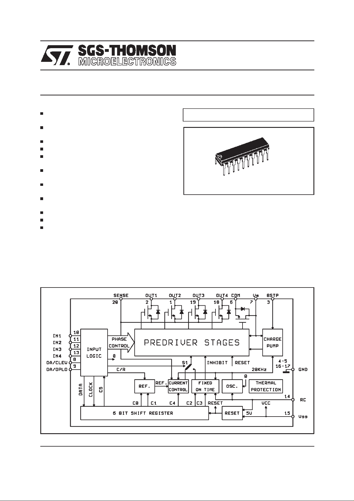
BLOCKDIAGRAM
MULTIPOWER BCD TECHNOLOGY
POWERDIP
16+2+2
ORDERING NUMBER : L6223
stage, realized by a single upper DMOS switch
and four lower DMOS,can deliverup to 1A/phase
with motor supplyvoltages up to 46V.
All inputsare CMOS and microprocessor compatible. An internal 6-bit shift register allows the device to be programmed to select different duty cycles in open loop mode and different chopping
frequencies in closed loop mode. When the current control is in closed loop mode it is also possible to select a reduced current chopping level to
optimize system efficiency. The L6223 is de-
March 1998
1/33
Page 2
L6223
signed to work with a single sense resistor. During chopping t(OFF) time the current is reduced
by half, improving efficiency.Higher current appli-
The L6223 is mounted in a 20-lead Powerdip
package, (16+2+2). Four ground leads conduct
heat to dedicated heatsinkarea on the PCB.
cations can be achieved by paralleling two L6223.
ABSOLUTEMAXIMUM RATINGS
Symbol Parameter Value Unit
V
SS
V
S
V
I
V
O
V
Opeak
I
pl
I
ph
P
tot
V
sense
T
stg,Tj
( * ) Oscillator running
(**)4cm
2
copper area on PCB, see fig. 34
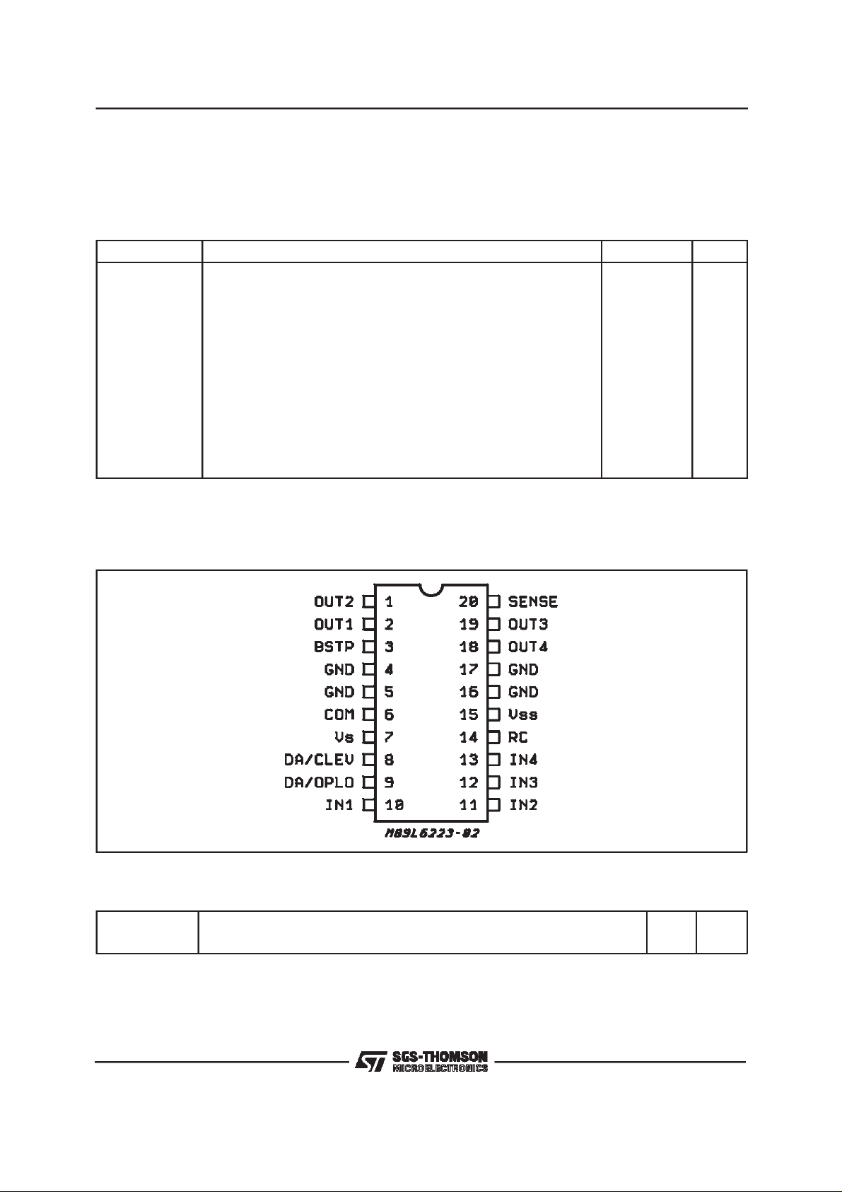
PIN CONNECTION
Logic supply 7 V
Supply voltage 50 V
Logic input voltage (*) – 0.3V to V
Output voltage 100 V
Output peak voltage (tpk = 5µs,10% d.c.) 125 V
Output sink peak current d.c. 10% t(on) = 10µs3A
Output source peak current d.c. 10%,t(on) = 10µs6A
Total power dissipation: T
=90°C 4.3 W
pins
=70°C (**) 2 W
T
amb
Sensing voltage – 1V to V
Storage and junction temperature – 40 to 150 °C
( topwiew )
SS
SS
THERMAL DATA
R
thj-pins
R
thj-amb
2/33
Thermal Resistance Junction-pins Max 14 °C/W
Thermal Resistance Junction-ambient Max 60
C/W
°
Page 3

PIN DESCRIPTION
No. Name Function
L6223
1,2
18,19
OUT2,OUT1
OUT4,OUT3
Outputs for motor windings.
3 BSTP A bootstrap capacitor connected between this pin and COM will
generate the internal overvoltage required for driving the gate of the
upper DMOS.
6 COM Output for common wire of motor.
4,5
GND Common ground. Also provides heatsinking to PCB.
16,17
7V
S
Power supply
8 DA/CLEV Digital input.
1) In PROGRAM MODE,operates in XOR withDA/OPLO to load data
into 6-bit shift register.
2) In OPERATING MODE,works with the otherdigital inputs to reduce
the current level (see Table 2 and Table 3).
9 DA/OPLO Digital input.
1) In PROGRAM MODE, operates in XOR with DA/CLEV to load data
into 6-bit shift register.
2) In OPERATING MODE,selects current control method: open loop(H)
or closed loop (L).
10,11
12,13
IN1,IN2
IN3,IN4
Digital inputs. When all inputs are low level,the device is in
PROGRAMMING MODE.
In OPERATING MODE:
1) FULLMODE - IN1 to IN4 drive the motor phases.
A previous programming is requested.
2) SIMPLIFIEDMODE - IN1 and IN2 drive the phases,IN3 is
ENABLE, IN4 works with DA/CLEV to enable the reduce current
level. Previous programming not needed.
14 RC Input for external RC network. Defines the higher of two possible
chopping frequencies. If this pin is set to ground it will reset the IC.
15 V
SS
Logic supply.
20 SENSE Output for sense resistor.
3/33
Page 4

L6223
ELECTRICAL CHARACTERISTICS (Tj=25°C, VS= 42V,VSS=5V, externalRC network: R =18kΩ,
C = 3.3nF,unlessotherwise specified).
Symbol Parameter Test conditions Min Typ Max Unit
V
S
V
SS
I
S
Power Supply 9 32 46 V
Logic Supply 4.5 5 5.5 V
Power Supply Quiescent
Current
I
SS
Logic Supply Quiescent
Current
I
OL
V
rs
Output Leakage Curr. VO= 100V (Fig. 1) 1 mA
Reset Threshold
Voltage (Pin 14)
T
BOOT
Bootstrap Refresh Pulse C
SINK MOS
R
DS(ON)
ON Resistance (Fig. 2a and Fig. 3) 1.2 Ω
SOURCEMOS
R
DS(ON)
ON Resistance (Fig. 2b and Fig. 3) 0.7 Ω
CURRENT CONTROL SECTION
IN1, IN2, IN3, IN4 = L
24mA
RC = 0V DA/CLEV = L
DA/OPLO = L
IN1, IN2, IN3, IN4 = L
14 20 mA
RC = 0V DA/CLEV = L
DA/OPLO = L
= 10nF 3 5 µs
BOOT
0.9 V
V
ref
f
(OSC)
t
(dis)
R
int
T
W
LOGICLEVELS
V
(IN)L
V
(IN)H
4/33
Internal Reference Volt. DA/CLEV = L; IN4 = H
I
= 100% nominal value
O
0.475 0.5 0.525 V
Oscillator Frequency (Fig. 20) 18 20 22 KHz
RC Network Discharge
Time (t
ON
min)
Internal Discharge Resistor
(Fig. 20) 2.3 3 4.3 µs
1.2 k
Ω
(pin 14)
Sense Filter Time Constant (Fig. 4) 1 1.4 2.3 µs
Input Low Voltage –0.3 0.8 V
Input High Voltage 2.4 V
SS
V
Page 5
ELECTRICAL CHARACTERISTICS (Continued)
Symbol Parameter Test conditions Min Typ Max Unit
SWITCHINGTIMING
L6223
t2, t4 Fall/Rise Time (IN1, 2, 3, 4) R
t1, t3 Input-Output Delay
t
dPWM
(IN1, 2, 3, 4)
Close Loop PWM
Control Delay
=39Ω(Fig. 5)
(load)
Pure Resistive Load to V
R
=39Ω(Fig. 5)
(load)
Pure Resistive Load to V
(Fig. 4) Note 1 1 µs
S
S
250 ns
700 ns
PROGRAMMING TIMING
t1 Loading Time (Fig. 6) 1.7 µs
t2 Protection Time (Fig. 6) Note 2 0.2 µs
t3 Data Set-up (Fig. 6) 0 ns
t4 Data Hold (Fig. 6) 1.6
t5 Setting Time (Fig. 6) 200 ns
Note 1) Upper DMOS turn ON delay when the signal is applied at the input comparator (point A in Fig. 4).
Note 2) Internal clock pulse isgenerated only if IN1...IN4 stay Low for almost 0.2 µs. This delay avoids undesirable programmings.
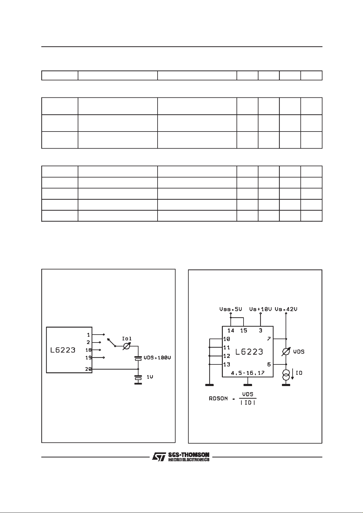
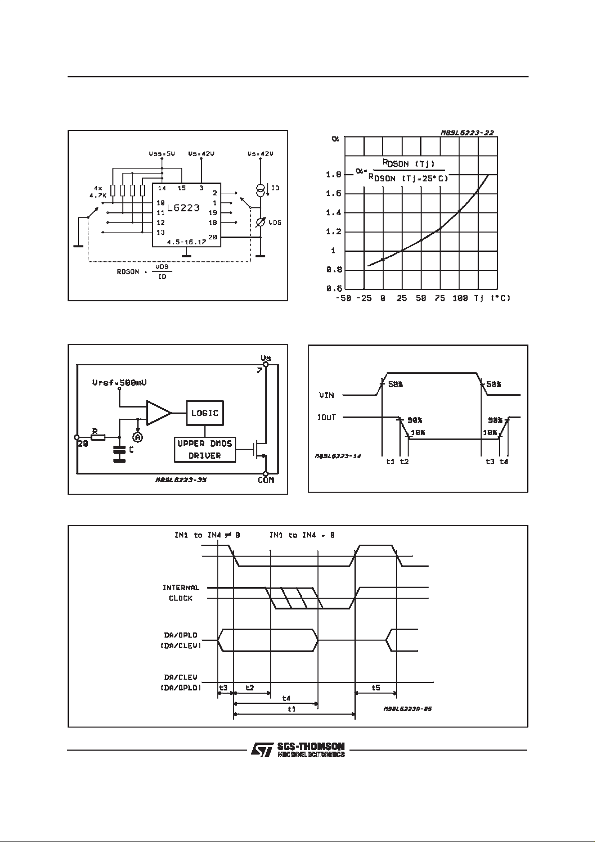
Figure1:
Outputleakage I
Test Circuit
OL
Figure2a:
Source Output DMOS R
DS(ON)
Circuit
µ
Test
s
5/33
Page 6
L6223
Figure2b:
Figure4:
SinkOutput DMOSR
DS(ON)
Test Circuit
SenseFilterRCTimeConstantandPWM
ClosedLoop control Circuit
Figure3:
Figure5:
Typical normalized R
DS(ON)
vs. Junction
temperature
OutputSink Current Delay vs Input
Control
Figure6:
6/33
ProgrammingTiming Diagram(see Block Diagram)
Page 7

L6223
BLOCKDIAGRAM DESCRIPTION
InputLogic
Decodes the input signals IN1, IN2, IN3, IN4,
DA/OPLO, and DA/CLEV for programming the
device and driving the motor. The six inputs are
CMOS compatible and can interface directly with
a microprocessor.
PredriverStages
Drive the gates of the five DMOS. They interface
the power section with the logic section. The internal inhibit, when activated, disables the power
section. The reset initializes the shift register and
disables the power section.
6 bit Shift Register
Internal memory which defines the working configuration of the device along with the input signals.
Current Control
When selected with the input DA/OPLO = L
(Closed Loop), it will maintain a constant output
current level by chopping. The value of the reference voltage, which is compared to the sense
voltage, is given by the Ref Block. The chopping
frequencydepends on bit C4.
Ref Block
Defines the current chopping level according to
bits C0 and C1 and the inputsignals.
Fixed on Time
When selected with DA/OPLO = H, it will define
accordingto bits C2 and C3 the chopping duty cycle for the Open Loop mode. The chopping frequencyis fixed.
Oscillator
Provides the clock setting the S/R FLIP-FLOP
that turn ON/OFF the upper DMOS (Fig. 22). The
higher operative chopping frequencyis defined by
the external RC network (typically 20KHz). At the
phase change a syncronous clock pulse is generated
Reset Logic Block
Generates the reset signal for the logic at power
on and disables the outputs. The reset can also
be generated externally by setting the RC pin to
less that 0.9V.
ThermalProtection
Disables the power section in case of over temperaturecondition.
Charge Pump
Along with an external bootstrap capacitor connected between the BSTP and COM pins, this
block generates the internal over voltage required
to drive the upper DMOS on.
PowerOutput
Driven by the Predriver Stages, it supplies the
power for the motor windings.
CIRCUIT OPERATION
The five N DMOS transistors of the output stage
drive the unipolar motor windings, controlling the
current by chopping. In particular, the four Low
side (OUT1, OUT2, OUT3, OUT4) switch the
phase configurations, and the High side DMOS
(COM)is for chopping control.
For this transistor a charge pump circuit provides
its necessarygate drive over voltage.
The microprocessor outputs are interfaced with
the L6223 output stages through the input logic
block. This block also protects the devicefrom microprocessor output errors and failures from the
power section back to the microprocessor outputs. The six digital inputs IN1, IN2, IN3, IN4,
DA/CLEV, DA/OPLO, are decoded for motor control and rotation when in ”Operating mode” and
used for the internal six Bit memory programming
when in ”ProgrammingMode”.
Table 1 shows the condition that selects these
devicestatus. The programmingof the internal six
bit memory setsoperative conditionssuch as:
•PWM CURRENT LEVELS
•CHOPPINGFREQUENCY
•LOGICIN/OUT DECONDING
This memory works like a shift register.Each bit is
introduced serially by decoding the IN1, IN2, IN3,
IN4 low status for the internal clock pulse generation and by the DA/CLEV DA/OPLO, inputs in
exor, as data in.
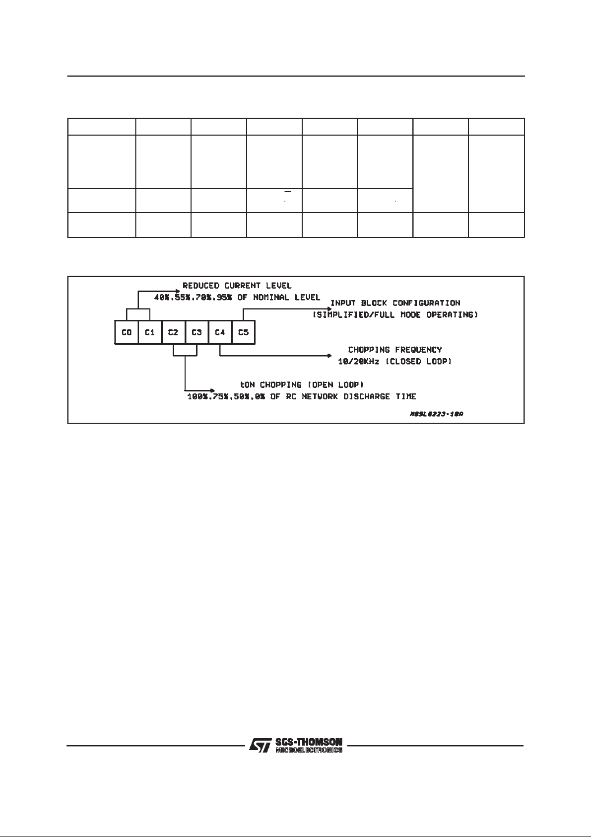
Figure 7 shows the six bit meaning.
In theoperating mode two different input drive are
possible. In SIMPLIFIEDOPERATING MODE the
IC needs few logic wire for the motor rotation, but
only the full step driving sequence can be performed.
7/33
Page 8
L6223
Table 1
Device status Bit C5 IN1 IN2 IN3 IN4 DA/CLEV DA/OPLO
Simplified
mode
operating
Full mode
operating
Programming
mode
Figure7:
L
H
XLLLL
Phase A
Driver
Phase A Phase A
Phase B
Driver
driver
InternalSix-Bit Shift Register Bit Functions
Enable
Phase B
driver
Alternative
Current
Reduction
”LOW”
Phase B
driver
Current
Reductio
Active
”HIGH”
serial
data in
Open/Closed
Loop current
control
serial
data in
CIRCUIT OPERATION
(continued)
The FULL OPERATING MODE permits all the
driving possibilities.The 4 low side DMOS transistors are drived directly by the 4 inputs IN1, IN2,
IN3, IN4 which define directly the phases configuration. The chopping of the motor current can be
in open loop or in close loop. When in open loop
(fixed on-time block) the DA/OPLO pin is High
and the motor current is not controlled but it
mostly depends from the bits C2 nd C3. When in
close loop the DA/OPLO is Low and the output
current is controlled at a constant value defined
by the internal reference and by the sensing resistor value. The internal reference depends by
the programming bits C0, C1, and by the input
configurations.During the power on sequencethe
reset circuitry prevents current spikes disabling
the outputsand by resettingthe memory.
Power Section
The basic concept for the current control is explained by examining the winding pair phase A
(MA) in Figure 24. With Q5 = ON, Q2 = OFF the
current rises until R
equals the comparator
SIP
thresholdvalue. The comparatoroutput resets the
8/33
F/F and Q5 switches off. In this condition the current decay path begins as shown in Figure 25.
The current value becomesI
/2, according to the
p
double number of turns interested. In order to reduce the dissipation, Q2 is also driven on. Q5 remains off (PWM off time) up to a new clock pulse
sets again the F/F.The winding current behaviour
is shown in Figure 26.
Since during PWM off time the current value is
half that of the on time and since in a typical application Toff >>Ton, the device dissipation is further reduced.
The five DMOS transistors are connected to the
”predriver stages” block, that drives the DMOS
gates, and interfaces them to the internal input
logic. The ”charge pump” provides correct voltage
for Q5 UPPER DMOS gate drive by using the external bootstrapcapacitor.
ProgrammingMode
The Programming Mode is defined by the inputs
IN1=IN2=IN3=IN4=Low. When in PROGRAMMING MODE the outputs are disabled. The waveform shown in Fig. 8 represents one possible tim-
Page 9
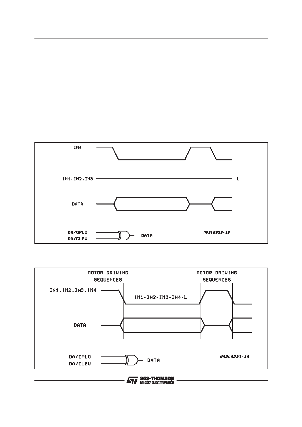
L6223
ing diagram for programming. When the inputs
IN1...IN4 are together Low a clock pulse is generated internally which clocks a data bit into the
shift register. If the time interval during which all
four inputs are Low is less than 0.2µs, no clocks
pulse in generated thus preventing undesirable
programming. To generateanother clock pulse at
least one of the four inputs must first go High and
then Low again. The first bit isloaded into C0 and
after 6 clock pulse it will be in the C5 posistion.
Two programming technique are suggested. The
first (Fig. 8) uses IN4 in such a way that the
Figure 8:
Wavefor mforprogrammi ng:the outputis disabledduringall theprogram mingduration(seeTable 4).
power section is disabled the total programming
time (the carriage of the 6 programmingbits). Fig.
9 shows another technique:the motor driving signals at the inputsIN1...IN4 are interrupted switching IN1...IN4 Low to carry a single bit. This permits the motor to be enabled for the 50% of total
programming time. During the motor rotation it’s
suggested to program the device immediately after the motor phase change: this make neglectable the motor driving discontinuity due to the device programming.
Figure9: Waveform for programming:theoutput is disabled only whenall four inputs are atthe low level.
9/33
Page 10

L6223
OperatingMode
The bit C5 defines the two available input configurations.
C5 = H: FULL MODE OPERATING
The digital inputshave the following functions:
•
IN1drives OUT1
•
IN2drives OUT2
• IN3drives OUT3
The output DMOS is ON
when the corrisponding input is low
• IN4drives OUT4
• DA/CLEVenablesthe current reduction
(seeTab 2)
•
DA/OPLOselectsthe motor current control
mode(open or closeloop).
Since each input drives one phase of the motor it
is possible to work either in Half Step or in Full
Step mode. DA/OPLO defines the current control
modeas follow:
– DA/OPLO = H open loop
– DA/OPLO = L closedloop
The reduced currentlevel is enabledby the inputs
IN1, IN2, IN3, IN4 or by DA/CLEV (Tab. 2). The
reduced current value dependsfrom the bits C0,
C1 (TAB. 5). The outputs are disabled when the
inputs are in a prohibited state (Tab. 4).
C5 = L, SIMPLIFIED MODEOPERATING
When in SIMPLIFIEDMODE OPERATINGthe in-
puts assumethe following functions:
•IN1 drivesPhase A
•IN2 drivesPhase B
•
IN3 ENABLE input (activeHigh)
•
IN4 enables the reduced current(Tab. 3)
•DA/CLEVenables the reduced current (Tab. 3)
• DA/OPLO selects the motor current control
mode
The SIMPLIFIED MODE OPERATING configura-
tion does not allow the drive of a unipolar motor in
Half step.
The signal DA/OPLO functions as in FULL Mode
Operation. When the current control is implemented in closed loop, the reduced current level
is enabled by the inputs IN4, DA/CLEV (Tab. 3).
The current reduction depends from the bits C0,
C1 (Tab. 5).
Open/ClosedLoopMotor Current Control
The logic input DA/OPLO selects the current control mode as previously seen. When in open loop,
the chopping frequency is that one as defined by
the external RC network. In open loop are available three different t(ON), dependingfrom the bits
C2, C3 (Tab. 6), as a percentage of the RC dischargetime t
(dis)
.
When in closed loop two different chopping frequencies are selectable by means of the bit C4
(Tab. 7). The higher is defined by the external RC
network. The other one is exactely the half. In
closed loop 5 different current levels are available: the nominal current level and four reduced
current levels (Tab. 5). The nominal current level
is set by an internal reference voltage of 0.5V.
The configuration of bits C0, C1 sets the reference voltage to a pecentageof the nominal value.
TRUTH TABLES
(L = Low; H = High; X = don’t
care)
Table 2
IN1 IN2 IN3 IN4 DA/CLEV C/R*
HHXX X H
XXHH X H
HHHH X H
XXXX H H
*) C/R = H,reduced current
Table 3
IN4 DA/CLEV C/R
LXH*
XHH*
H L L**
*) Reducedcurrent **) Nominal current
Table 4
IN1 IN2 IN3 IN4 Output Stage
L L X X DISABLED
X X L L DISABLED
Table 5
C0 C1 Reduced Current Level (*)
L L 40%
L H 50%
H L 70%
H H 85%
*) Nominal level percentage
10/33
Page 11

L6223
Table 6
C2 C3 t
LL75
LH50
H L 100
H H Output Disabled
(ON)/t(OSC)
*
Table 7
C4 Chopping Frequency
L 20kHz
H 10kHz
*) RC discharge time percentage
L6223 Operating Configuration vs. 6bits Shift Register Programming
(External RC network: R =
18kΩ C = 3,3nF)
SHIFT REGISTER bITS
Nr C5 C4 C3 C2 C1 C0
0 0 0 0 0 0 0 S 20 75 40%
1 0 0 0 0 0 1 S 20 75 70%
2 0 0 0 0 1 0 S 20 75 55%
3 0 0 0 0 1 1 S 20 75 85%
4 0 0 0 1 0 0 S 20 100 40%
5 0 0 0 1 0 1 S 20 100 70%
6 0 0 0 1 1 0 S 20 100 55%
7 0 0 0 1 1 1 S 20 100 85%
8 0 0 1 0 0 0 S 20 50 40%
9 0 0 1 0 0 1 S 20 50 70%
10 0 0 1 0 1 0 S 20 50 55%
11 0 0 1 0 1 1 S 20 50 85%
12 0 0 1 1 0 0 S 20 DISABLED 40%
13 0 0 1 1 0 1 S 20 DISABLED 70%
14 0 0 1 1 1 0 S 20 DISABLED 55%
15 0 0 1 1 1 1 S 20 DISABLED 85%
16 0 1 0 0 0 0 S 10 75 40%
17 0 1 0 0 0 1 S 10 75 70%
18 0 1 0 0 1 0 S 10 75 55%
19 0 1 0 0 1 1 S 10 75 85%
20 0 1 0 1 0 0 S 10 100 40%
21 0 1 0 1 0 1 S 10 100 70%
22 0 1 0 1 1 0 S 10 100 55%
23 0 1 0 1 1 1 S 10 100 85%
24 0 1 1 0 0 0 S 10 50 40%
25 0 1 1 0 0 1 S 10 50 70%
26 0 1 1 0 1 0 S 10 50 55%
27 0 1 1 0 1 1 S 10 50 85%
28 0 1 1 1 0 0 S 10 DISABLED 40%
29 0 1 1 1 0 1 S 10 DISABLED 70%
30 0 1 1 1 1 0 S 10 DISABLED 55%
31 0 1 1 1 1 1 S 10 DISABLED 85%
32 1 0 0 0 0 0 F 20 75 40%
33 1 0 0 0 0 1 F 20 75 70%
34 1 0 0 0 1 0 F 20 75 55%
35 1 0 0 0 1 1 F 20 75 85%
36 1 0 0 1 0 0 F 20 100 40%
37 1 0 0 1 0 1 F 20 100 70%
38 1 0 0 1 1 0 F 20 100 55%
Full/Simpl.
Operation
Mode
Close Loop
Frequency
(kHz)
Open Loop
t
[%]
(ON)
Close Loop
Current
Level [%]
11/33
Page 12

L6223
L6223 OperatingConfiguration vs. 6bits Shift Register Programming
SHIFT REGISTER bITS
Nr C5 C4 C3 C2 C1 C0
39 1 0 0 1 1 1 F 20 100 85%
40 1 0 1 0 0 0 F 20 50 40%
41 1 0 1 0 0 1 F 20 50 70%
42 1 0 1 0 1 0 F 20 50 55%
43 1 0 1 0 1 1 F 20 50 85%
44 1 0 1 1 0 0 F 20 DISABLED 40%
45 1 0 1 1 0 1 F 20 DISABLED 70%
46 1 0 1 1 1 0 F 20 DISABLED 55%
47 1 0 1 1 1 1 F 20 DISABLED 85%
48 1 1 0 0 0 0 F 10 75 40%
49 1 1 0 0 0 1 F 10 75 70%
50 1 1 0 0 1 0 F 10 75 55%
51 1 1 0 0 1 1 F 10 75 85%
52 1 1 0 1 0 0 F 10 100 40%
53 1 1 0 1 0 1 F 10 100 70%
54 1 1 0 1 1 0 F 10 100 55%
55 1 1 0 1 1 1 F 10 100 85%
56 1 1 1 0 0 0 F 10 50 40%
57 1 1 1 0 0 1 F 10 50 70%
58 1 1 1 0 1 0 F 10 50 55%
59 1 1 1 0 1 1 F 10 50 85%
60 1 1 1 1 0 0 F 10 DISABLED 40%
61 1 1 1 1 0 1 F 10 DISABLED 70%
62 1 1 1 1 1 0 F 10 DISABLED 55%
63 1 1 1 1 1 1 F 10 DISABLED 85%
Full/Simpl.
Operation
Mode
Close Loop
Frequency
(kHz)
(Continued)
Open Loop
t
[%]
(ON)
Close Loop
Current
Level [%]
APPLICATION INFORMATION
SingleDevice Application
Figure 10 shows a typical Single Device Application. With the shown external RC network, the
higher choppingfrequencyis 20 kHz.
In the figure 11, 12 and 13 are shown the waveforms required to drive the motor in Half/Full Step
in FULL MODE OPERATING (FMO) and SIMPLIFIED MODE OPERATING (SMO). The sense resistor defines the total motor current. This means
that when two phases are ON, the sense current
is two times the phase current. In this case the
sense resistor value is R
S
=(V
ref
/2Ip), where V
ref
is the reference voltage and IPthe phase current.
We have supposed that the phase current is of
the same intensity in the two phases. When only
one phase in ON, the current flowing in the sensing resistor is the phase current: this occurs in
half step driving mode. The Figures 14 and 15
show the envelope of the sensing voltage in full
and half step respectively.
When current imbalance is not considered, this
12/33
envelope represents the current level 2I
control-
p
led by the chopping when L6223 is working at
100% of current; in full step this level is constant
while in half step two different levels are present
(Figure 15). Actually, in full step two phases are
alwaysON, and the chopping current levelcan be
changed only by the controller. In half step when
two phases are ON and L6223 is working at
nominal current level (2I
), but when only one
p
phase is ON, L6223 selects automatically the reduced current. This level depends upon the programming bits. In Figure 15 the higher level represents the chopping at nominal value (two
phases ON), the lower level the chopping at the
reduced current (one phase ON). The negative
peak shown in the figures represents the fast current recirculationat the phase change.
Fig. 15 shows also what happens when the reduced current level selected is at 70% of the
nominalvalue. The motor torque is proportionalto
the vectorial sum of the phase currents: it can be
seen that the unipolar stepper motor control actuated by L6223 in half step is at constant torque
but not at constat current.
Page 13

L6223
Figure10:
TypicalApplicationCircuitusing a singledevice:the max peakcurrent capabilityis of 1A/phase
=0.25Ω)
(R
S
Figure11:
Inputsfor Half Stepdrive, single device
FMO.
Figure13: Inputsfor Full Step drive singledevice SMO.
Figure12:
Inputsfor Full Step drive, single device
FMO.
13/33
Page 14

L6223
Figure14:
Peakcurrent 2I
crossingthe sense resistorRSin Full step drive. The phase sequenceCCW
p
is: AB →BA →AB → BA (4 Full Steps, 2 phase ON)
Figure15: Peakcurrent(2I
resistorR
S
/2phaseON)andreducedpeakcurrent(1.4Ip/1phaseON)crossingthesense
p
in Halfstep drive. The phasesequence is: A→AB
→ B →
BA→A→AB→B→BA
(8 Half Steps,1 phaseON and 2 phasesON alternatively)
Figure 16: Typical Application Circuit using 2 devices (Paralleled configuration): the max peak current
capabilityis of 2A/phase(R
= 0.25Ω)
S
14/33
Page 15

L6223
Dual Device Application
Fig. 16 shows how to drive one unipolar stepper
motor by means of two L6223 Each device drives
one phase of the motor. This permits doubling of
the phase current. Since in this configuration
each sense resistor controls the phasecurrent (in
Single only one sense resistor controls the total
=(V
motor current), we have: R
S
/Ip) where V
ref
ref
is the voltage reference and Ip the phase current
in the Dual that is coincident with the chopping
Figure17: Inputsfor Half Step drivedual device SMO.
current. The configuration in the figure shows the
only possible way to parallel two L6223. The use
of another configuration can cause serious demage to the IC during the programming. The
waveforms required to drive the motor in half/full
step are shown in Fig. 17 and 18: as it can be
seen, the two L6223 are in SIMPLIFIED MODE
OPERATING configuration. The half step drive
can be achieved by driving the inputs IN3 which
are ENABLEinputs.
Figure18:
Inputsfor Full Step drive singledevice SMO.
Dot Matrix Printer MotorDriver
Fig. 19 shows how to drive the paper feed and
the carriage motors by means of 3 L6223 using a
very low wire number. The carriage motor is
driven by two paralleled L6223, the paper feed
motor, which requires a lower current, uses one
L6223. The three ICs are working in SIMPLIFIED
MODE OPERATING. The inputs IN1-IN2, IN3 are
driven as previously seen (Single and Dual Device configuration). The inputs IN4 and DA/CLEV
are grounded so that the ICs work in reducedcurrent levels. This means L6223 can select seven
current levels through programming: four in
closed loop and three in open loop. The input
DA/OPLO is used to load the programming data;
only the device in PROGRAMMING MODE is programmed. The two paralleled L6223 can deliver
up to 2A/phasewhilethe single L6223, 1A/phase.
15/33
Page 16

L6223
Figure19:
Dot MatrixPrinter Motor Driver schematicdiagram (See also fig. 10, 16).
ExternalRC Network (pin 14)
The external RC network provides the higher of
the two possible chopping frequencies. The discharge time of the capacitor represents the minimum t
is possible to select a smallert
available in closed loop. In open loop it
(ON)
, (see Fig. 20).
(ON)
The t
min defines the min current the IC can
(ON)
supply to the motor, as well as the protection
”window”. This window is necessary to mask the
spike generated at the beginning of each chopping period (see Fig. 21a).
Figure20: Oscillator waveformand timing.
The window must be large enough to mask this
spike, without penalizing excessively the min current control. The capacitor C mainly defines the
value of the window. The mathematical formulas
to calculatethe approximatevaluesare:
f
= 1/(0.84 • RC) for R > 10kΩ
(osc)
t
ON(min)=t(window)
for R
where R
= 1.2kΩ
in
is the resistor internal to the IC for the
in
= 0.84 • C •R • Rin/(R+Rin)
capacitordischarging.
16/33
Page 17

L6223
Figure21a:Relati ons hi pbetweencapacitordischar ge
oftheoscillator ,windowandsensingvoltage
Figure21b: Oscillatorbehaviourof the L6223 and
of theL6223 (simplifiedwaveforms).
The behaviour of the oscillator at each phase
change allows the L6223 to drive high speed
unipolarstepper motors.
This is the main functionaldifference between the
L6223 and the L6223 (see fig. 21b).
In the latter, the phase change starts only when
the clock pulse sets the F-F (Fig. 22) that is when
the capacitor voltage reaches the discharge
threshold.
As a result, a variable delay between the leading
edge of the input signal and the beginning of the
currentdecay to zero can be expected.
Because of that, driving high speedy stepper motors is produced a noisy beating between chopping frequencyand phase change rate.
In the L6223 as soon as the phase change is
driven by the inputs, the oscillator voltage Jumps
to its top level, a new discharge period is generated and the chopping transistor is switched ON
(Q5 in fig. 22). The advantages are a motor
phase change synchronous to the driving signal
and no beating for whatever rotation speed. By
setting pin 14 at a voltage equal or less than Vrs
= 0.9V, when the IC is normally supplied and the
oscillator is running, the 6 bit shift register is
quickly reset and the power outputs are disabled:
a delay of 700nsec max mustbe expected.
The use of this behaviour to reset the device at
the turn-on is not allowed; however the reset is
automatically provided by the Logic Supply Voltage crossing the threshold of 3.5V (typ.) both at
the turn-ONand at the turn-OFF.
Protection
The protection zeners on the outputs protect the
IC from overvoltage during chopping and phase
change. Actually, at the phase change, the outputs rise to a voltage equal to V
where V
is the power supply and Vmthe product
S
=2VS+Vm,
O
of the motor resistance Rm with the peak phase
current Ip. Vs is doubled because in the unipolar
motor we have two coupled phases connected in
series(phase A and A, B and B) for each of the
two windings of the motor (MA, MB see Fig. 22).
The leakageinductance,seen from the outputs of
the L6223, can generate an overvoltage higher
than V
. To protect the IC, the zeners must be
O
able to sustain a power of 400W for 1 microsec
and must be able to conduct at a voltage V
higher than V0=2V
s(max)+Vm
. It’s importantthat
during the transition, at the max operating ambient temperature, the zener conduction is guaranteed for a voltage lower than 125V (see Absolute
Max Ratings). The ST-BZWO4-85 satisfies this
requirement. The diode connected to the common protects this input from the undergounds due
to the leakage inductances and/or the imbalancing between the phase currents.
z
17/33
Page 18

L6223
Figure22:
Poveroutput configuration.
Use of the ProgrammingMode
A typical application of the L6223 requires driving
the motoraccording to Fig. 23a andFig. 23b.
Starting from t
tor is kept in stand-by;at time t
eration period that is completed at time t
and continuinguntil t1themo-
0=t5
beginsan accel-
1
. The
3
motor then is driven at a contant speed until t
when the speed is decelerated and is stopped at
t
for a new standbyperiod.
5=t0
During these events the L6223 can be programmed several times for different working
modes. The most important parameter is the current through the windings of the stepper: at the
time t
0;t1;t2;t3
and t4the current can be modified, for example, as it is shown in Fig. 23b. This
behaviour allows the best motion control and, at
the same time, optimizes efficency of the power
output block of the I. C.
But this is not the best in terms of performances
by programming:in fact, betweent
and t5thede-
1
vice can be programmed to work in Closed Loop
and to chop at half of the RC oscillator frequency
during the time t
to t4. In the stand-by condition
3
the I. C. can be programmed to work in Open
Loop mode where the current can be fixed by the
reduction of the minimum T
time (75% or 50%)
ON
defined by the dischargetime of the RC oscillator.
Of course in this way the current can be modified
by Supply Voltage changes; the same is not possible in Closed Loop operation where the device,
in order to keep the windings current constant,
modifies the T
at high V
. This is the reason why when the motor
S
is driven at a constant speed (t
time: wide at low VSand narrow
ON
to t4) with small
3
current and high Supply Voltage, it could become
necessary to program the lower chopping fre-
quency to allow a suitable T
width otherwise
ON
the current of the windings would go out of control.
The motion profile, shown in Fig. 23a can be obtained when preferred, with only two program
changes actuated while the motor is in stand-by.
The current becomes as shown in Fig. 23c. The
device can be programmed at t
55% (stand-by) and at t
1
for I
0=t5
= 70%: for both
motor
the actuations,the DA/CLEVis kept high to allow
the program change, while, by keeping it to zero
during t
and t4-t5, the current is automat-
1-t3
ically select as 100% (Fig. 23d). During t
current is reduced according to the percentage
programmedat the time t
.
1
Power dissipation (Simplified method of calculation).
Here below the Full Step Operating Mode is considered; in addition, the following working conditions have been taken up:
1) Constant speed rotation of the driven unipolar
stepperMotor.
Figure23: a,b) Speed profileand motorcurrent
controlchange for the best efficencyof the I.C.
c,d) Current control change by using DA/CLEV
input only, duringthe stand-byperiod.
,
4
for I
3-t4
motor
=
the
a
b
c
d
18/33
Page 19

L6223
2) Back EMF (BEMF) equal to 80% of its peak
during the phase change and equal to 50% of its
peak during the choppingperiod.
3) Constant slope of the current during t
ON,tOFF
and for power calculation during the phase
change (See t
in Fig. 27).
1
4) Current imbalancesupposed to be zero.
5) Current ripple during the chopping neglegible.
As was previously stated, the current chopping is
obtained by means of one PWM Loop that controls the charge time t
of the inductance of the
ON
windings, A and B for example in fig.22.
This time starts each clock pulse and stops when
Q5 is switched OFF becauseof thecondition:
=2RSIp.
V
ref
A factor 2 is required because the single sensing
resistor R
is crossedby the peak current Ipflow-
S
ing through each of the two energized windings
(A of MA; B of MB).
This configuration can produce an imbalance between the two peak currents because at the
phase change the BEMF of one winding (MA) can
be out of phase with respect to the BEMF of the
other one (MB); in addition, an imbalance may
also occur at the phase change when the Power
Supply Voltage selected is too low and/or when
one motor is drivenwith too large Lm/Rm ratio.
Neverthelessin most of the applications the dissipated power is not increased and there is no significant change in torque.
During t
phase A (seg. Fig. 24), is defined by V
VON≅ VS-R
where R
the current Ip, flowing through the
ON
Ip - BEMF
tot
tot=RS+Rm+RDSON tot
ON
in which Rmis the winding resistance of the
phase A and R
Q1 and Q5: R
DSON tot
m
is the sum of the R
DSON
of
and BEMF are not shown on the
Figure 24.
At the end of t
and jumps to I
ductance becomes four times L
, the current starts its slow decay
ON
/2 (see Fig. 25) since the total in-
p
(perfect cou-
m
pling) that is the inductanceof the phase A alone.
The recirculationtime t
V
≅ 2BEMF+ IP(Rm+R
OFF
since R
DSONQ1=RDSONOQ2
is defined by:
OFF
DSONQ1
.
)
The current through Q1 is shown in Fig. 26: the
current ripple is on lp and I
/2 during tONand t
P
OFF
respectively.It can be obtained the Duty Cycle:
DC = V
since 2V
/ (2VON+V
OFF
ONtON=VOFFtOFF
OFF
)
The slow decay allows a small current ripple as
earlier It is considered equal to zero. The current
through the phases A and B can be seen in Fig.
27 where the InA and InB signals (see Fig. 22)
are shown as well.
These two signals are 90° out of phase with each
other and they are 180° out of phase with the corresponding inputs of the IC. In A and In B are not
shownin the Figure.
During the time Tp the motor goes through four
steps and the rotation speed V
(step/sec) can
rot
be given by:
V
= 4/Tp.
rot
By consideringwhat was stated above, the following can be applied:
1) Dissipated power by the 4 sink power DMOS
(Q1to Q4).
PdL ≅
4R
DSONQ1
T
P
2
I
p
T
T
1
+
3
2
1 +
p
+
T
1
DC
2
2) Dissipated power by Q5 (PdH).
PdH ≅ 4R
DSONQ5
2
DC
I
p
T
4
1
+
− 4DC
T
3
p
wherethe phase change duration is:
log
−
1
e
Vs− 1.6 BEMF + R
2R
totIp
L
m
= −
T
1
R
tot
tot
I
P
The chopping produces little power dissipation.
It’s value can be approximatedby:
-3
3) Pdch ≅ 8 ⋅ 10
VsI
p
The sum of 1) + 2) + 3) gives the dissipated
power of the output stage. To obtain the total
amount of dissipated power it’s necessary to include the power dissipation produced by the quiescent currents I
(from the power stage) and I
S
SS
(fromthe Logicalcircuits):
P
do=VSIS+VSSISS
consideringI
P
= PdL+ PdH + Pdch+ Pdo
tot
S
,
constatversusVS. Finally:
Example
SupplyVoltage V
Logic Voltage V
Peak current (per phase)I
Motorresistance R
Motorinductance L
Rotationspeed V
=36V
S
=5V
SS
= 0.7A
p
=9Ω
m
=6mH atT
m
= 500step/sec(const)
rot
amb
=50°C
Peak of the BEMF BEMF = 1 Vp
Max ambient temperature T
Max junction temperature T
=50°C
amb
=125°C
j
Fromthe ElectricalCharacteristicsof the L6223
(Typicalvalue):
InternalReference VoltageV
SinkDMOS R
DSON
SourceDMOSR
R
DSON
DSONRDSON
PowerSupply Current I
Logic Supply Current I
= 0.5V
ref
L = 1.2Ω at
H = 0.7Ω Tj= 25°C
= 4 mA Worst
S
= 20 mA Case
SS
FromFig. 3 (see pag. 6) the following is obtained:
≅
1.65 at Tj = 125°C.
α
TheDMOS ON-Resistancesbecome(worst case):
19/33
Page 20

L6223
R
R
R
R
V
V
DC= 15.6%
T
T
PdL = 1.1W
PdH = 0.4W
Pdch = 0.20W
Pdo = 0.24W
At last:
P
The neededthermalresistance betweenjunction
and ambient mustbe equal to:
L=α1.2= 2Ω
DSON
H=α0.7 = 1.15Ω
DSON
= 0.36Ω
S
= 12.5Ω
tot
= 26.24V (During the chopping)
ON
= 9.7 (Duringthe chopping)
OFF
=8 msec
p
=250µs (During the phase change)
1
= 1.94W
tot
T
thj−amb
=
P
tot
R
The worst case here considered requires an
jmasc−Tambmasc
≅
39°C/W
heatsink of 25°C/W. The calculation of the power
dissipation by considering the current imbalance
and by simulating a typical motion needed to
carry the head of a printer for example, becomes
full of difficulties. The use of the Personal Computer is helpful in such a case: few examples are
shownfromFig. 28ab untilFig. 31 ab.
Each figure shows the Application Datas and one
diagram where the Total Dissipated Power versus
the peak of themotor current is plotted.
A max Ambient temperature of 70°C and a max
junction temperature of 150°C have been considered for a few applications using one single device and a dual device configuration to drive one
Figure24: Motor current Ip during t
Figure25:
Slow decay of the motor currentI
(phaseMA; Q5 and RSsre common whit the phase MB).
ON
/2 during t
p
(phaseMA).
off
20/33
Page 21

L6223
steppermotor in the Full Step Mode.
The calculations consider three different conditions of heatsinking: the package with minimum
dissipating copper area on the p.c.b. (R
thj-amb
55°C); the copper side of 6 cm
40°C/W - See Fig. 34) and the additional heatsink
(R
thj-amb
=30°C/W).
=
Figure26: Phase current waveformduring chopping: the current decayduring t
OFF
is halved.
2
(R
thj-amb
Figure 27: Simplifiedwaveformsof the currentthrough the phase A (winding MA) and through the phase
B (winding MB). See also fig.22.
=
21/33
Page 22

L6223
Figure28a:
Single L6223 slow speed, ApplicationData.
Figure 28b: Total Power Dissipation. The vertical indicator tells us the max value of the current we can
supplyto the windings (Ip = 0.8A).The peakcurrentcorrespondingto the flat side ofeach of
the three shown trends is not allowed
22/33
Page 23

L6223
Figure29a:
Single L6223 high speed, ApplicationData.
Figure 29b: Total Power Dissipation.
23/33
Page 24

L6223
Figure30a: DualL6223 slow speed, Application Data.
Figure 30b:
Total Power Dissipation.
24/33
Page 25

Figure31a: DualL6223 high speed, Application Data.
L6223
Figure 31b:
Total Power Dissipation.
25/33
Page 26

L6223
Matchingthe L6223 with the motor.
For the correct design of the application the followingnotes must be considered.
* For low motor resistance and high supply volt-
age the L6223 minimum duty cycle may limit
the minimum current at a value higher than requested.
In this case we suggest to reduce the window
protection time changing the RC oscillator network. (See Fig. 21a and External RC Network).
* Only in single device application, for very low
motor resistance, a large current imbalance
may affect the correct motor rotation. Motor resistance value higher than 7 Ohm are generally
recommendedfor 35V PowerSupply.
* The correct motor winding execution is very im-
portant for the motor and the L6223 efficiency.
A simple test is the measurement of the stray
inductance between the central tap and the
ends shorted together of each winding. Theoretically the inductance would be zero; values
higherthan 50µH may show poor motor quality.
Computer Aided Development Board
An improvement in the application development
and in system debugging can be obtained by
meansof the PersonalComputer.
Interfacing the appliction with the PC, the motor
can be driven directly by this in real time operation. This permits the testing in very short time
and a lot of different motion configurations,during
application debugging and optimization. Moreover, by paralleling more application boards, an
efficientreliability test can be implemented.
The development board designed to drive L6223
in Single and Dual Device configuration is shown
in Fig. 32a-b. Fig. 33 is the corresponding electrical circuit. On the board are mounted three
L6223: two for the Dual Device configuration and
one for the Single Device. The three connectors
J1, J2, J3 allow the application board to be interfaced with the PC and to be paralleled with another one. The remaining connectors provide the
interface with the motor and the power and logic
supply. The ground area has been sized to act as
heatsink (35 micron thickness). When the copper
area is not sufficient to dissipate the heat an external heatsinkis required.
26/33
Page 27

Figure32a: L6223p.c.b. (componentsside).
L6223
27/33
Page 28

L6223
Figure32b:
L6223 p.c.b. (backside).
28/33
Page 29

L6223
Figure33:
L6223 Development Board schematicdiagram.
29/33
Page 30

L6223
Figure 34:
with two ”on board”square heatsink vs. side I.
R
th
Figure35: Transient thermal resistance for single pulses
Thermalcharacteristics.
The p.c.b. copper size needed for a definedthermal resistance between junction and ambient is
estimate the typical thermal resistance junction to
ambient for a single pulse of peak power and for
a repetetivepeak respectively.
shownin Fig. 34. Fig. 35 and Fig. 36 are useful to
30/33
Page 31

Figure 36: PeaktransientRth pulsewidth and DutyCycl e.
L6223
Notes on the p.c.b. design.
We recommend to observe the following layout
rules to avoid application problems associated
with ground loops and anomalous recirculation
currents. The by-pass capacitors for the power
and logic supply must to be kept as close to the
IC as possible.
It’s important to separate on the PCB board the
logic and the power grounds avoiding that
grounds traces of the logic signals cross the
ground traces of the power signals. The starpoint
grounding, the point of the board in which the
logic ground meets the power ground, should be
kept far enough away from where the power
ground traces terminate to ground (sense resistors and protection zener diodes traces). This
avoids interference with the logic signals. Be-
cause the IC uses the board as a heatsink the
dissipating copper area must be sized in accordance with the requiredvalue of R
thj-amb
. It’s important to provide a good filter for the logic supply,
especially for the resistor of the oscillator network. In addition, the capacitor ground of the RC
network must be as clean as possible. When the
ground is used also to heatsink, it is helpful to
use either a polistyrin capacitor or one with a low
temperature coefficient. The value of the bootstrap capacitor is not a critical parameter, nevertheless the use of a capacitor of 10nF±20% is
recommended. A non-inductive resistor is the
best way to implementthe sensing, but when that
is not possible, more metalfilm resistors of the
same value canbe paralleled.
31/33
Page 32

L6223
POWERDIP20 PACKAGEMECHANICAL DATA
DIM.
MIN. TYP. MAX. MIN. TYP. MAX.
a1 0.51 0.020
B 0.85 1.40 0.033 0.055
b 0.50 0.020
b1 0.38 0.50 0.015 0.020
D 24.80 0.976
E 8.80 0.346
e 2.54 0.100
e3 22.86 0.900
F 7.10 0.280
I 5.10 0.201
L 3.30 0.130
Z 1.27 0.050
mm inch
32/33
Page 33

L6223
Information furnished is believed to be accurate and reliable. However, SGS-THOMSON Microelectronics assumes no responsibility for the
consequences of use of such information nor for any infringement of patents or other rights of third parties which may result from its use. No
license is granted by implication or otherwise under any patent or patent rights of SGS-THOMSON Microelectronics. Specification mentioned
in this publication are subject to change without notice. This publication supersedes and replaces all information previously supplied. SGSTHOMSON Microelectronics products are not authorized for use as critical components in life support devices or systems without express
written approval of SGS-THOMSON Microelectronics.
1998 SGS-THOMSON Microelectronics – Printed in Italy – All Rights Reserved
SGS-THOMSON Microelectronics GROUP OF COMPANIES
Australia - Brazil - Canada - China- France - Germany - Italy - Japan - Korea - Malaysia - Malta - Morocco - The Netherlands -
Singapore - Spain - Sweden - Switzerland - Taiwan - Thailand - United Kingdom - U.S.A.
33/33
 Loading...