

Page 1
ABLE TO DRIVE BOTH WINDINGS OF BIPOLAR STEPPER MOTOR
OUTPUT CURRENT UP TO 750mA EACH
WINDING
WIDEVOLTAGERANGE 10V TO 46V
HALF-STEP, FULL-STEP AND MICROSTEPP-
INGMODE
BUILT-INPROTECTIONDIODES
INTERNALPWM CURRENT CONTROL
LOW OUTPUTSATURATIONVOLTAGE
DESIGNED FOR UNSTABILIZED MOTOR
SUPPLYVOLTAGE
INTERNALTHERMAL SHUTDOWN
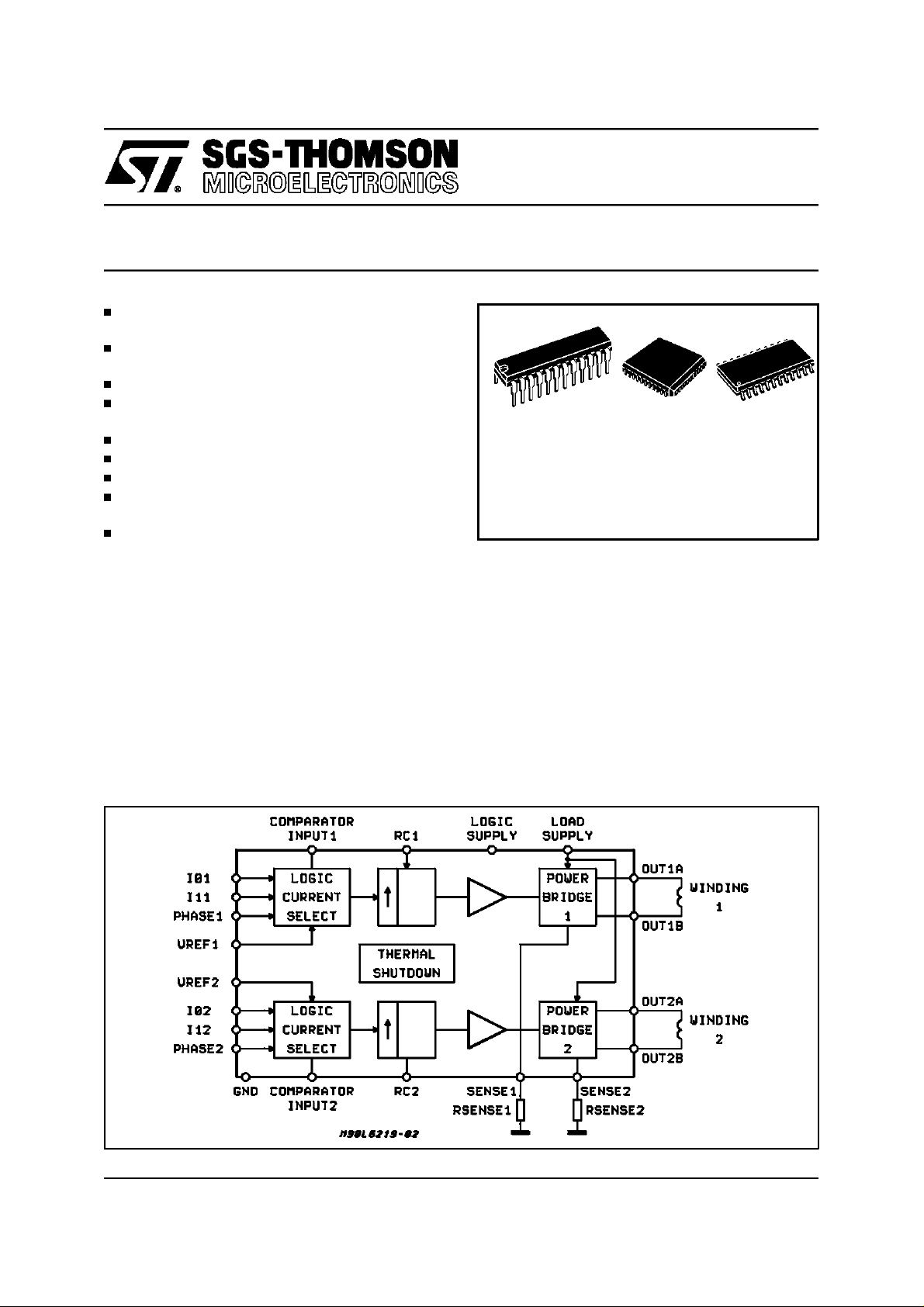
DESCRIPTION
The L6219 is a bipolar monolithic integrated circuits intended to control and drive both winding of
a bipolar stepper motor or bidirectionally control
two DC motors.
The L6219 with a few external components form
a complete control and drive circuit for LS-TTL or
microprocessorcontrolledstepper motor system.
The power stage is a dual full bridge capable of
sustaining 46V and including four diodes for current recirculation.
A crossconductionprotection is providedto avoid
L6219
STEPPER MOTOR DRIVER
Powerdip 20+2+2 PLCC44 SO20+2+2
ORDERING NUMBERS:
L6219 L6219D L6219DS
simultaneous cross conduction during switching
currentdirection.
An internal pulse-width-modulation (PWM) controls the output current to 750mA with peak startup current up to 1A.
Wide range of current control from 750mA (each
bridge) is permitted by means of two logic inputs
and an external voltage reference. A phase input
to each bridge determines the load current direction.
A thermal protection circuitry disables the outputs
if the chip temperature exceeds safe operating
limits.
BLOCK DIAGRAM
December 1996
1/10
Page 2
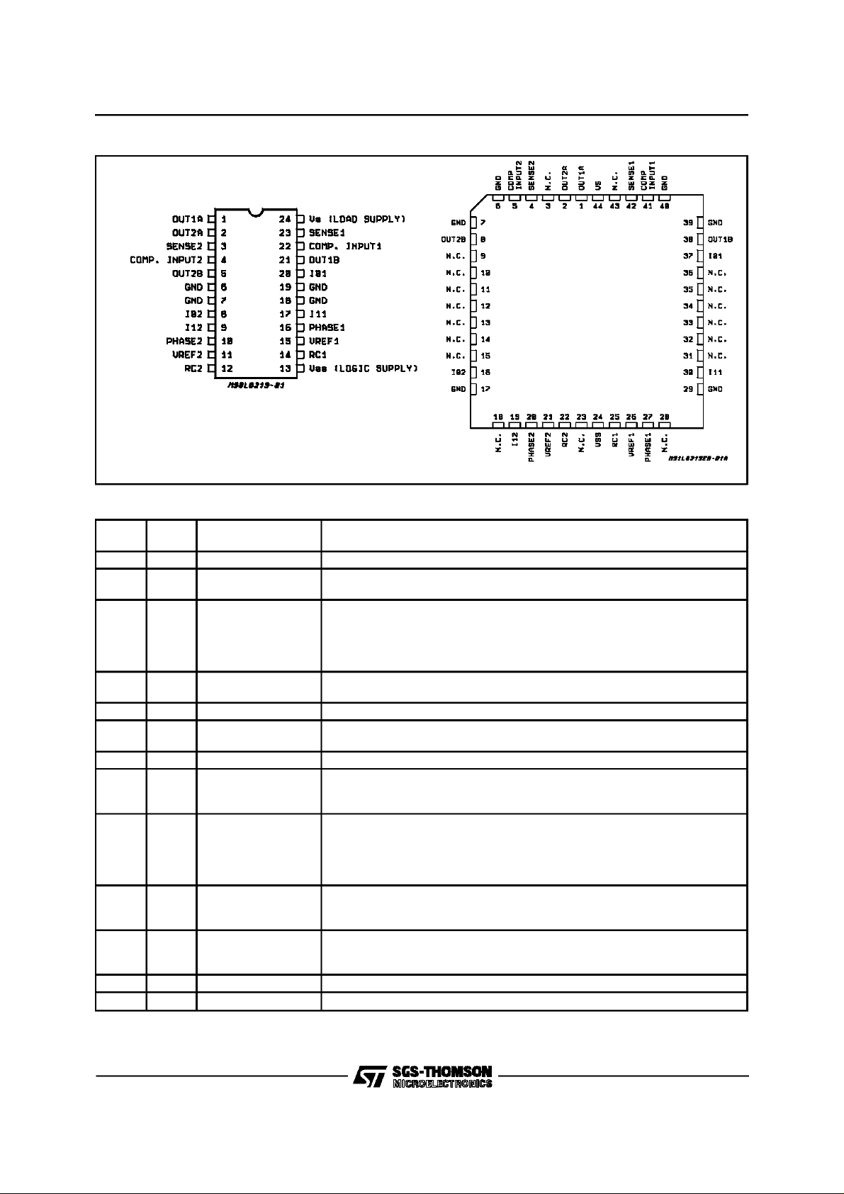
L6219
PIN CONNECTIONS (Topview)
Powerdip and SO
PIN FUNCTIONS
PLCC44
PLCC
(*)
PDIP &
SO
Name Function
1;2 1;2 OUTPUT A See pins 5;21
4;42 3;23 SENSE RESISTOR Connection to Lower Emitters of Output Stage forInsertion of Current Sense
Resistor
5;41 4;22 COMPARATOR
INPUT
Input connected to the comparators. The voltageacross the sense resistor is
feedback to this input throught the low pass filter RC CC. The higher power
transistors are disabled when the sense voltage exceeds thereference
voltage of the selected comparator.When this occurs the current decays for
a time set by R
TCT(toff
= 1.1 RTCT). See fig. 1.
8;38 5;21 OUTPUT B Output Connection. The outputstage is a ”H” bridge formedby four
transistors and four diodessuitable for switching applications.
6;7;17 6;19 GROUND See pins 7;18
29;39;407;18 GROUND Ground Connection.With pins6 and 19 also conducts heatfrom die to
printed circuit copper.
16;37 8;20 INPUT 0 See INPUT 1 (pins 9;17)
19;30 9;17 INPUT 1 These pins and pins 8;20 (INPUT 0) are logicinputs which select the outputs
of the comparators to set the current level.Current also depends on the
sensing resistor and reference voltage. See FuncionalDescription.
20;27 10;16 PHASE This TTL-compatible logic inputssets the direction of current flowthrough
the load. A high levelcauses current to flow from OUTPUT A (source)to
OUTPUT B (sink). A schmitttrigger onthis input provides good noise
immunity and adelay circuit prevents output stageshort circuits during
switching.
21;26 11;15 REFERENCE
VOLTAGE
A voltage applied to thispin sets the reference voltage of the comparators,
this determining the outputcurrent (also thus dependingon R
and the two
s
inputs INPUT 0 and INPUT 1).
22;25 12;14 RC A parallel RC network connected to this pin sets the OFF time ofthe higher
power transistors. The pulsegenerator is a monostable triggered by the
24 13 V
output of thecomparators (t
- LOGIC SUPPLY Supply Voltage Input for Logic Circuitry
ss
= 1.1 RTCT).
off
44 24 Vs - LOAD SUPPLY Supply Voltage Input forthe Output Stages.
(*)Pins: 3, 9,10,11,12,13,14,15,18,23,28,31,32,33,34,35,36,43 are Not Connected.
Note: ESD on GND, V
, OUT 1A and OUT 2Ais guaranteedup to 1.5KV (Human Body Model, 1500Ω, 100pF).
S,VSS
2/10
Page 3
ABSOLUTE MAXIMUM RATINGS
Symbol Parameter Value Unit
Supply Voltage 50 V
S
Output Current (peak) ±1A
I
o
Output Current (continuous) ±0.75 A
I
o
Logic Supply Voltage 7 V
SS
Logic Input VoltageRange -0.3 to +7 V
IN
Sense Output Voltage 1.5 V
Junction Temperature +150
J
Operating Temperature Range 0 to 70 °C
op
Storage Temperature Range -55 to +150 °C
stg
V
V
V
V
sense
T
T
T
THERMAL DATA
Symbol Description PLCC PDIP SO Unit
R
thj-case
R
thj-amb
(*) With minimized copper area.
Thermal Resistance Junction-case Max.
Thermal Resistance Junction-ambient Max.1245 (*)1460 (*)1875 (*)
L6219
C
°
°C/W
C/W
°
ELECTRICALCHARACTERISTICS (Tj=25°C,VS= 46V, VSS= 4.75Vto 5.25V, V
= 5V; unlessoth-
REF
erwise specified)See fig.3.
Symbol Parameter Test Condition Min. Typ. Max. Unit
OUTPUTDRIVERS (OUTAor OUTB)
I
V
CE(sat)
I
S(on)
I
S(off)
V
CEX
I
V
Motor Supply Range 10 46 V
S
Output Leakage Current V
Output Saturation Voltage Sink Driver, I
Clamp Diode Leakage Current VR = 50V - <1 50 µA
R
Clamp Diode Forward Voltage SinkDiode
F
=Vs
OUT
V
=0
OUT
Sink Driver, I
OUT = +750mA
Source Driver, I
Source Driver, I
Source Diode I
= +500mA
OUT
OUT
OUT
=750mA
F
= -500mA
= -750mA
-
-
-
-
-
-
<1
<-1
0.3
0.7
1.1
1.3
1
1
Driver Supply Current Both Bridges ON, No Load - 8 15 mA
Driver Supply Current Both Bridges OFF - 6 10 mA
50
-50
0.6
1
1.4
1.6
1.5
1.5
CONTROLLOGIC
V
IN(H)
V
IN(L)
I
IN(H)
I
IN(L)
V
REF
I
SS(ON)
I
SS(OFF)
Input Voltage All Inputs 2.4 - - V
Input Voltage All Inputs - - 0.8 V
Input Current VIN = 2.4V - <1 20 µA
Input Current VIN = 0.84V - -3 -200
Reference Voltage Operating 1.5 - 7.5 V
Total Logic Supply Current Io=I1= 0.8V, No Load - 64 74 mA
Total Logic Supply Current Io=I1= 2.4V, No Load - 10 14 mA
COMPARATORS
µ
µA
µ
A
V
V
V
V
V
V
A
V
REF/Vsense
t
off
t
d
Current Limit Threshold (attrip
point
Cutoff Time Rt = 56KΩ Ct= 820pF - 50 s
Turn Off Delay Fig. 1 - 1 s
Io=I1= 0.8V 9.5 10 10.5 -
= 2.4V, I1= 0.8V 13.5 15 16.5 -
I
o
= 0.8V, I1= 2.4V 25.5 30 34.5 -
I
o
µ
µ
3/10
Page 4

L6219
ELECTRICALCHARACTERISTICS(Continued)
Symbol Parameter Test Condition Min. Typ. Max. Unit
PROTECTION
T
J
Figure 1
Thermal Shutdown Temperature - 170 - °C
FUNCTIONAL DESCRIPTION
The circuit is intended to drive both windings of a
bipolar steppermotor.
The peak current control is generated through
switch mode regulation.
There is a choice of three different current levels
with the two logic inputs I
I
02-I12
for winding2.
01-I11
for winding 1 and
The current can also be switchedoff completely
Input Logic (I
and I1)
0
The current level in the motor winding is selected
with these inputs. (See fig. 2)
If any ofthe logic inputsis left open,the circuit will
treat it hasa highlevel input.
I
o
H
L
H
L
I
1
No Current
H
Low Current1/3 I
H
L
Medium Current 2/3 I
L
Maximum Current I
Current Level
max
o
o
max
o
max
Phase
This input determines the directionof current flow
4/10
in the windings, depending on the motor connections. The signal is fed through a Schmidt-trigger
for noise immunity, and through a time delay in
order to guarantee that no short-circuit occurs in
the output stageduring phase-shift.
High level on the PHASE input causes the motor
current flow from Out A through the winding to
Out B
Current Sensor
This part contains a current sensing resistor (R
a low pass filter (R
) and threecomparators.
C,CC
S
Only one comparator is active at a time. It is activated by the input logic according to the current
levelchosen with signalsI
andI1.
o
The motor current flows through the sensing resistor R
.
S
When the current has increased so that the voltage across R
becomes higher than the refer-
S
ence voltage on the other comparator input, the
comparator goes high, which triggers the pulse
generator.
The max peak current I
I
max
canbe definedby:
max
V
ref
=
10 R
s
),
Page 5

Figure 2: Principle OperatingSequence
L6219
Single-pulseGenerator
The pulse generator is a monostabletriggered on
the positive going edge of thecomparator output.
The monostable output is high during the pulse
time, t
nents R
, which is determined by the time compo-
off
andCt.
t
= 1.1•RtC
t
off
t
The single pulse switches off the power feed to
the motor winding, causing the winding current to
decreaseduring t
If a new triggersignal should occurduring t
off
.
,itis
off
ignored.
OutputStage
The output stage contains four Darlingtontransistors (source drivers) four saturated transistors
(sink drivers) and eight diodes, connected in two
H bridge.
The source transistors are used to switch the
power supplied to the motor winding, thusdriving
a constant current through thewinding.
It should be noted however, that is not permitted
to short circuit the outputs.
Internal circuitry is added in order to increase the
accuracyof the motorcurrent particularly with low
currentlevels.
5/10
Page 6

L6219
VS,VSS,V
The circuit will stand any order of turn-on or turnoff the supply voltages V
values are thenassumed.
Preferably, V
power-on and power-offif V
Ref
and VSS. Normal dV/dt
S
should be tracking VSSduring
Ref
is established.
S
As the circuit operates with switch mode current
regulation, interference generation problems
might arise in someapplications. A good measure
might then be to decouplethe circuit with a 100nF
capacitor, located near the package between
powerline and ground.
APPLICATIONINFORMATIONS(Note1)
Some stepper motors are not designed for continuous operationat maximumcurrent. As the circuit
drives a constant current through the motor, its
temperature might increase exceedingly both at
low and high speedoperation.
The ground lead between R
should be kept as shortas possible.
A typical Application Circuitis shownin Fig. 3.
Note that C
mustbe NPO type or similarelse.
t
To sense the winding current, paralleled metal
film resistorsare recommended(R
Also, some stepper motors have such high core
losses that they are not suited for switch mode
current regulation.
Unused inputs should be connected to proper
voltage levels in order to get the highest noise im-
Note 1 - Other information is available as ”Smart
PowerDevelopment System”:
Test board HWL6219(Stepper driver)
SoftwareSWL6219 (Floppydisc)
munity.
Figure 3: Typical ApplicationCircuit. (Pinout referredto DIP24package)
, and circuit GND
s
)
s
6/10
Page 7

DIP24 PACKAGEMECHANICAL DATA
L6219
DIM.
mm inch
MIN. TYP. MAX. MIN. TYP. MAX.
A 4.320 0.170
A1 0.380 0.015
A2 3.300 0.130
B 0.410 0.460 0.510 0.016 0.018 0.020
B1 1.400 1.520 1.650 0.055 0.060 0.065
c 0.200 0.250 0.300 0.008 0.010 0.012
D 31.62 31.75 31.88 1.245 1.250 1.255
E 7.620 8.260 0.300 0.325
e 2.54 0.100
E1 6.350 6.600 6.860 0.250 0.260 0.270
e1 7.620 0.300
L 3.180 3.430 0.125 0.135
M0°min, 15° max.
E1
A2
A
13
12
A1
SDIP24L
e1
c
M
L
BeB1
D
24
1
7/10
Page 8

L6219
PLCC44 PACKAGEMECHANICALDATA
DIM.
MIN. TYP. MAX. MIN. TYP. MAX.
A 17.4 17.65 0.685 0.695
B 16.51 16.65 0.650 0.656
C 3.65 3.7 0.144 0.146
D 4.2 4.57 0.165 0.180
d1 2.59 2.74 0.102 0.108
d2 0.68 0.027
E 14.99 16 0.590 0.630
e 1.27 0.050
e3 12.7 0.500
F 0.46 0.018
F1 0.71 0.028
G 0.101 0.004
M 1.16 0.046
M1 1.14 0.045
mm inch
8/10
P027B
Page 9

SO24 PACKAGEMECHANICAL DATA
L6219
DIM.
MIN. TYP. MAX. MIN. TYP. MAX.
A 2.35 2.65 0.093 0.104
A1 0.10 0.30 0.004 0.012
A2 2.55 0.100
B 0.33 0.51 0.013 0.0200
C 0.23 0.32 0.009 0.013
D 15.20 15.60 0.598 0.614
E 7.40 7.60 0.291 0.299
e 1.27 0,050
H 10.0 10.65 0.394 0.419
h 0.25 0.75 0.010 0.030
k0°(min.), 8° (max.)
L 0.40 1.27 0.016 0.050
mm inch
A2
A
0.10mm
.004
Seating Plane
Be
A1
K
D
1324
E
112
h x 45?
L
A1 C
H
SO24
9/10
Page 10

L6219
Information furnished is believed to be accurate and reliable. However, SGS-THOMSON Microelectronics assumes no responsibility for the
consequences of use of such information nor for any infringement of patents or other rights of third partieswhich may result from its use. No
license is granted by implicationor otherwise under any patent or patent rights of SGS-THOMSON Microelectronics. Specificationmentioned
in this publication are subject to change without notice. This publication supersedes and replaces all information previously supplied. SGSTHOMSON Microelectronics products are not authorized for use as critical components in life support devices or systems without express
written approval of SGS-THOMSON Microelectronics.
1996 SGS-THOMSON Microelectronics– Printed in Italy– All Rights Reserved
SGS-THOMSON Microelectronics GROUP OF COMPANIES
Australia - Brazil- Canada - China - France - Germany - HongKong - Italy- Japan - Korea - Malaysia - Malta- Morocco - The Netherlands -
Singapore - Spain - Sweden - Switzerland - Taiwan - Thailand - United Kingdom - U.S.A.
10/10
 Loading...