

Page 1
L6213
SOLENOID DRIVER + SWITCH MODE POWER SUPPLY
ADVANCE DATA
OPERATINGSUPPLYVOLTAGE UP TO 46V
1A POWERSUPPLY (5V)
5A SOLENOIDDRIVER
PRECISEONCHIP REFERENCE VOLTAGE
DISCONTINUOUS MODE - FREQUENCY
VARIABLE
VERYHIGH EFFICIENCY
1Ω OUTPUTDMOS (SMPS)
INTERNAL CURRENT LIMIT (SMPS SEC-
TION)
EXTERNALLY PROGRAMMABLE SOLENOID
CURRENT RISINGSLOPE
EXTERNALLY PROGRAMMABLE FIXED
HYSTERESISCONTROL
OPTIMIZED DMOS R
CHOPPING
DESCRIPTION
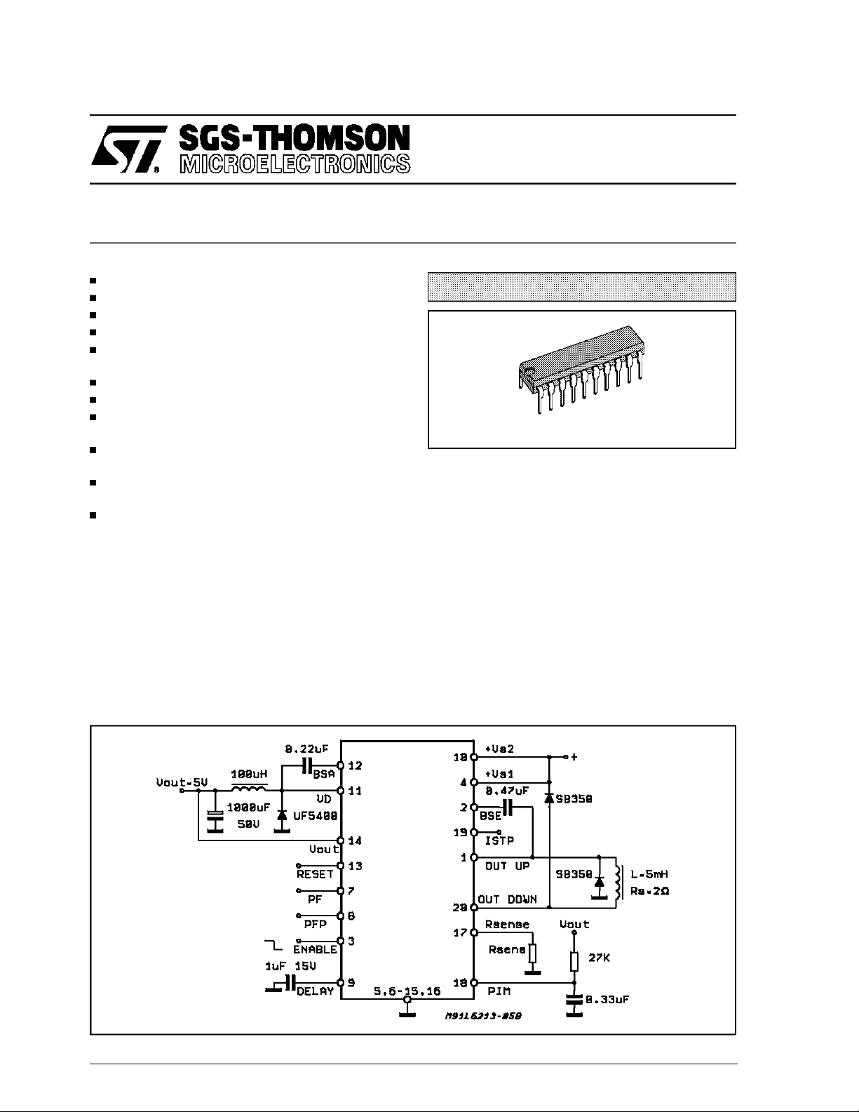
The L6213 is an IC containing a S.M.P.S. delivering 1A at a voltage of 5V and a section designed
to drive a solenoidwithacurrent up to5A.
The device is realized in BCD mixed technology,
which combines isolated DMOS power transistor
with CMOSand Bipolar circuitson the samechip.
The SMPSsection can deliver 1A DC with anout-
APPLICATIONCIRCUIT
DS ON
FOR HIGH SIDE
MULTIPOWERBCD TECHNOLOGY
Powerdip 16+2+2
put voltage of 5V, including current limiting, reset
and power fail for microprocessor and thermal
protection.
The solenoid driver section is designed for high
current applications like hammer driver in electronictypewriter.
Thesolenoidoutputsectioncontainsa high sideand
a low side DMOS, which R
high si de chopping.The current rising slopeisexternallyprogra mmabl ethroughanexternalcapacitor .
The level of hysteresis of the current can be
changedthroughan externalresistor.
The device is supplied in Powerdip 16+2+2, and
use the four center pins to conduct heat to the
printedcircuit.
are optimized for
DS ON
November 1991
This isadvanced information on anew product now in development or undergoing evaluation.Details are subject to change without notice.
1/9
Page 2
L6213
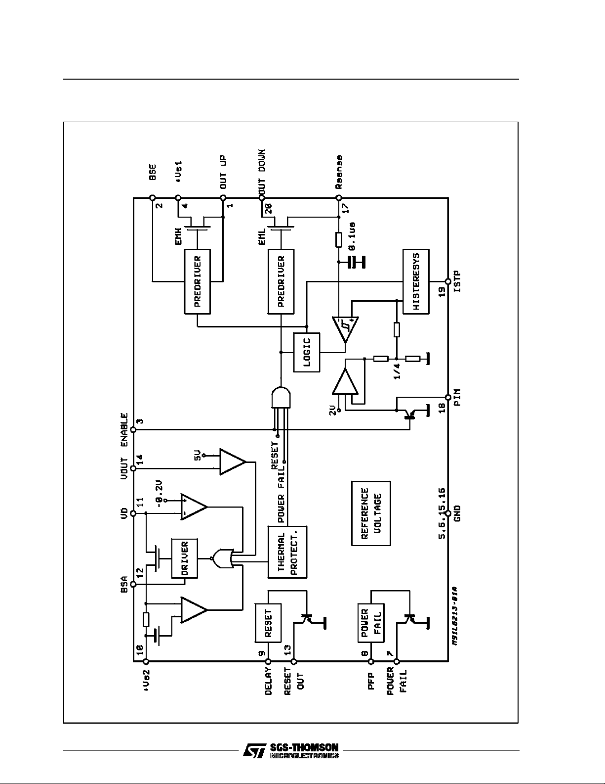
BLOCK DIAGRAM
2/9
Page 3
ABSOLUTE MAXIMUMRATINGS
Symbol Parameter Value Unit
V
V
D;VOUT-UP
V
V
OUT-DOWN
V
OUT-UP
PFP Input Voltage 25 V
, Enable
V
O
PIM
Reset, PF Output Voltage 20 V
CD, ISTP Input Voltage 5.5 V
Out-Up
Out-Down
T
stg
Supply Voltage 52 V
S
Output Negative Voltage DC -1.3 V
Output Negative Voltage peak at t= 0.1µs f = 100KHz -5V V
D
Output Positive Voltage DC VS+ 1.3 V
Output Positive Voltage peak at t = 0.1µs f = 25KHz V
+5 V
S
Output Negative Voltage peak at t= 0.1µs f = 25KHz -5 V
Input Voltage 7 V
Output Current DC = 10% T
= 3.5ms 5.5 A
ON
Storage Temperature -50 to 150 °C
L6213
THERMAL DATA
Symbol Description Value Unit
R
th j-pins
R
th j-amb
Thermal Resistance Junction-pins
Thermal Resistance Junction-ambient
Max.
Max.
14
60
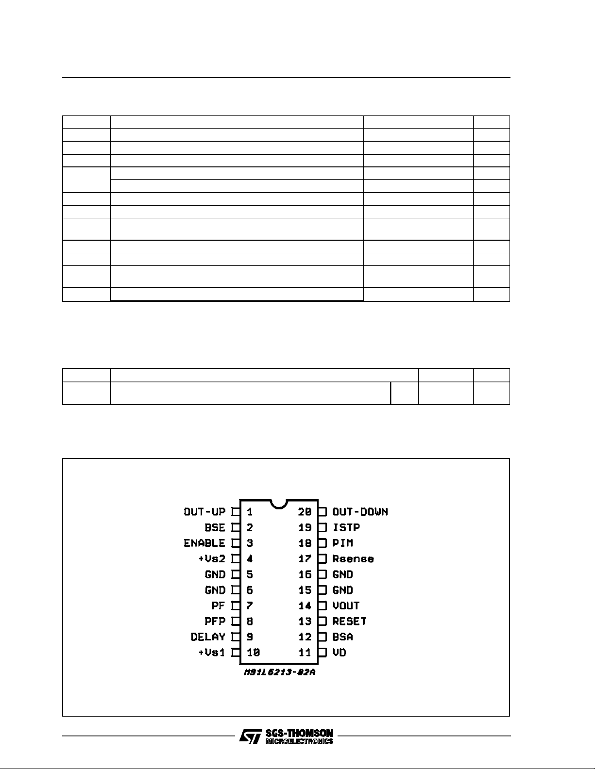
PIN CONNECTION (Top view)
°C/W
°C/W
3/9
Page 4

L6213
PIN DESCRIPTION
Nr. Name Description
1 Out-Up Solenoid section upper DMOS output.
2 BSE Solenoid section upper DMOS bootstrap. A capacitor connected between pin 2 and pin 1
3 ENABLE Solenoid control input - TTL compatible.
4+V
S1
5, 6 GND Ground.
7 PF Power fail output, the saturation of PF isguaranteed if VPS exceed 3V. PF is at logic1 a
8 PFP Power fail programming. A resistor divider connected to VPS changesthe Power fail
9 CD Capacitor delay. A capacitor connected to this pin determines theReset signal delay time
10 V
S2
11 VD Regulator output and diode voltage control.
12 BSA SMPS section DMOS bootstrap. A capacitorconnected between pin 12 and pin 11
13 RESET Reset output. The saturation of Reset is guaranteedif VPSexceeds 3V. The Reset output
14 V
out
15, 16 GND Ground.
17 R
sense
18 PIM Programming of solenoid current rising edge. An RC network connected to this pin
19 ISTP Programming of solenoidcurrent histeresys.
20 Out-Down Solenoid section lower DMOS output.
ensures the efficientdriving of the solenoid section upper DMOS.
Unregulated voltage input -Solenoid section.
time T
after RESET reachedthe high level. PF came back to logic 0when VPS goes
1
down under 18V. (see fig. 1)
threshold levels.
t
.
d
Unregulated voltage input -SMPS sections.
ensures efficient driving of SMPS DMOS.
reaches the logic level 1 a time delay (set by capacitorCD) afterVPS has reached a
rising threshold voltage. Reset reaches 0 level when VPS goes down below folling
threshold.
Feed back input of theregulation loop.
Connection for solenoid sensing resistor.
determines the slope of the solenoid current rising edge.
ELECTRICAL CHARACTERISTICS (Refer to the application circuit, TJ=25°C, I
Power Supply =
out
50mA,VPSfrom 12V to 46V; unless otherwisespecified.
Pin Symbol Parameter Test Condition Min. Typ. Max. Unit
STEP-DOWNSECTION
10, 4 V
14 V
10 t
10 t
10 I
11 I
2, 10 I
2, 10 I
11 t
4/9
R
DS on
hon
h off
lim
dp
t
off
Supply Voltage 14 46 V
i
Output Voltage IO= 0.05 to 1A 4.85 5.2 V
o
On State Drain Resistance TJ=25°C; VPS = 15 to 46V 0.56 0.7 Ω
Turn-on Threshold VPS Rising Fig. 1 10 12 V
Turn-off Threshold VPS Falling Fig. 1 10 12 V
Input Bias Current 15 mA
B
Static Current Limiting 2.2 3.4 A
Total Input Current ENABLE = 1, VPS = 46V,
i
Total Input Current ENABLE = 1, VPS = 15V,
i
I
I
load
load
=0
=0
Protection CurrentMaximum
Delay Time
Minimum Power off State VPS =46V IO= 50mA 4.2 7.8 µs
13 mA
18 mA
1 µs
Page 5

L6213
ELECTRICALCHARACTERISTICS (continued)
Pin Symbol Parameter Test Condition Min. Typ. Max. Unit
POWERFAIL
10 V
10 V
thR
thF
10 ∆V
8I
8V
8V
8 ∆V
PFI
th-PFP
th-PFP
th -PFP
7V
Rising Threshold Voltage PFP open Fig. 1 19.5 20 23 V
Falling Threshold Voltage PFP open Fig. 1 16.6 18.1 19.5 V
Threshold Hysteresis PFP open Fig. 1 0.5 V
th
Divided InternalCurrent 130 µA
Rising Threshold Voltage VPS = 24V 1.1 1.21 1.29 V
Falling Threshold Voltage VPS = 24V 0.98 1.06 1.13 V
Threshold Hysteresis VPS = 24V 30 mV
Output PF Saturation PF current = 2.5mA
sat
VPS = 3 to 46V
7I
leak
Output Leakage Current VPS = 46V VPF =20V 50 µA
7 t1 Delay to Reset RESET High to PF high
Delay Time (fig. 1)
7 t2 Noise Immunity When VPS drops to 8V for a
time from 0 to t2, PF must be
at 1 logic level (fig.2)
7 t3 Noise Immunity When VPS drops to 17V for
a time greater than t3,PF
must be at 0 logic level (fig. 2)
RESET
9I
9I
13 V
13 I
leak
13 t4 Noise Immunity When VPS drops to 10V for a
Delay Source Current VD= 0 to 4.1V 70 140 µA
d
Delay Sink Current VD = 4.3 to 2V 10 mA
d
Output RESET Saturation RESET Current = 2.5mA
sat
VPS = 3 to 46V
Output Leakage Current VPS = 46V RD = 4 to 5V
V
= 20V
RESET
timegreater thant4 RESET
must be at 0logic level(fig. 1)
SOLENOIDCONTROLSECTION
0.4 V
01µs
01µs
4 µs
0.4 V
50 µA
4 µs
18 Vsat Saturation Voltage ENABLE = 1 I PIM = 5mA 0.2 V
18 I
18 V
leak
clamp
17 Minimum Offset Threshold PIM = GND V
Leakage Current PIM= 0.2to 2.5VENABLE= 0 +100 µA
Clamp Voltage 1.9 2 2.1 V
sens
= 10mV
lower MOS must be in conduction
ENABLE = 0
17 MAximum Offset Voltage PIM = GND V
sens
= 50mV
lower MOS must be open
ENABLE = 0
17 V
sense
Static Voltage Limiting
Threshold
V
going from 0to 0.6V
sens
PIM = 3V, the EMH DMOS
0.475 0.5 0.525 V
goes to high resistance state
when V
is within:(see
sens
Block Diagram)
17 Maximum Delay Time 1 µs
EMH R
EML R
17 V
t
sense
Protection Time 2 4 µs
p
OnSta teDr a in toSo urceR esi stan c e Tj=25°C, VPS 15 to 46V 0.35 0.45 Ω
on
OnStateDrai nto SourceResista nce Tj = 25°C, VPS 15 to 46V 0.28 0.4 Ω
on
Vsense Hysteresis IST = Open
IST = 0.75V
IST = 3V
35
15
80
50
25
100
65
35
120
mV
mV
mV
5/9
Page 6

L6213
Figure1: PowerFail and Reset Static Operation.(PFP open)
6/9
Page 7

Figure2: PowerFail and Reset Noise Immunity and Dynamic Operation.
L6213
7/9
Page 8

L6213
POWERDIP20 PACKAGEMECHANICAL DATA
DIM.
MIN. TYP. MAX. MIN. TYP. MAX.
a1 0.51 0.020
B 0.85 1.40 0.033 0.055
b 0.50 0.020
b1 0.38 0.50 0.015 0.020
D 24.80 0.976
E 8.80 0.346
e 2.54 0.100
e3 22.86 0.900
F 7.10 0.280
I 5.10 0.201
L 3.30 0.130
Z 1.27 0.050
mm inch
8/9
Page 9

L6213
Information furnished is believed to be accurate and reliable. However, SGS-THOMSON Microelectronics assumes no responsibility for the
consequences of use of such informationnor for any infringement ofpatents or other rights of third parties which may result from itsuse. No
license is granted by implication or otherwise under any patent or patent rights of SGS-THOMSON Microelectronics. Specifications mentioned in this publication are subject to change without notice. This publication supersedesand replaces all information previously supplied.
SGS-THOMSON Microelectronics products are not authorized for use as critical components in life support devices or systems without express written approval of SGS-THOMSON Microelectronics.
1994 SGS-THOMSON Microelectronics - All RightsReserved
SGS-THOMSON Microelectronics GROUPOF COMPANIES
Australia - Brazil - France - Germany - Hong Kong - Italy - Japan- Korea -Malaysia -Malta - Morocco - The Netherlands- Singapore -
Spain - Sweden - Switzerland - Taiwan- Thaliand - United Kingdom - U.S.A.
9/9
 Loading...