

Page 1
®
VOLTAGE REG ULAT O R FOR CA R RA DI O
5 REGULATORS
10V (350mA); 8.5V (175mA); 5V (350mA); 5V
(250mA); 8V/10V (1A)
ALL REGULATORS ARE LOW DROPOUT
OUPUTS
3 HIGH SIDE DRIVER S:
2A (HSD1), 0.45A (HSD2 & HSD3)
NO EXTERNAL CHARGE PUMP CAPACITORS ARE REQUIRED
STAND BY MODE CONTROLLED BY 3 INPUT PIN S:
ENABLE FOR REG2 AND REG 3,
2
I
C BUS FOR REG1, REG4, REG5, HSD1,
HSD2, HSD3
INDIVIDUAL THERM AL SHUT DOW N
INDEPENDENT CURRENT LIMITING
SHORT CIRCUIT PROTECTION
LOAD DUMP PROTECTION AND OVERVOL-
TAGE SHUTDOWN
ESD PROTECTED
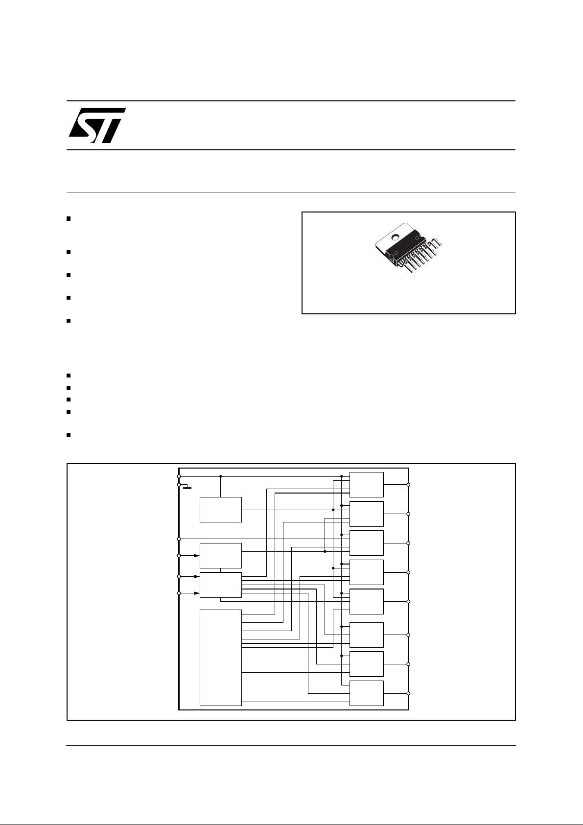
L5950
MULTIPLE MULTIFUNCTION
Multiwatt15
DESCRIPTION
The ASPM (Audio System Power Module) is an
integration of three high side drivers and five
regulators developed to provide the power for an
audio system.
The outputs of the IC are controlled via the I
bus and the Enable input.
External protection must be provided for reverse
battery protection.
2
C
BLOCK DIAGRAM
BAT
GND
VREF
ENABLE
SCL
SDA
VOLTAGE
REFERENCE
8.5 & 5V
ENABLE
PC OUTPUT
CONTROL
CURRENT
LIMIT
PROTECTION
LOGIC
INDIVIDUAL
THERMAL
SHUTDOWN
OVERVOLTAGE
PROTECTION
REG 1
10V 350mA
REG 2
8.5V 175mA
REG 3
5V 350mA
REG 4
8V/10V 1A
REG 5
5V 250mA
DRIVE 1
2A
DRIVE 2
450mA
DRIVE 3
450mA
REG1
REG2
REG3
REG4
REG5
HSD1
HSD2
HSD3
D99AU1002
March 2001
1/8
Page 2
L5950
ABSOLUTE MAXIMUM RATINGS
Symbol Parameter Value Unit
V
S
V
S
V
in
V
out
T
op
T
stg
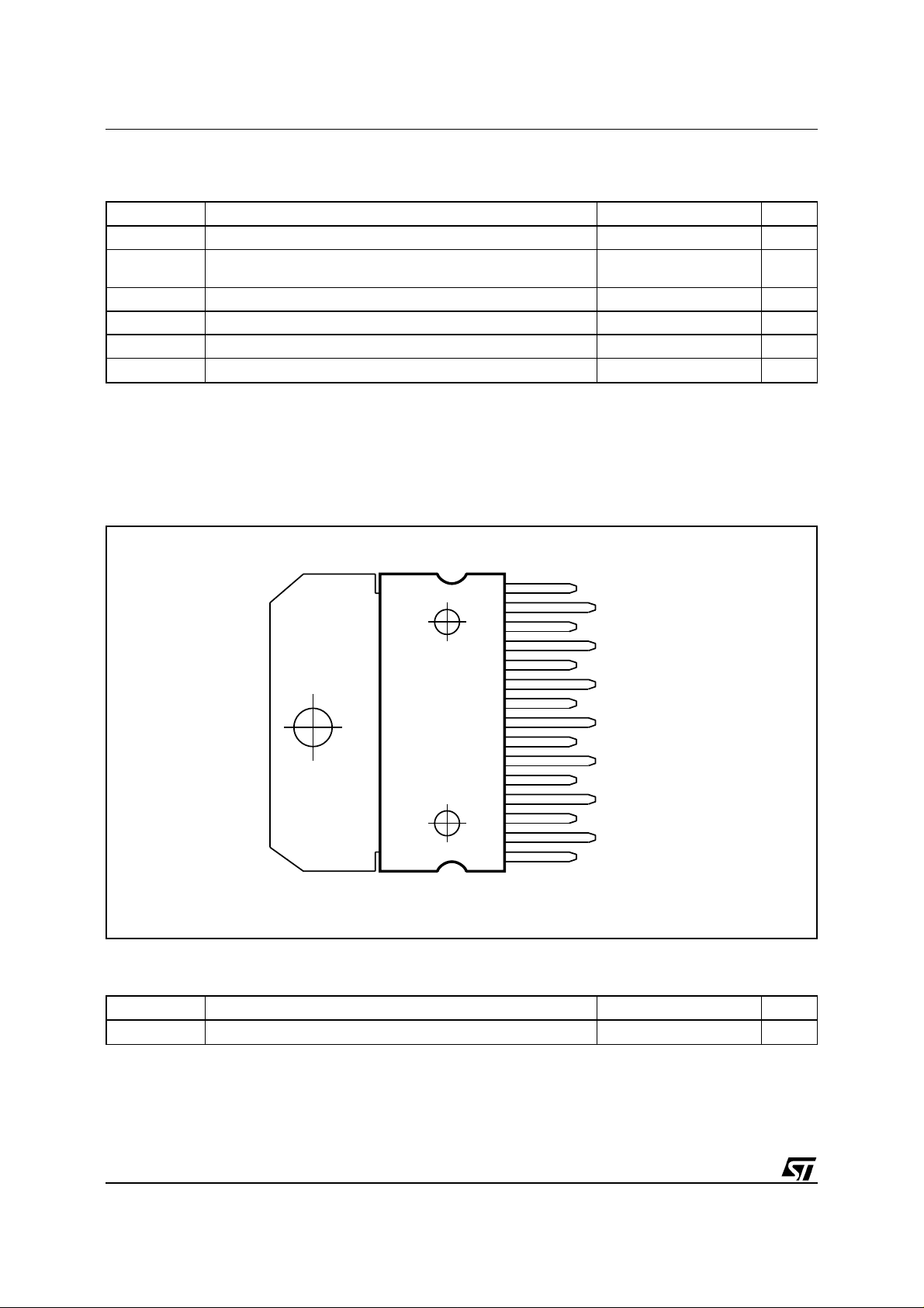
PIN CONNECTION
DC Operating Supply Voltage -0.6 to 26.5 V
Transient Supply Overvoltages, rise time = 10ms
34 V
delay time = 115ms
Input Voltages (EN, SDA, SCL) -0.6 to 9 V
Output Control Voltage -0.6 to 6.0 V
Operating Temperature Range -40 to 85
Storage Temperature Range -40 to 150
C
°
C
°
15
14
13
12
11
10
9
8
7
6
5
4
3
2
1
REG4
BAT
REG5
REG3
REG2
REG1
VREF
GND
SCL
Enable
SDA
HSD3
HSD2
BAT
HSD1
D99AU1006
THERMAL D AT A
Symbol Parameter Value Unit
Rth j-case Thermal Resistance Junction-case 2 °C/W
2/8
Page 3
L5950
ELECTRICAL CHARACTERISTICS
(Refer to the application circuit, V
= 14.4V; T
S
= 25°C; unless
amb
otherwise specified.)
Symbol Parameter Test Condition Min. Typ. Max. Unit
I
q,ST-BY
I
q
I
EN
, V
V
IL
10V/350mA REG 1 OUTPUT
V
REG1
V
∆
line
V
∆
load
V
DROPOUT
I
lim1
SVR Ripple Rejection f
8.5V/175mA REG 2 OUTPUT
V
REG2
V
∆
line
V
∆
load
V
DROPOUT
I
lim2
SVR Ripple Rejection f
5V/350mA REG 3 OUTPUT
V
REG3
V
∆
line
V
∆
load
Standby Quiescent Current All Outputs Off, V
Maximum Quiescent Current V
Enable Input Current V
BAT
I
REG2
I
REG4
I
HSD1
BAT
= 14V, I
= 175mA, I
= 1A, I
REG5
= 2A, I
HSD2,3
= 14V,
= 14V 2
BAT
= 350mA,
REG1
REG3
= 350mA,
= 250mA,
= 450mA
Enable ≥ 2V
V
BAT
= 14V,
-10
Enable ≥ 0.8V
Enable Threshold Voltage V
IH
Output Voltage I
= 14V, V
BAT
V
= 14V, V
BAT
= 350mA
REG1
11V ≤ V
CC
IL
IH
≤ 16V
2
9.50 10 10.5 V
Line Regulation 11V ≤ VCC ≤ 26V
(Measure ∆ V
REG1
Across V
CC
Range)
Load Regulation 5mA ≤ I
Dropout Voltage (Measure
V
- V
REG1
when V
REG1
BAT
0.1V)
drops
(Measure V
V
REG1
I
REG1
I
REG1
≤ 350mA 55 mV
REG1
- V
REG1
when
BAT
drops 0.1V)
= 350mA
= 5mA
Current Limit 0.51 1.1 A
= 1kHz, V
o
BAT
= 14V
50 dB
with 1Vpp AC
I
= 175mA
REG1
Output Voltage I
Line Regulation 9.5V ≤ V
= 175mA
REG2
9.5V ≤ V
BAT
BAT
(Measure ∆ V
≤ 16V
≤ 26V
REG2
Across V
8.3 8.5 8.7 V
BAT
Range)
Load Regulation 5mA ≤ I
Dropout Voltage (Measure VBAT- V
V
REG2
I
REG2
I
REG2
≤ 175mA 50 mV
REG2
when
REG2
drops 0.1V)
= 175mA
= 5mA
Current Limit 280 525 mA
= 1kHz, V
o
BAT
= 14V
50 dB
with 1Vpp AC
I
= 100mA
REG2
Voltage Offset from VREF 10 40 mV
Line Regulation 7V ≤ V
(Measure ∆ V
BAT
≤ 26V
REG3
Across V
BAT
Range)
Load Regulation 5mA ≤ I
≤ 350mA 100 mV
REG3
150 mA
10
0.8 V
55 mV
900
300
50 mV
900
300
40 mV
µ
µ
µ
V
mV
mV
mV
mV
A
A
A
3/8
Page 4

L5950
ELECTRICAL CHARACTERI S TICS
(continued)
Symbol Parameter Test Condition Min. Typ. Max. Unit
V
DROPOUT
I
lim3
SVR Ripple Rejection f
Dropout Voltage (Measure
VBAT- V
REG3
when V
REG3
drops 0.1V)
(Measure VBAT- V
V
drops 0.1V)
REG3
I
= 175mA
REG3
I
= 5mA
REG3
REG3
when
950
600
Current Limit 0.5 1 A
= 1kHz, V
o
BAT
= 14V
50 dB
with 1Vpp AC
I
= 175mA
REG3
8/10V/1A REG 4 OUTPUT
V
∆
REG4
V
line
Output Voltage I
REG4
= 1A
b5 = 0
b5 = 1
Line Regulation 11V ≤ V
(Measure ∆ V
≤ 26V, b5 = 1
BAT
REG2
Across V
BAT
7.6
9.50
10
8
8.4
10.5
50 mV
Range)
V
∆
V
DROPOUT
I
lim4
load
Load Regulation 5mA ≤ I
Dropout Voltage (Measure VBAT- V
Current Limit 1.3 2.4 A
SVR Ripple Rejection f
V
REG2
I
REG4
I
REG4
= 1kHz, V
o
≤ 1A 150 mV
REG4
when
REG2
drops 0.1V)
= 1A
= 5mA
BAT
= 14V
50 dB
950
600
with 1Vpp AC
I
= 500mA
REG4
5V/250mA REG 5 OUTPUT
V
∆
REG5
V
line
Output Voltage I
REG5
Line Regulation 7V ≤ V
(Measure ∆ V
= 250mA 4.75 5 5.25 V
BAT
≤ 26V
REG5
Across V
BAT
40 mV
Range)
V
∆
V
DROPOUT
I
lim5
load
Load Regulation 5mA ≤ I
Dropout Voltage (Measure VBAT- V
Current Limit 320 700 mA
SVR Ripple Rejection f
V
REG5
I
REG5
I
REG5
= 1kHz, V
o
≤250mA 100 mV
REG5
when
REG5
drops 0.1V)
= 250A
= 5mA
BAT
= 14V
50 dB
1.6
1.2
with 1Vpp AC
I
= 125mA
REG5
2A HSD1
V
sat
Output Saturation Voltage IHSD1 = 1A
0.5 V
Continuous Time Operation
I
leak1
I
lim
Output Leakage Current All Driver Outputs are Off -50 50
Current Limiting R
HSD1
= 0.5
Ω
2.4 4 A
0.45A HSD2 & HSD3
V
sat
Output Saturation Voltage IHSD2,3 = 300mA
0.6 V
Continuous Time Operation
I
leak2,3
I
lim
Output Leakage Current All Driver Outputs are Off -50 50
Current Limiting R
HSD2,3
= 0.5
Ω
0.56 1 A
mV
mV
V
V
mV
mV
V
V
µ
µ
A
A
4/8
Page 5

L5950
ELECTRICAL CHARACTERI S TICS
(continued)
Symbol Parameter Test Condition Min. Typ. Max. Unit
2
CHARACTERISTICS FOR I
V
IL
V
IH
V
HYS
V
OL1
V
OL2
I
I
f
SCL
LOW Level Input Voltage 1.5 V
HIGH Level Input Voltage 3 V
Input Hysteresis 0.2 V
LOW Level Output Sink Current = 3mA
Input Current 0.4V ≤ VI ≤ 0.9V
SCL Clock Frequency 400 kHz
FUNCTIONAL DESCRIP TION
The three high side drivers are a 2.0A output
(HSD1), and two 450mA outputs (HSD2 & 3). The
five regulator outputs are a 10V at 350mA
(REG1), an 8.5V at 175mA (REG2), a 5V at
350mA (REG3), an 8V/10V at 1A (REG4), and 5V
at 250mA (REG5). The regulators are low dropout. The regulators will operate with output capacitors with ESR of 0.1Ω to 5Ω.
The 8.5V regulator output (REG2) is a tighter tolerance output than the other regulator outputs.
The 8.5V output is a ±2.5% (5% total range) output over temperature. This is required on the
regulator to improve performance and reduce
cost on the 8.5V driven IC’s in the radio. The
tighter tolerance is possible by performing a trim
of the bandgap reference to the 8.5V output. The
other outputs are ±5% variation over temperature.
C
0.4
Sink Current = 6mA
DDmax
-10 10
0.6
while 10V is the output voltage when bit5 = ’1’.
When all outputs are turned off the total current
draw must be minimized. I
2
C will run at a clock
speed range of 100kHz to 400kHz. This device
should be capable of operating at any frequency
within this range.
Protection
The L5950 can survive under the following conditions: shorting the outputs to BAT and GND, loss
of BAT, loss of IC GND, double battery(+26.5V),
4000V ESD, 34V load dump. L5950 will not handle a reverse battery condition. External components must be implemented for reverse battery
protection.
Thermal Shutdown: REG1, REG2, REG3, REG4,
REG5 outputs shutdown at 160°C and return to
normal operation at 130°C. The HSD2 and HSD3
shutdown at 160°C and return to normal operation at 130°C. The HSD1 with go into thermal
REG3 is referenced from the VREF input not the
internal bandgap. This is done to minimize the
voltage offset between individual 5V supplies.
The REG2 and REG3 outputs are turned on and
off with the Enable input, a ’1’ turns the outputs on
and a ’0’ turns them off. When Enable is "1", the
other outputs can be independently controlled via
2
C bus. When a given regulator is turned off it
the I
must be guaranteed to be lower than 0.2V. The
output voltage of REG4 is selected via bit 5 of the
2
C data byte: 8V is the output voltage if bit5 = ’0’
I
shutdown at 170°C and returns to operation at
120°C.
Current Limiting: each voltage regulator will contain its own current protection.
Short Circuit: If the outputs are short circuited, the
IC will go into current limiting and eventually the
thermal shutdown will kick in. Current limiting will
not disable the outputs.
Overvoltage: The IC will not operate if the BAT
voltage reaches 27V typ. or above.
V
V
A
µ
Figure 1. Definition of Timing on the I2C Bus.
SDA
t
BUP
SCL
PS P
t
HD;DAT
t
LOW
t
HD;DAT
t
R
t
HIGH
t
F
t
SU;DAT
t
SU;STA
t
HD;STA
Sr
D99AU1007
t
SP
t
SU;STO
5/8
Page 6

L5950
Figure 2. Typical Application Circuit.
EN
FBATT
1000µF0.1µF
(*) ESR of output capacitors should be between 0.1Ω and 5.0Ω.
VREF
ENABLE
BAT
VREF
SCL
SDA
GND
REG1
REG2
REG3
REG4
REG5
HSD1
HSD2
HSD3
REG5
C14
10µF
REG4
C12
10µF
HSD1
HSD2
HSD3
D99AU1010A
REG3
C10
10µF
REG2
C8
10µF
REG1
C6
10µF
WRITE MODE:
CHIP ADDRESS DATA BYTE
S 0 A A .. .. P
MSB LSB MSB LSB
S = START condition - SDA goes from high to low while SCL is high
A = Acknowledge - the device being written to, pulls down on data line (SDA) during the acknowledge
clock pulse.
P = STOP condition - SDA goes from low to high while SCL is high.
CHIP ADDRESS BYTE:
CHIP ADDRESS READ/WRITE
A7 A6 A5 A4 A3 A2 A1 A0
00010000
DATA BYTE:
DATA BYTE
REG1 R4 10V REG4 REG5 HSD1 HSD2 HSD3
b7 b6 b5 b4 b3 b2 b1 b0
X
Default mode is 0000 0000 which corresponds to all outputs being off, low power mode.
Bit 5 Controls the output voltage of REG4. A ’0’ corresponds to 8V and a ’1’ corresponds to 10V.
6/8
Page 7

L5950
DIM.
MIN. TYP. MAX. MIN. TYP. MAX.
A 5 0.197
B 2.65 0.104
C 1.6 0.063
D 1 0.039
E 0.49 0.55 0 .019 0.022
F 0.66 0.75 0.026 0.030
G 1.02 1.27 1.52 0.040 0.050 0.060
G1 17.53 17.78 18.03 0.690 0.700 0.710
H1 19.6 0.772
H2 20.2 0.795
L 21.9 22.2 22.5 0.862 0.874 0.886
L1 21.7 22.1 22.5 0 .854 0.870 0.886
L2 17.65 18.1 0.695 0.713
L3 17.25 17.5 1 7.75 0.679 0.689 0.699
L4 10.3 10.7 10.9 0 .406 0.421 0.429
L7 2.65 2.9 0.104 0.114
M 4.25 4.55 4.85 0.167 0.179 0.191
M1 4.63 5.08 5.53 0.182 0.200 0.218
S 1.9 2.6 0.075 0.102
S1 1.9 2.6 0.075 0.102
Dia1 3.65 3.85 0.144 0.152
mm inch
OUTLINE AND
MECHANICAL DATA
Multiwatt15 V
7/8
Page 8

L5950
Information furnished is believed to be accurate and r el i abl e. H owever, STMicroelec tronics assumes no responsibility for the consequences
of use of such informatio n nor for any infringement of patents or other ri ghts of third parties which may res ult from its use. No license is
granted by im plicat ion or ot herw ise under any patent or pat ent right s of ST Micro electronics . Speci fication ment ioned in this publication are
subject to c hange without notice. This publication supers edes and replaces al l information previously supplied. STMicroelectron i cs products
are not authorized for use as critical components in life support devices or systems without express written approval of STMicroelectronics.
The ST logo is a registered trademark of STMicroelect roni cs
© 2001 STMicroelectronics – Printed in Italy – All Rights Reserved
STMicroelectronics GROUP OF COMPANIES
Australia - Brazil - China - Finland - France - Germany - Hong Kong - India - Italy - Japan - Malaysia - Malta - Morocco -
Singapore - Spain - Sweden - Switzerland - United Kingdom - U.S.A.
http://www.st.com
8/8
 Loading...