

Page 1
MULTIFUNCTIONINJECTION INTERFACE
.DRIVES ONE OR TWO EXTERNAL DAR-
LINGTONS
.DUAL AND SINGLE LEVEL CURRENT CON-
TROL
.SWITCHMODECURRENTREGULATION
.ADJUSTABLEHIGHLEVELCURRENT DURA-
TION
.WIDE SUPPLYRANGE(4.75 - 46V)
.TTL-COMPATIBLELOGICINPUTS
.THERMAL PROTECTION
.DUMP PROTECTION
DESCRIP TIO N
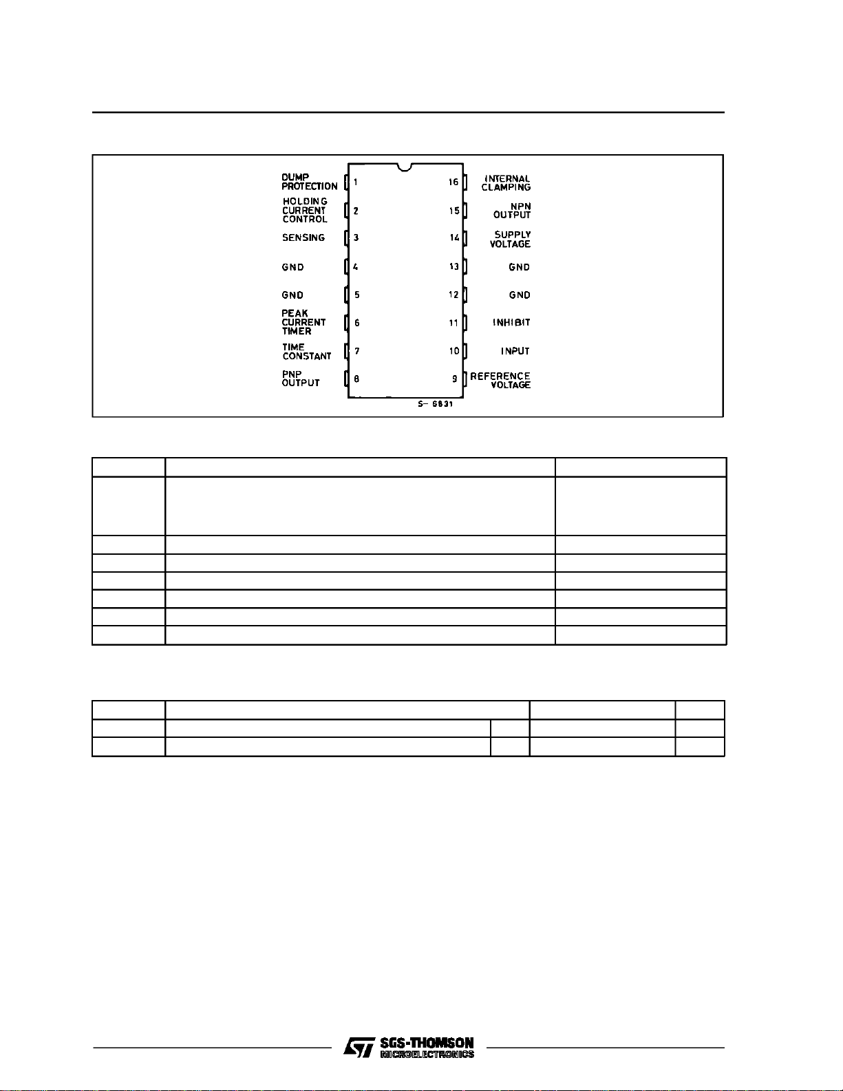
TheL584 is designedto drive injectorsolenoidsin
electronic fuel injection systems and generally inductiveloads for automotive applications.The device is controlled by two logic inputs and features
switchmoderegulationoftheloadcurrentdrivingan
externaldarlingtonandan auxiliaryonefor the current recirculation.A key featureof the L584is flexibility. It canbe used with a varietyof darlingtonsto
match the requirements of the load and it allows
bothsimpleandtwolevelcurrentcontrol.Moreover,
L584
PRELI MINA RY DATA
DIP16 (12+2+2)
ORDERING NUMBER : L584
the drive waveshape can be adjusted by external
components.Other features of the device include
dump protection,thermal shutdown, a supply voltagerangeof4.75-46VandTTL-compatibleinputs.
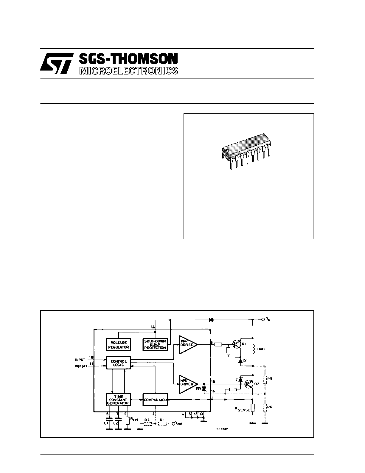
TheL584is suppliedin a16leadPowerdippackage
whichuses the four center pins to conduct heat to
the PC board copper.
BLOCK DIAG RAM
November 1988
1/13
Page 2
L584
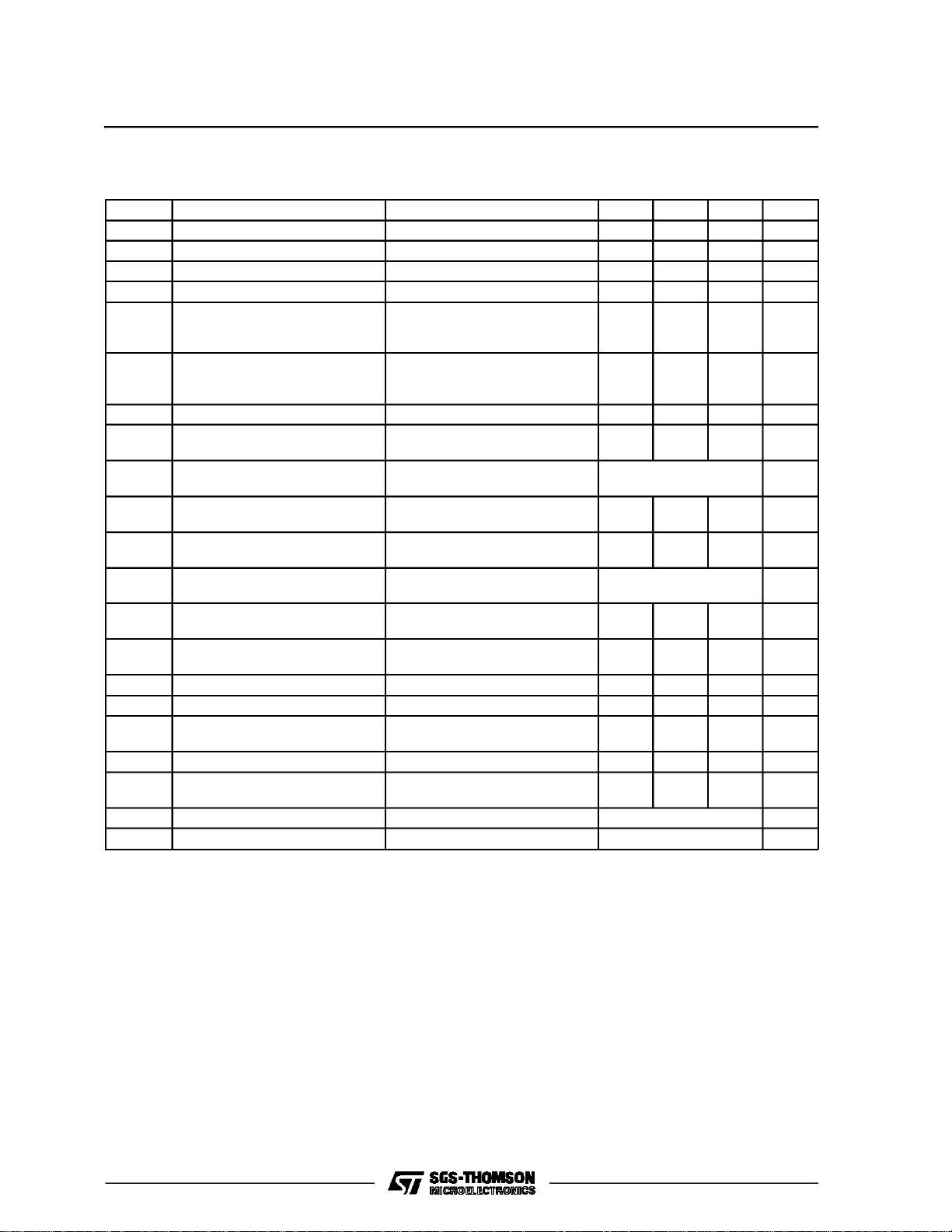
PIN CO NNEC TIO N
ABSOLUTE MAXIMUMRATINGS
Symbol Parameter Value
V
V
V
V
sens
V
I
Tstg,Tj Storageand Junction Temperature Range –55 to 150°C
DC Supply Voltage (pin 1 open)
S
– 0.2Vmin; +50V Max
PositiveTransient Voltage
(pin 1 connected to V
(5ms ≤ t
Input Voltage(pins 10, 11) – 0.2V min;+7V Max
1
ExternalReference Voltage (pin 2) – 0.2V min;+7V Max
r
≤ 10ms,R
rise
, πffalltime constant = 100ms)
S
≥ 0.5Ω)
source
SenseVoltage (pin 3) – 0.2V min;+7V Max
Max D.C. and Transient Voltage 50V
8
ReferenceCurrent (pin 9) 5mA Max
r
+60VMax
THERMAL DATA
Symbol Parameter Value Unit
R
th j-pins
R
th j-amb
* Obtained with the GND pins soldered to printed circuitwith minimized copper area.
2/13
ThermalResistance Junction-pins Max. 15 °C/W
ThermalResistance Junction-ambient Max. 80 °C/W
Page 3

PIN FUNCTIONS
o
N
Name Functions
1 Dump Protection With pin 1 connected to pin 14 the device is protectedagainst dump voltage ≤ 60V.
Theprotectio.n operates at V
≥ 32V(typ.).If this protectionis notused thepin must
S
beleft open
2 HoldingCurrent Control Thevoltage V
appliedto this pin sets the holding current level.
set
3 Sensing Connection for load current sense resistor. Vazlue sets thepeak and holding current
levels. I
=0.45/RS(typ.);Ih=V
P
. (see block diagram and fig. 4).
set/Rs
4 Ground Ground Connection. With pins 5, 12 and13 conducts heat to pc board copper.
5 Ground See pin 4.
6 PeakCurrent Timer A capacitorconnected between this pin andgroundsets the duration of the high level
current(t
7 Discharge Time Constant A capacitor connected between this pin and ground sets the duration of t
infig. 4)
2
off
grounded, the current switchmode control is suppressed.
8 PNP DrivingOutput Current sink for external PNPdarlington (for recirculation). I
= 35 Ir (typ).
dp
9 ReferenceVoltage A resistorconnected between this pin and ground setsthe internal current reference,
I
. The recommended value is 1.2kΩ givingIr = 1mA (typ.).
r
10 Input TTL-compatible Input. A highlevel on this pin activatesthe output, drivingthe load.
11 Inhibit TTL-compatible Inhibit Input.A high level on this input disablesthe output stagesand
logic circutry, irrespectiveof the state of pin 10.
12,13 Ground See Pin 4.
14 Supply Voltage Supply Voltage Input.
15 NPN Driving Output Current Source for ExternalNPN Darlington (load driver).I
=100 Ir(typ.)
dn
16 Internal Clamping Internal Clamp Zener for Fast Turn-off.
000
L584
(fig.4). If
3/13
Page 4
L584
ELECTRICAL CHARACTERISTICS (Vs(Pin 14) = 14.4V; –40 ≤ Tj ≤ 105°C; R
= 1.20KΩ unless
ref
otherwise specified; refer to fig. 1)
Symbol Parameter Test Condiction Min. Typ. Max. Unit
OperatingSupply Voltage Pin1 Open 4.75 44 V
V
S
V
V
V
R
I
V
I
V
R
I
V
6SAT
I
V
7SAT
V
V
V
I
V
I
dn
I
dp
Dump ProtectionThreshold Pin 1 = V
d
Dump ProtectionInput Resistance Pin 1 to GND 18 50 kΩ
d
QuiescentCurrent Pin 14 45 mA
q
Input Threshold Voltages Pin10, 11
i
S
Low
High 2.0
Input Current Pin 10, 11
i
Low
High
ReferenceVoltage Pin 9 1.15 1.35 V
r
ReferenceResistor Range Pin 9 to GND
r
PeakDuration ControlCurrent Pin 6
6
PeakDuration Control
6th
I
r=Vr/Rr
V
≤ 1.8V
pin6
Pin 6 1.20 1.6 V
Comparator Threshold
Pin6 SaturationVoltage Pin 6
(dischargestate)
Off DurationControl Current Pin 7
7
Off DurationControl
7th
V
≤ 1.8V
pin7
Pin 7 1.20 1.6 V
Comparator Threshold
Pin7 SaturationVoltage Pin 7
(dischargestate)
PeakCurrent Threshold Voltage Pin 3 400 500 mV
spt
Holding Current SetVoltage Range Pin 2 0 2 V
set
Holding Current SetVoltage Range Pin 3, Peak Value, dV/dt ≤ 1V/
set
Pin3 Bias Current V
3
Recirculation Zener Clamping
cl
= 600mV –200 µA
pin3
Pin16to Pin15@200mAintoPin16 13.5 18.5 V
s
Voltage
NPN Driver Source Current V
=0V 70xIr| 140 x I
pin15
PNP Driver Sink Current Vpin 8 ≥ 4.75V 25 x Ir|60xI
28 36 V
0.8 V
–100
–250
1 3.3 kΩ
/9.50 | Ir/6.00
I
r
|
200 mV
(I
r min
)/9.50 | (I
r max
)/6.00
|
200 mV
V
set
0.01
–
V
set
0.01
+
r
r
V
µA
µA
A
A
V
A
A
4/13
Page 5

APP LICATION INF ORMATION
Controlledby alogicinputand an inhibitinput (both
TTL compatible),thedevicedrivestheexternaldarlington(s) to produce a load current waveform as
shownin figure4. Thisbasicwaveform showsthat
thedeviceproducesaninitialhighlevelcurrentinorder to ensurea fastopening,followedby a holding
level current as long as the input is active. Both
the peak and holdingcurrent are regulatedby the
L584’sswitchmodecircuitry.
Thedurationof thehighlevelcurrentandthe values
ofthepeakandtheholdingcurrentscanbeadjusted
by externalcomponents.
Moreover,by omitting C1, C2 or bothit is possible
to realize single-level current control, a transitory
peak followed by a regulated holding current or a
simple peak (figure1).
Thepeakandholdingcurrentvaluesare alwaysre-
Figure1 : ComponentsConnectedto Pins 6 and 7 Determinethe LoadCurrent Waveshape.
L584
COMPONENTS ON PINS 6 AND 7
LOAD CURRENT WAVEFORM
5/13
Page 6

L584
ferred,inthe followingformula,toIE, emittercurrent
of the external darlingtonQ2,
I
E=ILOAD+Idn
becausethe sensingdetectionis on the darlington
emitter(not directlyon theload).
The peak currentlevel I
sistor,R
, and is found from :
s
I
=0.45 /Rs(typ)
p
The peak valueof holdingcurrentlevel,I
a voltage(V
)appliedto pin2, giving :
set
I
hp=Vsetth/Rs
, is set by the sensingre-
p
, is setby
h
=(V
± 10mV)/R
set
s
The peak to hold currentratio is fixed by V
I
=0.45 / V
p/Ihp
V
isfixedby an externalreferenceand a voltage
set
divider(V
V
set=Vext
, R1, R2infig 2) :
ext
* R2 / (R1 + R2)
setth
set
:
Dueto theparticulardarlingtonstoragetimeandthe
devicereactiontimenot very significantdifferences
canbefoundbetweenI
andIhvalues based on the
p
previousformulaand therealvaluesseenin theapplications.
Ifthe holdingcurrentfunctionisnot used,pin 2cannotbeleftfloatingandit mustbeconnectedto GND.
Figure2 : ApplicationCircuit Showing the OptionalComponents.In particularit illustrates howtheholding
currentlevelis adjustedindependentlyofthepeakcurrent(with R1,R2,V
)andhow theinternal
ext
zenerclamp is connected.This circuit producesthe waveformsshownin Fig.4.
Io(A) Q1 Q2
4 BDX54 BDX53
8 BDW94 BDW93
12 BDV64 BDV65
Figure3 : P.C.Board and ComponentsLayout of theCircuit of Fig. 2 (1 : 1 scale).
6/13
Page 7

L584
The drive current for the two darlingtons and the
waveformtime constantsareall definedinturn bya
resistorbetweenpin 9 and ground.
The recommendedvalue for I
is1mA whichis ob-
r
tained with a 1.2KΩ resistor. The darlington drive
currentsare givenby :
PNP : I
The durationof the high current level (t
=35Irtyp. NPN: Idn=100Irtyp.
dp
in fig 4) is
2
set by a capacitor connected between pin 6 and
ground.Thiscapacitor,C1 isrelatedtothe duration,
t
,by:
2
t2=C
The dischargetime constant(t
capacitorC
from:
t
=C2
off
Figure4 : Waveformsof the TypicalApplicationCircuit of Fig. 2.
V
6th–V6sat
1
I
6
betweenpin7 andgroundandis found
2
V
7th–V7sat
⋅
I
7
C
= 12 (typ.)
=12
1
I
ref
infig 4) is set by a
off
C
r
(typ)
I
ref
7/13
Page 8

L584
Figure5 : When pin 6 is grounded,as shownhere, the injector currentis regulatedat a singlelevel.
Io(A) Q1 Q2
4 BDX54 BDX53
8 BDW94 BDW93
10 BDV64 BDV65
Figure6 : In this applicationcircuit, pin 6 is leftopen to givea single peak followedby a regulatedholding
current.
(A) Q1 Q2
I
o
4 BDX54 BDX53
8 BDW94 BDW93
10 BDV64 BDV65
8/13
Page 9

Figure7 : Switchmodecontrol of the current can be suppressedentirelyby leavingpin 6 open and
groundingpin 7. the peak currentis stillcontrolled.
Io(A) Q1 Q2
4 BDX54 BDX53
8 BDW94 BDW93
10 BDV64 BDV65
L584
Figure8 : Applicationscircuitusing only one darlingtonwith a single level of the injector current.
9/13
Page 10

L584
To have a very shortoff time when the L584 input
goes LOW,aninternalzener is availableon pin16.
This zeneris usedwithan externaldivider,R8, R9,
as shown in figure2.Suitable values can be found
from:
≅ 15V + V
V
pin 16
V
≅ V
CQ2
isthevoltageat thecollectorofQ2. V
(V
CQ2
pin 16
BEQ2
R9 + R8
.
+ VRsense
R8
CQ2
max
is 47V if thepin 8 isused forslow recirculationas in
fig. 2).
To ensurestability,a small capacitor(about200pF)
must beconnectedbetweenthe base andcollector
of Q2 when pin 16 is used.
A differentopportunityfor a fastoff timeis basedon
the use of the externalzener diodeDz. In this case
also themaximum Dz voltage valueis 47V.
LOAD DUMP PRO TE CTION
To protectthedeviceagainstthepositiveloaddump
it is necessaryto connect pin 1 to V
ishigherthan32V,the deviceturns offQ2and
if V
S
turnsonQ
. TheexternalresistorR6must be used
1
. In thiscase,
S
(see application circuit) to avoidthat pin 8 voltage
exceeds50V during loaddump. R
V
DUMP–V8
I
dp
where V
4.75V< V
ForthisR
R6>
is the dump voltage value and V8:
DUMP
<47V.
8
value,themini mumsupplyvoltageV
6
mustbe :
6
Smin
guaranteeingQ1 operationis givenby :
V
Smin
In relationto V
Ip
= R6
B
Q1
it isno moreverified Idp=35I
Smin
(+2)
V
BEQ1
R
5
+ V
8sat
ref
(typ) even if the system correct operation is completelyguaranteed.
The L584 application circuit suggested in these
notesallowsthe useofinductiveloadswiththelowestpossibleseriesresistance(compatiblewithconstructionalrequirements)andthereforereducesnotablythe powerdissipation.
For example, an electronic injector driven from
14.4Vwhich draws2.4A has a seriesresistanceof
6Ωanddissipates34.56W.Usingthiscircuita injectorwith a 1Ω seriesresistancecanbe usedandthe
power dissipationis :
P
d=RLIL
whereR
2
+VDIL(1– σ)+V
= resistance of injector= 1Ω
L
V
=drop across diode,VD≅ 1V
D
V
= saturationvoltage of Q2, ≅ 1V
sat
R
= R11 = 185mΩ
S
⋅ ILσ +RSI
sat
2
σ
L
σ = duty cycle =20%
therefore:
Pd ≅ 5.76+1.92 + 0.48+ 0.21 = 8.37W
This given two advantages: the size (and cost) of
the injector is reduced and the drive current is reducedfrom2.4A to about0.4A.
Theapplicationcircuitoffigure9 isverysimilartofigure2 exceptthat itshows the use of two supplies:
onefor thecontrolcircuit,one forthe power stage.
10/13
Page 11

Figure 9 : Applicationcircuitshowinghow two separatesuppliescan be used.
L584
In this applicationit is assumedthat the 5V supply
for L584 is taken from a logic supply, which is already protected,againstload dump transientsand
vol-tagereversal.
Pin 1 must be left open, as shownin fig. 9, if V
L
alwayslowerthan46Vevenduringthe voltagetran-
R
sients.
Note that t
is alsorelated to the requiredcurrent
off
S
ripple∆I on the peak or on the holdingcurrent level
by :
t
=– ln
off
o
I
oRL+Voff
off
– ∆I) RL+V
(I
Where: Ioistheinitialcurrentvaluein OFFcondition
(equalto Ip or IHin accordanceto the currentlevel
considered),
V
OFF=VDIODE+VCEQ1
RLis the series resistance value of the inductanceL :
ThereforeC
canbe dimensioneddirectlyby :
2
Lln(Io–∆I)RL+V
I
C2=
REF
12 R
Notethatt
IoRL+V
L
isthe samefor boththepeakandhold-
off
OFF
OFF
ingcurrent.
is
t
timeis givenby :
on
LV
t
=ln
on
RV
– R(I1 – ∆I)
on
– RI1
on
where: I1 is the final current valuein ONcondition
(equalto I
or IHin accordanceto the current level
p
considered),
R=R
L+RSENSE
Von=VS–VCEsatQ2
If the constanttimes are respectively
LL
>20 t
RR
and > 20 t
off
it ispossibleto considera purelyinductiveloadand
therefore:
∆I ∆I
t
=L ;ton=L
off
V
o
V
on
on
11/13
Page 12

L584
DIP16PACKAGE MECHANICAL DATA
DIM.
MIN. TYP. MAX. MIN. TYP. MAX.
a1 0.51 0.020
B 0.77 1.65 0.030 0.065
b 0.5 0.020
b1 0.25 0.010
D 20 0.787
E 8.5 0.335
e 2.54 0.100
e3 17.78 0.700
F 7.1 0.280
I 5.1 0.201
L 3.3 0.130
Z 1.27 0.050
mm inch
12/13
Page 13

L584
Information furnished is believed to be accurate and reliable. However, SGS-THOMSON Microelectronics assumes no responsibility for
the consequences of use of such information nor for any infringement of patents or other rights of third parties which may result from its
use. No license is granted by implication or otherwise under any patent or patent rights of SGS-THOMSON Microelectronics. Specifications mentioned in this publication are subject to change without notice. This publication supersedes and replaces all information previously supplied. SGS-THOMSON Microelectronics products are not authorized for use as critical components in life support devices or
systems without express written approval of SGS-THOMSON Microelectronics.
1994 SGS-THOMSON Microelectronics - All Rights Reserved
Australia - Brazil - France - Germany - Hong Kong - Italy - Japan - Korea - Malaysia - Malta - Morocco - The Netherlands - Singapore-
SGS-THOMSON Microelectronics GROUP OF COMPANIES
Spain - Sweden - Switzerland - Taiwan - Thaliand - United Kingdom - U.S.A.
13/13
 Loading...