

Page 1
DEVICES INCORPORATED
L4C381
16-bit Cascadable ALU
L4C381
DEVICES INCORPORATED
FEATURES DESCRIPTION
❑❑
❑ High-Speed (15ns), Low Power
❑❑
16-bit Cascadable ALU
❑❑
❑ Implements Add, Subtract, Accumu-
❑❑
late, Two’s Complement, Pass, and
Logic Operations
❑❑
❑ All Registers Have a Bypass Path
❑❑
for Complete Flexibility
❑❑
❑ 68-pin PLCC, J-Lead
❑❑
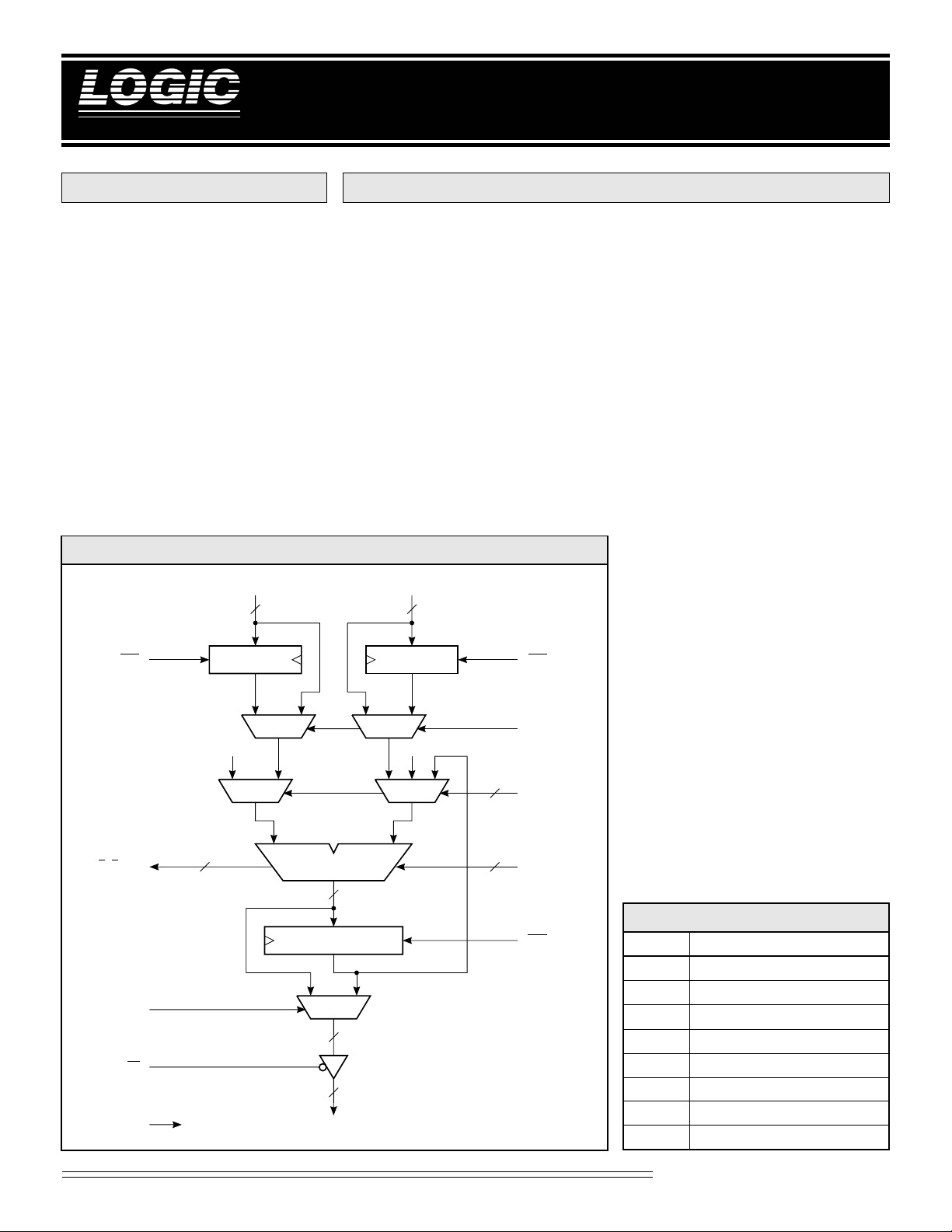
The L4C381 is a flexible, high speed,
cascadable 16-bit Arithmetic and
Logic Unit. It combines four 381-type
4-bit ALUs, a look-ahead carry
generator, and miscellaneous interface
logic — all in a single 68-pin package.
While containing new features to
support high speed pipelined architectures and single 16-bit bus configurations, the L4C381 retains full performance and functional compatibility with
the bipolar ’381 designs.
The L4C381 can be cascaded to
perform 32-bit or greater operations.
See “Cascading the L4C381” toward
L4C381 BLOCK DIAGRAM
B15-B
0
B REGISTER
ENA
A15-A
0
16 16
A REGISTER
16-bit Cascadable ALU
the end of this data sheet for more
information.
ARCHITECTURE
The L4C381 operates on two 16-bit
operands (A and B) and produces a
16-bit result (F). Three select lines
control the ALU and provide 3
arithmetic, 3 logical, and 2 initialization functions. Full ALU status is
provided to support cascading to
longer word lengths. Registers are
provided on both the ALU inputs and
the output, but these may be bypassed
under user control. An internal
feedback path allows the registered
ALU output to be routed to one of the
ALU inputs, accommodating chain
operations and accumulation. Furthermore, the A or B input can be
forced to Zero allowing unary func-
ENB
tions on either operand.
P, G, C
OVF, Z
FTF
OE
CLK
ALU OPERATIONS
FTAB
00
2
OSA
OSB
The S2–S0 lines specify the operation
to be performed. The ALU functions
and their select codes are shown in
Table 1.
The two functions, B minus A and
A minus B, can be achieved by setting
16
ALU
16
45
S
2-S0
, C
0
the carry input of the least significant
slice and selecting codes 001 and 010
respectively.
TABLE 1. ALU FUNCTIONS
ENF
S2-S0 FUNCTION
000 CLEAR (F = 00 • • • 00)
001 NOT(A) + B
010 A + NOT(B)
011 A + B
100 A XOR B
101 A OR B
110 A AND B
111 PRESET (F = 11 • • • 11)
TO ALL REGISTERS
RESULT REGISTER
16
16
F15-F
0
Arithmetic Logic Units
1
08/16/2000–LDS.381-P
Page 2
DEVICES INCORPORATED
L4C381
16-bit Cascadable ALU
ALU STATUS
The ALU provides Overflow and Zero
status bits. Carry, Propagate, and
Generate outputs are also provided
for cascading. These outputs are
defined for the three arithmetic
functions only. The ALU sets the Zero
output when all 16 output bits are
zero. The Generate, Propagate, C16,
and OVF flags for the A + B operation
are defined in Table 2. The status
flags produced for NOT(A) + B and
A + NOT(B) can be found by complementing Ai and Bi respectively in
Table 2.
OPERAND REGISTERS
The L4C381 has two 16-bit wide input registers for operands A and B.
These registers are rising edge triggered by a common clock. The A
register is enabled for input by setting
the ENA control LOW, and the B
register is enabled for input by setting
the ENB control LOW. When either
the ENA control or ENB control is
HIGH, the data in the corresponding
input register will not change.
This architecture allows the L4C381 to
accept arguments from a single 16-bit
data bus. For those applications that
do not require registered inputs, both
the A and B operand registers can be
bypassed with the FTAB control line.
When the FTAB control is asserted
(FTAB = HIGH), data is routed
around the A and B input registers;
however, they continue to function
normally via the ENA and ENB
controls. The contents of the input
registers will again be available to the
ALU if the FTAB control is released.
OUTPUT REGISTER
The output of the ALU drives the
input of a 16-bit register. This risingedge-triggered register is clocked by
the same clock as the input registers.
When the ENF control is LOW, data
from the ALU will be clocked into the
TABLE 2. ALU STATUS FLAGS
Bit Carry Generate = gi =AiBi for i = 0 ... 15
Bit Carry Propagate = pi =Ai + B i for i = 0 ... 15
P 0 =p0
Pi =pi (P i–1 ) for i = 1 ... 15
and
G 0 =g0
Gi=gi + p i (Gi–1 ) for i = 1 ... 15
C i =Gi–1 + Pi–1 (C 0 ) for i = 1 ... 15
then
G = NOT(G15)
P = NOT(P15)
C 16 =G15 + P 15C 0
OVF = C15 XOR C16
output register. By disabling the
output register, intermediate results
can be held while loading new input
operands. Three-state drivers controlled by the OE input allow the
L4C381 to be configured in a single
bidirectional bus system.
The output register can be bypassed
by asserting the FTF control signal
(FTF = HIGH). When the FTF control
is asserted, output data is routed
around the output register, however,
it continues to function normally via
the ENF control. The contents of the
output register will again be available
on the output pins if FTF is released.
With both FTAB and FTF true (HIGH)
the L4C381 is functionally identical to
four cascaded 54S381-type devices.
OPERAND SELECTION
The two operand select lines, OSA and
OSB, control multiplexers that precede
the ALU inputs. These multiplexers
provide an operand force-to-zero
function as well as F register feedback
to the B input. Table 3 shows the
inputs to the ALU as a function of the
operand select inputs. Either the A or
B operands may be forced to zero.
TABLE 3. OPERAND SELECTION
OSB OSA OPERAND B OPERAND A
00 F A
01 0 A
10 B 0
11 B A
When both operand select lines are
low, the L4C381 is configured as a
chain calculation ALU. The registered
ALU output is passed back to the B
input to the ALU. This allows accumulation operations to be performed
by providing new operands via the A
input port. The accumulator can be
preloaded from the A input by setting
OSA true. By forcing the function
select lines to the CLEAR state (000),
the accumulator may be cleared. Note
that this feedback operation is not
affected by the state of the FTF
control. That is, the F outputs of the
L4C381 may be driven directly by the
ALU. The output register continues to
function, however, and provides the
ALU B operand source.
Arithmetic Logic Units
2
08/16/2000–LDS.381-P
Page 3
DEVICES INCORPORATED
L4C381
16-bit Cascadable ALU
MAXIMUM RATINGS
Storage temperature ........................................................................................................... –65°C to +150°C
Operating ambient temperature........................................................................................... –55°C to +125°C
VCC supply voltage with respect to ground............................................................................ –0.5 V to +7.0V
Input signal with respect to ground ........................................................................................ –3.0 V to +7.0 V
Signal applied to high impedance output ............................................................................... –3.0 V to +7.0 V
Output current into low outputs............................................................................................................. 25 mA
Latchup current ............................................................................................................................... > 400 mA
OPERATING CONDITIONS
Active Operation, Commercial 0°C to +70°C 4.75 V ≤ VCC ≤ 5.25 V
Active Operation, Military –55°C to +125°C 4.50 V ≤ VCC ≤ 5.50 V
ELECTRICAL CHARACTERISTICS
Above which useful life may be impaired (Notes 1, 2, 3, 8)
To meet specified electrical and switching characteristics
Mode Temperature Range (Ambient) Supply Voltage
Over Operating Conditions (Note 4)
Symbol Parameter Test Condition Min Typ Max Unit
VOH Output High Voltage VCC = Min., IOH = –2.0 mA 2.4 V
VOL Output Low Voltage VCC = Min., IOL = 8.0 mA 0.5 V
VIH Input High Voltage 2.0 VCC V
VIL Input Low Voltage (Note 3) 0.0 0.8 V
IIX Input Current Ground ≤ VIN ≤ VCC (Note 12) ±20 µA
IOZ Output Leakage Current Ground ≤ VOUT ≤ VCC (Note 12) ±20 µA
ICC1 VCC Current, Dynamic (Notes 5, 6) 15 30 mA
ICC2 VCC Current, Quiescent (Note 7) 1.5 mA
Arithmetic Logic Units
3
08/16/2000–LDS.381-P
Page 4
DEVICES INCORPORATED
6
6
6
6
6
6
6
6
6
6
6
6
6
6
6
6
6
6
6
6
6
6
6
6
6
6
4
4
4
4
4
4
4
4
4
4
4
4
4
4
4
4
4
4
4
4
4
4
4
4
4
4
4
4
4
4
4
4
4
4
4
4
4
4
4
4
4
4
4
4
4
4
4
4
4
4
4
4
4
4
4
4
4
4
4
4
4
4
4
4
4
4
4
4
4
4
4
4
4
4
4
4
4
4
4
4
4
4
4
4
4
4
4
4
4
4
16-bit Cascadable ALU
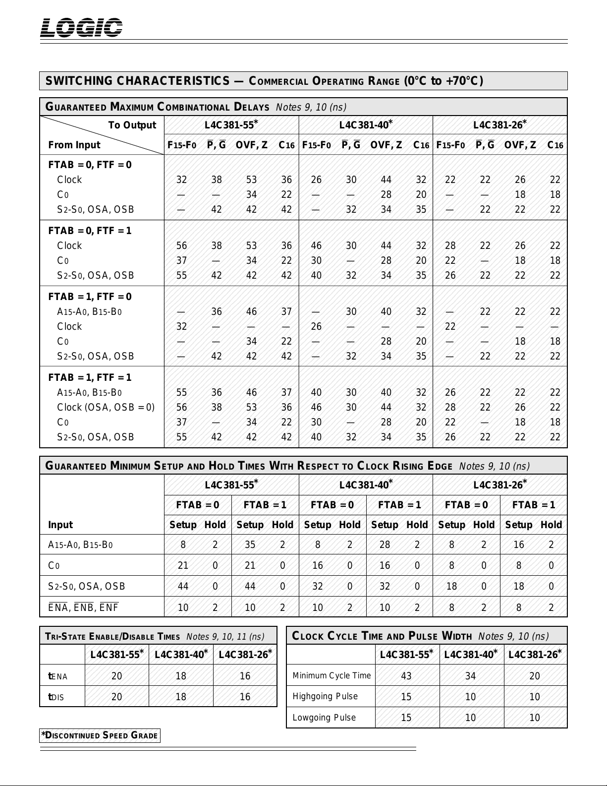
SWITCHING CHARACTERISTICS — COMMERCIAL OPERATING RANGE (0°C to +70°C)
L4C381
GUARANTEED MAXIMUM COMBINATIONAL DELAYS
To Output
From Input
FTAB = 0, FTF = 0
Clock
C0
S2-S0, OSA, OSB
FTAB = 0, FTF = 1
Clock
C0
S2-S0, OSA, OSB
FTAB = 1, FTF = 0
A15-A0, B15-B0
Clock
C0
S2-S0, OSA, OSB
FTAB = 1, FTF = 1
A15-A0, B15-B0
Clock (OSA, OSB = 0)
C0
S2-S0, OSA, OSB
GUARANTEED MINIMUM SETUP AND HOLD TIMES WITH RESPECT TO CLOCK RISING EDGE
Input
A15-A0, B15-B0
C0
S2-S0, OSA, OSB
ENA, ENB, ENF
TRI-STATE ENABLE/DISABLE TIMES
tENA
tDIS
2345678901234567890123
*DISCONTINUED SPEED GRADE
234567890123456789012345678901212345
234567890123456789012345678901212345
234567890123456789012345678901212345
L4C381-55*L4C381-40*L4C381-26
234567890123456789012345678901212345
234567890123456789012345678901212345
234567890123456789012345678901212345
234567890123456789012345678901212345
20 18 16
234567890123456789012345678901212345
234567890123456789012345678901212345
234567890123456789012345678901212345
234567890123456789012345678901212345
20 18 16
2345678901234567890123456789012123456789012345678901234567890121234567890123
2345678901234567890123456789012123456789012345678901234567890121234567890123
2345678901234567890123456789012123456789012345678901234567890121234567890123
2345678901234567890123456789012123456789012345678901234567890121234567890123
2345678901234567890123456789012123456789012345678901234567890121234567890123
2345678901234567890123456789012123456789012345678901234567890121234567890123
2345678901234567890123456789012123456789012345678901234567890121234567890123
F15-F0 P, G OVF, Z C16
2345678901234567890123456789012123456789012345678901234567890121234567890123
2345678901234567890123456789012123456789012345678901234567890121234567890123
2345678901234567890123456789012123456789012345678901234567890121234567890123
2345678901234567890123456789012123456789012345678901234567890121234567890123
2345678901234567890123456789012123456789012345678901234567890121234567890123
2345678901234567890123456789012123456789012345678901234567890121234567890123
2345678901234567890123456789012123456789012345678901234567890121234567890123
2345678901234567890123456789012123456789012345678901234567890121234567890123
2345678901234567890123456789012123456789012345678901234567890121234567890123
2345678901234567890123456789012123456789012345678901234567890121234567890123
2345678901234567890123456789012123456789012345678901234567890121234567890123
2345678901234567890123456789012123456789012345678901234567890121234567890123
2345678901234567890123456789012123456789012345678901234567890121234567890123
2345678901234567890123456789012123456789012345678901234567890121234567890123
2345678901234567890123456789012123456789012345678901234567890121234567890123
2345678901234567890123456789012123456789012345678901234567890121234567890123
2345678901234567890123456789012123456789012345678901234567890121234567890123
2345678901234567890123456789012123456789012345678901234567890121234567890123
2345678901234567890123456789012123456789012345678901234567890121234567890123
2345678901234567890123456789012123456789012345678901234567890121234567890123
2345678901234567890123456789012123456789012345678901234567890121234567890123
2345678901234567890123456789012123456789012345678901234567890121234567890123
2345678901234567890123456789012123456789012345678901234567890121234567890123
2345678901234567890123456789012123456789012345678901234567890121234567890123
2345678901234567890123456789012123456789012345678901234567890121234567890123
2345678901234567890123456789012123456789012345678901234567890121234567890123
2345678901234567890123456789012123456789012345678901234567890121234567890123
2345678901234567890123456789012123456789012345678901234567890121234567890123
2345678901234567890123456789012123456789012345678901234567890121234567890123
2345678901234567890123456789012123456789012345678901234567890121234567890123
2345678901234567890123456789012123456789012345678901234567890121234567890123
2345678901234567890123456789012123456789012345678901234567890121234567890123
2345678901234567890123456789012123456789012345678901234567890121234567890123
2345678901234567890123456789012123456789012345678901234567890121234567890123
2345678901234567890123456789012123456789012345678901234567890121234567890123
2345678901234567890123456789012123456789012345678901234567890121234567890123
2345678901234567890123456789012123456789012345678901234567890121234567890123
2345678901234567890123456789012123456789012345678901234567890121234567890123
2345678901234567890123456789012123456789012345678901234567890121234567890123
2345678901234567890123456789012123456789012345678901234567890121234567890123
2345678901234567890123456789012123456789012345678901234567890121234567890123
2345678901234567890123456789012123456789012345678901234567890121234567890123
2345678901234567890123456789012123456789012345678901234567890121234567890123
2345678901234567890123456789012123456789012345678901234567890121234567890123
2345678901234567890123456789012123456789012345678901234567890121234567890123
2345678901234567890123456789012123456789012345678901234567890121234567890123
2345678901234567890123456789012123456789012345678901234567890121234567890123
2345678901234567890123456789012123456789012345678901234567890121234567890123
2345678901234567890123456789012123456789012345678901234567890121234567890123
2345678901234567890123456789012123456789012345678901234567890121234567890123
2345678901234567890123456789012123456789012345678901234567890121234567890123
2345678901234567890123456789012123456789012345678901234567890121234567890123
2345678901234567890123456789012123456789012345678901234567890121234567890123
2345678901234567890123456789012123456789012345678901234567890121234567890123
2345678901234567890123456789012123456789012345678901234567890121234567890123
2345678901234567890123456789012123456789012345678901234567890121234567890123
2345678901234567890123456789012123456789012345678901234567890121234567890123
2345678901234567890123456789012123456789012345678901234567890121234567890123
2345678901234567890123456789012123456789012345678901234567890121234567890123
2345678901234567890123456789012123456789012345678901234567890121234567890123
2345678901234567890123456789012123456789012345678901234567890121234567890123
2345678901234567890123456789012123456789012345678901234567890121234567890123
2345678901234567890123456789012123456789012345678901234567890121234567890123
2345678901234567890123456789012123456789012345678901234567890121234567890123
2345678901234567890123456789012123456789012345678901234567890121234567890123
2345678901234567890123456789012123456789012345678901234567890121234567890123
Setup Hold Setup Hold
2345678901234567890123456789012123456789012345678901234567890121234567890123
2345678901234567890123456789012123456789012345678901234567890121234567890123
2345678901234567890123456789012123456789012345678901234567890121234567890123
2345678901234567890123456789012123456789012345678901234567890121234567890123
2345678901234567890123456789012123456789012345678901234567890121234567890123
2345678901234567890123456789012123456789012345678901234567890121234567890123
2345678901234567890123456789012123456789012345678901234567890121234567890123
2345678901234567890123456789012123456789012345678901234567890121234567890123
2345678901234567890123456789012123456789012345678901234567890121234567890123
2345678901234567890123456789012123456789012345678901234567890121234567890123
2345678901234567890123456789012123456789012345678901234567890121234567890123
2345678901234567890123456789012123456789012345678901234567890121234567890123
2345678901234567890123456789012123456789012345678901234567890121234567890123
2345678901234567890123456789012123456789012345678901234567890121234567890123
2345678901234567890123456789012123456789012345678901234567890121234567890123
2345678901234567890123456789012123456789012345678901234567890121234567890123
L4C381-55
32 38 53 36
— — 34 22
—424242
56 38 53 36
37 — 34 22
55 42 42 42
—364637
32———
— — 34 22
—424242
55 36 46 37
56 38 53 36
37 — 34 22
55 42 42 42
L4C381-55
FTAB = 0 FTAB = 1
82352
21 0 21 0
44 0 44 0
10 2 10 2
Notes 9, 10, 11 (ns)
Notes 9, 10 (ns)
*
F15-F0 P, G OVF, Z C16
*
Setup Hold Setup Hold
CLOCK CYCLE TIME AND PULSE WIDTH
*
Minimum Cycle Time
Highgoing Pulse
Lowgoing Pulse
4
L4C381-40
*
F15-F0 P, G OVF, Z C16
26 30 44 32
— — 28 20
—323435
46 30 44 32
30 — 28 20
40 32 34 35
—304032
26———
— — 28 20
—323435
40 30 40 32
46 30 44 32
30 — 28 20
40 32 34 35
L4C381-40
FTAB = 0 FTAB = 1
82282
16 0 16 0
32 0 32 0
10 2 10 2
*
234567890123456789012345678901212345
234567890123456789012345678901212345
L4C381-55*L4C381-40*L4C381-26
234567890123456789012345678901212345
234567890123456789012345678901212345
234567890123456789012345678901212345
234567890123456789012345678901212345
43 34 20
234567890123456789012345678901212345
234567890123456789012345678901212345
234567890123456789012345678901212345
234567890123456789012345678901212345
15 10 10
234567890123456789012345678901212345
234567890123456789012345678901212345
234567890123456789012345678901212345
234567890123456789012345678901212345
15 10 10
234567890123456789012345678901212345
Setup Hold Setup Hold
Arithmetic Logic Units
L4C381-26
*
22 22 26 22
— — 18 18
—222222
28 22 26 22
22 — 18 18
26 22 22 22
—222222
22———
— — 18 18
—222222
26 22 22 22
28 22 26 22
22 — 18 18
26 22 22 22
Notes 9, 10 (ns)
L4C381-26
*
FTAB = 0 FTAB = 1
82162
80 80
18 0 18 0
82 82
Notes 9, 10 (ns)
*
08/16/2000–LDS.381-P
Page 5

DEVICES INCORPORATED
16-bit Cascadable ALU
SWITCHING CHARACTERISTICS — COMMERCIAL OPERATING RANGE (0°C to +70°C)
L4C381
GUARANTEED MAXIMUM COMBINATIONAL DELAYS
To Output
From Input
FTAB = 0, FTF = 0
Clock
C0
S2-S0, OSA, OSB
FTAB = 0, FTF = 1
Clock
C0
S2-S0, OSA, OSB
FTAB = 1, FTF = 0
A15-A0, B15-B0
Clock
C0
S2-S0, OSA, OSB
FTAB = 1, FTF = 1
A15-A0, B15-B0
Clock (OSA, OSB = 0)
C0
S2-S0, OSA, OSB
F15-F0 P, G OVF, Z C16
11 20 20 20
— — 14 14
—182018
20 20 20 20
18 — 14 14
20 18 20 18
—162017
11———
— — 14 14
—182018
20 16 20 17
20 20 20 20
18 — 14 14
20 18 20 18
L4C381-20
Notes 9, 10 (ns)
L4C381-15
F15-F0 P, G OVF, Z C16
11 15 15 15
— — 13 13
—141514
15 15 15 15
14 — 13 13
15 14 15 14
—141514
11 — — —
— — 13 13
—141514
15 14 15 14
15 15 15 15
14 — 13 13
15 14 15 14
GUARANTEED MINIMUM SETUP AND HOLD TIMES WITH RESPECT TO CLOCK RISING EDGE
L4C381-15
50120
10 0 10 0
12 0 12 0
50 50
L4C381-20 L4C381-15
18 14
54
54
Input
A15-A0, B15-B0
C0
S2-S0, OSA, OSB
ENA, ENB, ENF
TRI-STATE ENABLE/DISABLE TIMES
L4C381-20 L4C381-15
tENA
tDIS
86
86
Setup Hold Setup Hold
L4C381-20
FTAB = 0 FTAB = 1
50140
12 0 12 0
15 0 15 0
50 50
Notes 9, 10, 11 (ns)
CLOCK CYCLE TIME AND PULSE WIDTH
Minimum Cycle Time
Highgoing Pulse
Lowgoing Pulse
FTAB = 0 FTAB = 1
Setup Hold Setup Hold
Arithmetic Logic Units
5
Notes 9, 10 (ns)
Notes 9, 10 (ns)
08/16/2000–LDS.381-P
Page 6

DEVICES INCORPORATED
4
4
4
4
4
4
4
4
4
4
4
4
4
4
4
4
4
4
4
4
4
4
4
4
4
4
4
4
4
4
4
4
4
4
4
4
4
4
4
4
4
4
4
4
4
4
4
4
4
4
4
4
4
4
4
4
4
4
4
4
4
4
6
6
6
6
6
6
6
6
6
6
6
6
6
6
6
5
5
5
5
5
5
5
5
5
5
5
4
4
4
4
4
4
4
4
4
4
4
4
4
4
4
4
4
4
4
4
4
4
4
4
4
4
4
4
16-bit Cascadable ALU
SWITCHING CHARACTERISTICS — MILITARY OPERATING RANGE (–55°C to +125°C)
L4C381
GUARANTEED MAXIMUM COMBINATIONAL DELAYS
2345678901234567890123456789012123456789012345678901234567890121234567890123
To Output
From Input
FTAB = 0, FTF = 0
Clock
C0
S2-S0, OSA, OSB
FTAB = 0, FTF = 1
Clock
C0
S2-S0, OSA, OSB
FTAB = 1, FTF = 0
A15-A0, B15-B0
Clock
C0
S2-S0, OSA, OSB
FTAB = 1, FTF = 1
A15-A0, B15-B0
Clock (OSA, OSB = 0)
C0
S2-S0, OSA, OSB
GUARANTEED MINIMUM SETUP AND HOLD TIMES WITH RESPECT TO CLOCK RISING EDGE
Input
A15-A0, B15-B0
C0
S2-S0, OSA, OSB
ENA, ENB, ENF
TRI-STATE ENABLE/DISABLE TIMES
tENA
tDIS
2345678901234567890123
2345678901234567890123
*DISCONTINUED SPEED GRADE
23456789012345678901234567890121234
23456789012345678901234567890121234
L4C381-65*L4C381-45*L4C381-30
23456789012345678901234567890121234
23456789012345678901234567890121234
23456789012345678901234567890121234
23456789012345678901234567890121234
22 20 18
23456789012345678901234567890121234
23456789012345678901234567890121234
23456789012345678901234567890121234
23456789012345678901234567890121234
22 20 18
23456789012345678901234567890121234
2345678901234567890123456789012123456789012345678901234567890121234567890123
2345678901234567890123456789012123456789012345678901234567890121234567890123
2345678901234567890123456789012123456789012345678901234567890121234567890123
2345678901234567890123456789012123456789012345678901234567890121234567890123
2345678901234567890123456789012123456789012345678901234567890121234567890123
F15-F0 P, G OVF, Z C16
2345678901234567890123456789012123456789012345678901234567890121234567890123
2345678901234567890123456789012123456789012345678901234567890121234567890123
2345678901234567890123456789012123456789012345678901234567890121234567890123
2345678901234567890123456789012123456789012345678901234567890121234567890123
2345678901234567890123456789012123456789012345678901234567890121234567890123
2345678901234567890123456789012123456789012345678901234567890121234567890123
2345678901234567890123456789012123456789012345678901234567890121234567890123
2345678901234567890123456789012123456789012345678901234567890121234567890123
2345678901234567890123456789012123456789012345678901234567890121234567890123
2345678901234567890123456789012123456789012345678901234567890121234567890123
2345678901234567890123456789012123456789012345678901234567890121234567890123
2345678901234567890123456789012123456789012345678901234567890121234567890123
2345678901234567890123456789012123456789012345678901234567890121234567890123
2345678901234567890123456789012123456789012345678901234567890121234567890123
2345678901234567890123456789012123456789012345678901234567890121234567890123
2345678901234567890123456789012123456789012345678901234567890121234567890123
2345678901234567890123456789012123456789012345678901234567890121234567890123
2345678901234567890123456789012123456789012345678901234567890121234567890123
2345678901234567890123456789012123456789012345678901234567890121234567890123
2345678901234567890123456789012123456789012345678901234567890121234567890123
2345678901234567890123456789012123456789012345678901234567890121234567890123
2345678901234567890123456789012123456789012345678901234567890121234567890123
2345678901234567890123456789012123456789012345678901234567890121234567890123
2345678901234567890123456789012123456789012345678901234567890121234567890123
2345678901234567890123456789012123456789012345678901234567890121234567890123
2345678901234567890123456789012123456789012345678901234567890121234567890123
2345678901234567890123456789012123456789012345678901234567890121234567890123
2345678901234567890123456789012123456789012345678901234567890121234567890123
2345678901234567890123456789012123456789012345678901234567890121234567890123
2345678901234567890123456789012123456789012345678901234567890121234567890123
2345678901234567890123456789012123456789012345678901234567890121234567890123
2345678901234567890123456789012123456789012345678901234567890121234567890123
2345678901234567890123456789012123456789012345678901234567890121234567890123
2345678901234567890123456789012123456789012345678901234567890121234567890123
2345678901234567890123456789012123456789012345678901234567890121234567890123
2345678901234567890123456789012123456789012345678901234567890121234567890123
2345678901234567890123456789012123456789012345678901234567890121234567890123
2345678901234567890123456789012123456789012345678901234567890121234567890123
2345678901234567890123456789012123456789012345678901234567890121234567890123
2345678901234567890123456789012123456789012345678901234567890121234567890123
2345678901234567890123456789012123456789012345678901234567890121234567890123
2345678901234567890123456789012123456789012345678901234567890121234567890123
2345678901234567890123456789012123456789012345678901234567890121234567890123
2345678901234567890123456789012123456789012345678901234567890121234567890123
2345678901234567890123456789012123456789012345678901234567890121234567890123
2345678901234567890123456789012123456789012345678901234567890121234567890123
2345678901234567890123456789012123456789012345678901234567890121234567890123
2345678901234567890123456789012123456789012345678901234567890121234567890123
2345678901234567890123456789012123456789012345678901234567890121234567890123
2345678901234567890123456789012123456789012345678901234567890121234567890123
2345678901234567890123456789012123456789012345678901234567890121234567890123
2345678901234567890123456789012123456789012345678901234567890121234567890123
2345678901234567890123456789012123456789012345678901234567890121234567890123
2345678901234567890123456789012123456789012345678901234567890121234567890123
2345678901234567890123456789012123456789012345678901234567890121234567890123
2345678901234567890123456789012123456789012345678901234567890121234567890123
2345678901234567890123456789012123456789012345678901234567890121234567890123
2345678901234567890123456789012123456789012345678901234567890121234567890123
2345678901234567890123456789012123456789012345678901234567890121234567890123
2345678901234567890123456789012123456789012345678901234567890121234567890123
2345678901234567890123456789012123456789012345678901234567890121234567890123
2345678901234567890123456789012123456789012345678901234567890121234567890123
2345678901234567890123456789012123456789012345678901234567890121234567890123
2345678901234567890123456789012123456789012345678901234567890121234567890123
2345678901234567890123456789012123456789012345678901234567890121234567890123
2345678901234567890123456789012123456789012345678901234567890121234567890123
2345678901234567890123456789012123456789012345678901234567890121234567890123
Setup Hold Setup Hold
2345678901234567890123456789012123456789012345678901234567890121234567890123
2345678901234567890123456789012123456789012345678901234567890121234567890123
2345678901234567890123456789012123456789012345678901234567890121234567890123
2345678901234567890123456789012123456789012345678901234567890121234567890123
2345678901234567890123456789012123456789012345678901234567890121234567890123
2345678901234567890123456789012123456789012345678901234567890121234567890123
2345678901234567890123456789012123456789012345678901234567890121234567890123
2345678901234567890123456789012123456789012345678901234567890121234567890123
2345678901234567890123456789012123456789012345678901234567890121234567890123
2345678901234567890123456789012123456789012345678901234567890121234567890123
2345678901234567890123456789012123456789012345678901234567890121234567890123
2345678901234567890123456789012123456789012345678901234567890121234567890123
2345678901234567890123456789012123456789012345678901234567890121234567890123
2345678901234567890123456789012123456789012345678901234567890121234567890123
2345678901234567890123456789012123456789012345678901234567890121234567890123
L4C381-65
37 44 63 45
— — 42 25
—484848
68 44 63 45
42 — 42 25
66 48 48 48
—445644
37———
— — 42 25
—484848
65 44 56 44
68 44 63 45
42 — 42 25
66 48 48 48
L4C381-65
FTAB = 0 FTAB = 1
10 3 43 3
25 0 25 0
50 0 50 0
12 2 12 2
Notes 9, 10, 11 (ns)
Notes 9, 10 (ns)
*
F15-F0 P, G OVF, Z C16
*
Setup Hold Setup Hold
CLOCK CYCLE TIME AND PULSE WIDTH
*
Minimum Cycle Time
Highgoing Pulse
Lowgoing Pulse
6
L4C381-45
*
F15-F0 P, G OVF, Z C16
28 34 50 34
— — 32 23
—383838
56 34 50 34
32 — 32 23
46 38 38 38
—324636
28 — — —
— — 32 23
—383838
45 32 46 36
56 34 50 34
32 — 32 23
46 38 38 38
*
L4C381-45
FTAB = 0 FTAB = 1
83333
20 0 20 0
36 0 36 0
10 2 10 2
234567890123456789012345678901212345
234567890123456789012345678901212345
L4C381-65*L4C381-45*L4C381-30
234567890123456789012345678901212345
234567890123456789012345678901212345
234567890123456789012345678901212345
234567890123456789012345678901212345
52 38 26
234567890123456789012345678901212345
234567890123456789012345678901212345
234567890123456789012345678901212345
234567890123456789012345678901212345
20 15 12
234567890123456789012345678901212345
234567890123456789012345678901212345
234567890123456789012345678901212345
234567890123456789012345678901212345
20 15 12
234567890123456789012345678901212345
Setup Hold Setup Hold
Arithmetic Logic Units
L4C381-30
*
26 28 34 28
— — 22 22
—282828
34 28 34 28
26 — 22 22
30 28 28 28
—282828
26———
— — 22 22
—282828
30 28 28 28
34 28 34 28
26 — 22 22
30 28 28 28
Notes 9, 10 (ns)
L4C381-30
*
FTAB = 0 FTAB = 1
83203
12 0 12 0
20 0 20 0
10 2 10 2
Notes 9, 10 (ns)
*
08/16/2000–LDS.381-P
Page 7

DEVICES INCORPORATED
6
6
6
6
6
6
6
6
6
6
6
6
6
6
6
5
5
5
5
5
5
5
5
5
5
5
0
0
0
0
0
0
0
0
0
0
0
0
0
0
0
0
0
0
0
0
0
0
0
0
0
0
0
0
0
0
0
0
0
0
0
0
0
0
0
0
0
0
0
0
0
0
0
0
0
0
0
0
0
0
0
0
0
0
0
0
0
0
0
0
0
0
0
0
0
0
0
0
0
0
0
0
0
0
0
0
0
0
0
0
0
0
0
0
0
4
4
16-bit Cascadable ALU
SWITCHING CHARACTERISTICS — MILITARY OPERATING RANGE (–55°C to +125°C)
L4C381
GUARANTEED MAXIMUM COMBINATIONAL DELAYS
23456789012345678901234567890121234567890123456789
To Output
From Input
FTAB = 0, FTF = 0
Clock
C0
S2-S0, OSA, OSB
FTAB = 0, FTF = 1
Clock
C0
S2-S0, OSA, OSB
FTAB = 1, FTF = 0
A15-A0, B15-B0
Clock
C0
S2-S0, OSA, OSB
FTAB = 1, FTF = 1
A15-A0, B15-B0
Clock (OSA, OSB = 0)
C0
S2-S0, OSA, OSB
GUARANTEED MINIMUM SETUP AND HOLD TIMES WITH RESPECT TO CLOCK RISING EDGE
Input
A15-A0, B15-B0
C0
S2-S0, OSA, OSB
ENA, ENB, ENF
TRI-STATE ENABLE/DISABLE TIMES
tENA
tDIS
2345678901234567890123
2345678901234567890123
*DISCONTINUED SPEED GRADE
23456789012345678901234
23456789012345678901234
L4C381-25*L4C381-20
23456789012345678901234
23456789012345678901234
23456789012345678901234
23456789012345678901234
14 10
23456789012345678901234
23456789012345678901234
23456789012345678901234
23456789012345678901234
14 10
23456789012345678901234
23456789012345678901234567890121234567890123456789
23456789012345678901234567890121234567890123456789
23456789012345678901234567890121234567890123456789
23456789012345678901234567890121234567890123456789
23456789012345678901234567890121234567890123456789
F15-F0 P, G OVF, Z C16
23456789012345678901234567890121234567890123456789
23456789012345678901234567890121234567890123456789
23456789012345678901234567890121234567890123456789
23456789012345678901234567890121234567890123456789
23456789012345678901234567890121234567890123456789
23456789012345678901234567890121234567890123456789
23456789012345678901234567890121234567890123456789
23456789012345678901234567890121234567890123456789
23456789012345678901234567890121234567890123456789
23456789012345678901234567890121234567890123456789
23456789012345678901234567890121234567890123456789
23456789012345678901234567890121234567890123456789
23456789012345678901234567890121234567890123456789
23456789012345678901234567890121234567890123456789
23456789012345678901234567890121234567890123456789
23456789012345678901234567890121234567890123456789
23456789012345678901234567890121234567890123456789
23456789012345678901234567890121234567890123456789
23456789012345678901234567890121234567890123456789
23456789012345678901234567890121234567890123456789
23456789012345678901234567890121234567890123456789
23456789012345678901234567890121234567890123456789
23456789012345678901234567890121234567890123456789
23456789012345678901234567890121234567890123456789
23456789012345678901234567890121234567890123456789
23456789012345678901234567890121234567890123456789
23456789012345678901234567890121234567890123456789
23456789012345678901234567890121234567890123456789
23456789012345678901234567890121234567890123456789
23456789012345678901234567890121234567890123456789
23456789012345678901234567890121234567890123456789
23456789012345678901234567890121234567890123456789
23456789012345678901234567890121234567890123456789
23456789012345678901234567890121234567890123456789
23456789012345678901234567890121234567890123456789
23456789012345678901234567890121234567890123456789
23456789012345678901234567890121234567890123456789
23456789012345678901234567890121234567890123456789
23456789012345678901234567890121234567890123456789
23456789012345678901234567890121234567890123456789
23456789012345678901234567890121234567890123456789
23456789012345678901234567890121234567890123456789
23456789012345678901234567890121234567890123456789
23456789012345678901234567890121234567890123456789
23456789012345678901234567890121234567890123456789
23456789012345678901234567890121234567890123456789
23456789012345678901234567890121234567890123456789
23456789012345678901234567890121234567890123456789
23456789012345678901234567890121234567890123456789
23456789012345678901234567890121234567890123456789
23456789012345678901234567890121234567890123456789
23456789012345678901234567890121234567890123456789
23456789012345678901234567890121234567890123456789
23456789012345678901234567890121234567890123456789
23456789012345678901234567890121234567890123456789
23456789012345678901234567890121234567890123456789
23456789012345678901234567890121234567890123456789
23456789012345678901234567890121234567890123456789
23456789012345678901234567890121234567890123456789
23456789012345678901234567890121234567890123456789
23456789012345678901234567890121234567890123456789
23456789012345678901234567890121234567890123456789
23456789012345678901234567890121234567890123456789
23456789012345678901234567890121234567890123456789
23456789012345678901234567890121234567890123456789
23456789012345678901234567890121234567890123456789
23456789012345678901234567890121234567890123456789
Setup Hold Setup Hold
23456789012345678901234567890121234567890123456789
23456789012345678901234567890121234567890123456789
23456789012345678901234567890121234567890123456789
23456789012345678901234567890121234567890123456789
23456789012345678901234567890121234567890123456789
23456789012345678901234567890121234567890123456789
23456789012345678901234567890121234567890123456789
23456789012345678901234567890121234567890123456789
23456789012345678901234567890121234567890123456789
23456789012345678901234567890121234567890123456789
23456789012345678901234567890121234567890123456789
23456789012345678901234567890121234567890123456789
23456789012345678901234567890121234567890123456789
23456789012345678901234567890121234567890123456789
23456789012345678901234567890121234567890123456789
23456789012345678901234567890121234567890123456789
L4C381-25
14 24 24 24
— — 18 18
—222422
25 24 24 24
21 — 18 18
25 22 24 22
—202522
14———
— — 18 18
—222422
25 20 25 22
25 24 24 24
21 — 18 18
25 22 24 22
L4C381-25
FTAB = 0 FTAB = 1
72142
14 0 14 0
19 0 19 0
70 70
Notes 9, 10, 11 (ns)
*
Notes 9, 10 (ns)
*
F15-F0 P, G OVF, Z C16
*
Setup Hold Setup Hold
CLOCK CYCLE TIME AND PULSE WIDTH
Minimum Cycle Time
Highgoing Pulse
Lowgoing Pulse
7
L4C381-20
*
14 20 20 20
— — 16 16
—182018
20 20 20 20
17 — 16 16
20 18 20 18
—172017
14 — — —
— — 16 16
—182018
20 17 20 17
20 20 20 20
17 — 16 16
20 18 20 18
L4C381-20
*
FTAB = 0 FTAB = 1
62122
12 0 12 0
16 0 16 0
60 60
234567890123456789012345
234567890123456789012345
L4C381-25*L4C381-20
234567890123456789012345
234567890123456789012345
234567890123456789012345
234567890123456789012345
20 18
234567890123456789012345
234567890123456789012345
234567890123456789012345
234567890123456789012345
86
234567890123456789012345
234567890123456789012345
234567890123456789012345
234567890123456789012345
86
234567890123456789012345
Arithmetic Logic Units
Notes 9, 10 (ns)
Notes 9, 10 (ns)
*
08/16/2000–LDS.381-P
Page 8

DEVICES INCORPORATED
OE
0.2 V
t
DIS
t
ENA
0.2 V
1.5 V 1.5 V
3.5V Vth
1
Z
0
Z
Z
1
Z
0
1.5 V
1.5 V
0V Vth
VOL*
V
OH
*
V
OL
*
V
OH
*
Measured V
OL
with IOH = –10mA and IOL = 10mA
Measured V
OH
with IOH = –10mA and IOL = 10mA
NOTES
L4C381
16-bit Cascadable ALU
1. Maximum Ratings indicate stress
specifications only. Functional operation of these products at values beyond
those indicated in the Operating Conditions table is not implied. Exposure to
maximum rating conditions for extended periods may affect reliability.
2. The products described by this specification include internal circuitry designed to protect the chip from damaging substrate injection currents and accumulations of static charge. Nevertheless, conventional precautions should
be observed during storage, handling,
and use of these circuits in order to
avoid exposure to excessive electrical
stress values.
3. This device provides hard clamping of
transient undershoot and overshoot. Input levels below ground or above VCC
will be clamped beginning at –0.6 V and
VCC + 0.6 V. The device can withstand
indefinite operation with inputs in the
range of –0.5 V to +7.0 V. Device operation will not be adversely affected, however, input current levels will be well in
excess of 100 mA.
9. AC specifications are tested with
input transition times less than 3 ns,
output reference levels of 1.5 V (except
tDIS test), and input levels of nominally
0 to 3.0 V. Output loading may be a
resistive divider which provides for
specified IOH and IOL at an output
voltage of VOH min and VOL max
respectively. Alternatively, a diode
bridge with upper and lower current
sources of IOH and IOL respectively,
and a balancing voltage of 1.5 V may be
used. Parasitic capacitance is 30 pF
minimum, and may be distributed.
This device has high-speed outputs capable of large instantaneous current
pulses and fast turn-on/turn-off times.
As a result, care must be exercised in the
testing of this device. The following
measures are recommended:
a. A 0.1 µF ceramic capacitor should be
installed between VCC and Ground
leads as close to the Device Under Test
(DUT) as possible. Similar capacitors
should be installed between device VCC
and the tester common, and device
ground and tester common.
11. For the tENA test, the transition is
measured to the 1.5 V crossing point
with datasheet loads. For the tDIS test,
the transition is measured to the
±200mV level from the measured
steady-state output voltage with
±10mA loads. The balancing voltage, VTH, is set at 3.5 V for Z-to-0
and 0-to-Z tests, and set at 0 V for Zto-1 and 1-to-Z tests.
12. These parameters are only tested at
the high temperature extreme, which is
the worst case for leakage current.
FIGURE A. OUTPUT LOADING CIRCUIT
DUT
S1
I
OL
V
C
L
I
TH
OH
FIGURE B. THRESHOLD LEVELS
4. Actual test conditions may vary from
those designated but operation is guaranteed as specified.
5. Supply current for a given application can be accurately approximated by:
2
NCV F
where
4
N = total number of device outputs
C = capacitive load per output
V = supply voltage
F = clock frequency
b. Ground and VCC supply planes
must be brought directly to the DUT
socket or contactor fingers.
c. Input voltages should be adjusted to
compensate for inductive ground and VCC
noise to maintain required DUT input
levels relative to the DUT ground pin.
10. Each parameter is shown as a minimum or maximum value. Input requirements are specified from the point
of view of the external system driving
the chip. Setup time, for example, is
specified as a minimum since the exter-
6. Tested with all outputs changing every cycle and no load, at a 5 MHz clock
rate.
nal system must supply at least that
much time to meet the worst-case requirements of all parts. Responses from
the internal circuitry are specified from
7. Tested with all inputs within 0.1 V of
VCC or Ground, no load.
8. These parameters are guaranteed
but not 100% tested.
the point of view of the device. Output
delay, for example, is specified as a
maximum since worst-case operation of
any device always provides data within
that time.
8
Arithmetic Logic Units
08/16/2000–LDS.381-P
Page 9

DEVICES INCORPORATED
CASCADING THE L4C381
L4C381
16-bit Cascadable ALU
Cascading the L4C381 to 32 bits is
accomplished simply by connecting
the C16 output of the least significant
slice to the C0 input of the most significant slice. The S2-S0, OSA, OSB,
ENA, ENB, and ENF lines are
common to both devices. The Zero
output flags should be logically
ANDed to produce the Zero flag for
the 32-bit result. The OVF and C16
outputs of the most significant slice
are valid for the 32-bit result.
Propagation delay calculations for this
configuration require two steps: First
determine the propagation delay from
the input of interest to the C16 output
of the lower slice. Add this number
to the delay from the C0 input of the
upper slice to the output of interest
(of the C0 setup time, if the F register
is used). The sum gives the overall
input-to-output delay (or setup time)
for the 32-bit configuration. This
method gives a conservative result,
since the C16 output is very lightly
loaded. Formulas for calculation of
all critical delays for a 32-bit system
are shown in Figures 4A through 4D.
Cascading to greater than 32 bits can
be accomplished in two ways: The
simplest (but slowest) method is to
simply connect the C16 output of each
slice to the C0 input of the next more
significant slice. Propagation delays
are calculated as for the 32-bit case,
except that the C0 to C16 delays for all
intermediate slices must be added to
the overall delay for each path. A
faster method is to use an external
carry-lookahead generator. The P and
G outputs of each slice are connected
as inputs to the CLA generator, which
in turn produces the C0 inputs for
each slice except the least significant.
The C16 outputs are not used in this
case, except for the most significant
one, which is the carry out of the
overall system. The carry in to the
system is connected to the C0 input of
the least significant slice, and also to
the carry lookahead generator.
Propagation delays for this configuration are the sum of the time to P, G,
for the least significant slice, the
propagation delay of the carry lookahead generator, and the C0 to output
time of the most significant slice.
Arithmetic Logic Units
9
08/16/2000–LDS.381-P
Page 10

DEVICES INCORPORATED
FIGURE 4A. FTAB = 0, FTF = 0
From To Calculated Specification Limit
Clock ➞ F = Same as 16-bit case
Clock ➞ Other = (Clock ➞ C16) + (C0 ➞ Out)
C0 ➞ Other = (C0 ➞ C16) + (C0 ➞ Out)
S2-S0, OSA, OSB ➞ Other = (S2-S0, OSA, OSB ➞ C16) + (C0 ➞ Out)
A, B Setup time = Same as 16-bit case
C0 Setup time = (C0 ➞ C16) + (C0 Setup time)
S2-S0, OSA, OSB Setup time = (S2-S0, OSA, OSB ➞ C16) + (C0 Setup time)
ENA, ENB, ENF Setup time = Same as 16-bit case
Minimum cycle time = (Clock ➞ C16) + (C0 Setup time)
A31-A
L4C381
16-bit Cascadable ALU
16
B31-B
16
A15-A
0
B15-B
0
D
Q
A
MOST
16
SIGNIFICANT
SLICE
FIGURE 4B. FTAB = 0, FTF = 1
From To Calculated Specification Limit
Clock ➞ F = (Clock ➞ C16) + (C0 ➞ F)
Clock ➞ Other = (Clock ➞ C16) + (C0 ➞ Out)
C0 ➞ F = (C0 ➞ C16) + (C0 ➞ F)
C0 ➞ Other = (C0 ➞ C16) + (C0 ➞ Out)
S2-S0, OSA, OSB ➞ F = (S2-S0, OSA, OSB ➞ C16) + (C0 ➞ F)
S2-S0, OSA, OSB ➞ Other = (S2-S0, OSA, OSB ➞ C16) + (C0 ➞ Out)
A, B Setup time = Same as 16-bit case
C0 Setup time = (C0 ➞ C16) + (C0 Setup time)
S2-S0, OSA, OSB Setup time = (S2-S0, OSA, OSB ➞ C16) + (C0 Setup time)
ENA, ENB, ENF Setup time = Same as 16-bit case
Minimum cycle time = (Clock ➞ C16) + (C0 Setup time)
F
D
F31-F
D
Q
B
0
C
Q
CLOCK CLOCK
D
Q
A
16
C
16
D
Q
B
C
F
D
Q
0
CLOCK
S
C
0,
OSA, OSB
2–S0
LEAST
SIGNIFICANT
F15-F
16
0
SLICE
MOST
SIGNIFICANT
SLICE
A31-A16
D
Q
A
F
16
F31-F16
B31-B16
D
Q
B
0
C
A15-A0 B15-B0
D
Q
A
16
C
10
F
16
F15-F0
D
Q
B
C
0
CLOCK
S
C
0,
OSA, OSB
2–S0
LEAST
SIGNIFICANT
SLICE
Arithmetic Logic Units
08/16/2000–LDS.381-P
Page 11

DEVICES INCORPORATED
FIGURE 4C. FTAB = 1, FTF = 0
From To Calculated Specification Limit
Clock ➞ F = Same as 16-bit case
A, B ➞ Other = (A, B ➞ C16) + (C0 ➞ Out)
C0 ➞ Other = (C0 ➞ C16) + (C0 ➞ Out)
S2-S0, OSA, OSB ➞ Other = (S2-S0, OSA, OSB ➞ C16) + (C0 ➞ Out)
A, B Setup time = (A, B ➞ C16) + (C0 Setup time)
C0 Setup time = (C0 ➞ C16) + (C0 Setup time)
S2-S0, OSA, OSB Setup time = (S2-S0, OSA, OSB ➞ C16) + (C0 Setup time)
ENA, ENB, ENF Setup time = Same as 16-bit case
Minimum cycle time = (Clock ➞ C16) + (C0 Setup time)
(F register accumulate loop)
A31-A
A
L4C381
16-bit Cascadable ALU
16
B31-B
16
B
0
C
F
A15-A
A
16
C
0
B15-B
0
2–S0
S
C
0,
B
C
F
OSA, OSB
0
MOST
16
SIGNIFICANT
SLICE
FIGURE 4D. FTAB = 1, FTF = 1
From To Calculated Specification Limit
A, B ➞ F = (A, B ➞ C16) + (C0 ➞ F)
A, B ➞ Other = (A, B ➞ C16) + (C0 ➞ Out)
C0 ➞ F = (C 0 ➞ C16) + (C0 ➞ F)
C0 ➞ Other = (C0 ➞ C16) + (C0 ➞ Out)
S2-S0, OSA, OSB ➞ F = (S2-S0, OSA, OSB ➞ C16) + (C0 ➞ F)
S2-S0, OSA, OSB ➞ Other = (S2-S0, OSA, OSB ➞ C16) + (C0 ➞ Out)
A, B Setup time = (A, B ➞ C16) + (C0 Setup time)
C0 Setup time = (C0 ➞ C16) + (C0 Setup time)
S2-S0, OSA, OSB Setup time = (S2-S0, OSA, OSB ➞ C16) + (C0 Setup time)
ENA, ENB, ENF Setup time = Same as 16-bit case
Minimum cycle time = (Clock ➞ C16) + (C0 Setup time)
(F register accumulate loop)
D
F31-F
16
D
Q
LEAST
Q
CLOCK CLOCK
SIGNIFICANT
F15-F
16
0
SLICE
MOST
SIGNIFICANT
SLICE
A31-A
A
16
16
F31-F
B31-B
16
B
0
C
F
A15-A
A
16
C
0
16
B15-B
0
2–S0
S
C
0,
B
0
C
F
OSA, OSB
LEAST
SIGNIFICANT
F15-F
16
0
SLICE
Arithmetic Logic Units
11
08/16/2000–LDS.381-P
Page 12

DEVICES INCORPORATED
7
7
7
7
7
7
7
7
7
7
7
7
7
7
7
7
7
7
7
7
7
7
7
7
7
7
7
7
7
7
7
7
7
7
7
7
7
7
7
7
7
7
7
7
7
7
7
7
7
7
7
7
7
7
7
7
7
7
7
7
7
7
7
7
7
7
7
7
7
7
7
A
B
C
D
E
F
G
H
J
K
L
Top View
Through Package
(i.e., Component Side Pinout)
1234567 8 9 10 11
A
8
A
9
A
11
A
13
A
15
V
CC
C
16
G
OVF
OE
F
15
A
7
A
6
F
14
F
13
A
5
A
4
F
12
F
11
A
3
A
2
F
10
F
9
A
1
A
0
F
8
F
7
B
15
B
14
F
6
F
5
B
13
B
12
F
4
F
3
B
11
B
10
F
2
F
1
B
9
B
8
B
5
B
3
B
1
ENA
FTAB
OSA
S
1
C
0
F
0
A
10
A
12
A
14
CLK
GND
P
ZERO
ENF
FTF
B
7
B
6
B
4
B
2
B
0
ENB
OSB
S
2
S
0
ORDERING INFORMATION
68-pin
A8A7A6A5A4A3A2A1A0
46663 6212
10
A9
11
A10
12
A11
13
A12
14
A13
15
A14
16
A15
17
CLK
18
CC
V
19
GND
20
16
C
21
P
22
G
23
ZERO
24
OVF
25
ENF
26
FTF
27 32 33 34 35 36 37 386139 40941 42 43
28 29 30 31
OE
Plastic J-Lead Chip Carrier
Speed
(J2)
0°C to +70°C — COMMERCIAL SCREENING
20 ns
15 ns
–55°C to +125°C — COMMERCIAL SCREENING
–55°C to +125°C — MIL-STD-883 COMPLIANT
L4C381JC20
L4C381JC15
5867
15
F
F14
F13
F12
B15
B14
3
6768 6465
Top
View
F9F8F7F6F5F4F3F2F1
F11
F10
L4C381
16-bit Cascadable ALU
23456789012345678901234567890121234567890123456
23456789012345678901234567890121234567890123456
23456789012345678901234567890121234567890123456
23456789012345678901234567890121234567890123456
23456789012345678901234567890121234567890123456
23456789012345678901234567890121234567890123456
23456789012345678901234567890121234567890123456
68-pin
23456789012345678901234567890121234567890123456
23456789012345678901234567890121234567890123456
23456789012345678901234567890121234567890123456
23456789012345678901234567890121234567890123456
23456789012345678901234567890121234567890123456
B13
B12
B11
B10B9B8
60
B7
59
B6
58
B5
57
B4
56
B3
55
B2
54
B1
53
B0
52
ENA
51
ENB
50
FTAB
49
OSB
48
OSA
47
S
46
S1
45
S0
44
C0
F0
23456789012345678901234567890121234567890123456
23456789012345678901234567890121234567890123456
23456789012345678901234567890121234567890123456
23456789012345678901234567890121234567890123456
23456789012345678901234567890121234567890123456
23456789012345678901234567890121234567890123456
23456789012345678901234567890121234567890123456
23456789012345678901234567890121234567890123456
23456789012345678901234567890121234567890123456
23456789012345678901234567890121234567890123456
23456789012345678901234567890121234567890123456
23456789012345678901234567890121234567890123456
23456789012345678901234567890121234567890123456
23456789012345678901234567890121234567890123456
23456789012345678901234567890121234567890123456
23456789012345678901234567890121234567890123456
23456789012345678901234567890121234567890123456
23456789012345678901234567890121234567890123456
23456789012345678901234567890121234567890123456
23456789012345678901234567890121234567890123456
23456789012345678901234567890121234567890123456
23456789012345678901234567890121234567890123456
23456789012345678901234567890121234567890123456
23456789012345678901234567890121234567890123456
23456789012345678901234567890121234567890123456
23456789012345678901234567890121234567890123456
23456789012345678901234567890121234567890123456
23456789012345678901234567890121234567890123456
23456789012345678901234567890121234567890123456
2
23456789012345678901234567890121234567890123456
23456789012345678901234567890121234567890123456
23456789012345678901234567890121234567890123456
23456789012345678901234567890121234567890123456
23456789012345678901234567890121234567890123456
23456789012345678901234567890121234567890123456
23456789012345678901234567890121234567890123456
23456789012345678901234567890121234567890123456
23456789012345678901234567890121234567890123456
23456789012345678901234567890121234567890123456
23456789012345678901234567890121234567890123456
23456789012345678901234567890121234567890123456
23456789012345678901234567890121234567890123456
23456789012345678901234567890121234567890123456
23456789012345678901234567890121234567890123456
23456789012345678901234567890121234567890123456
23456789012345678901234567890121234567890123456
23456789012345678901234567890121234567890123456
23456789012345678901234567890121234567890123456
23456789012345678901234567890121234567890123456
23456789012345678901234567890121234567890123456
23456789012345678901234567890121234567890123456
23456789012345678901234567890121234567890123456
23456789012345678901234567890121234567890123456
23456789012345678901234567890121234567890123456
23456789012345678901234567890121234567890123456
23456789012345678901234567890121234567890123456
23456789012345678901234567890121234567890123456
23456789012345678901234567890121234567890123456
23456789012345678901234567890121234567890123456
Discontinued Package
Ceramic Pin Grid Array
(G1)
Arithmetic Logic Units
12
08/16/2000–LDS.381-P
 Loading...