

Page 1
L4969
SYSTEM VOLTAGE REGULATOR
WITH FAULT TOLERANT LOW SPEED CAN-TRANSCEIVER
PRELIMINARY DATA
■ OPERATING SU PPLY VOLTAGE 6V TO 28V,
TRANSIENT UP TO 40V
■ LOW QUIESCENT CURRENT CONSUMP-
TION, LESS THA N 40
■ TWO VERY LOW DROP VOLTAGE
REGULATORS 5V / 200mA
AND 5V/200mA
■ SEPARATE VOLTAGE REGULATOR FOR
CAN-TRANSCEIVER SUPPLY WITH LOW
POWER SLEEP MODE
■ EFFICIENT UC SUPERVISION AND RESET
LOGIC
■ 24 BIT SERIAL INTERF AC E
■ AN UNPOWERED OR INSUFFI C IENTLY
SUPPLIED NODE DOES NOT DIST U RB THE
BUS LINES
■ VS VOLTAGE SENSE COMPARATOR
■ SUPPORTS TRANSMISSION WITH
GROUNDSHIFT:
SINGLE WIRE: 1.5V, DIFFERENTIAL: 3V
µA IN SLEEP MODE
SO20 PowerSO20
ORDERING NUMBERS: L4969MD (SO20)
L4969 (PowerSO20)
DESCRIPTION
The L4969 is an integrated circuit containing 3 independent Voltage Regulators and a standard fault tolerant low speed CAN line interface in multipower
BCD3S process.
It integrat es all mai n l ocal functions for automot iv e body
electronic applications conn ected to a CAN bus.
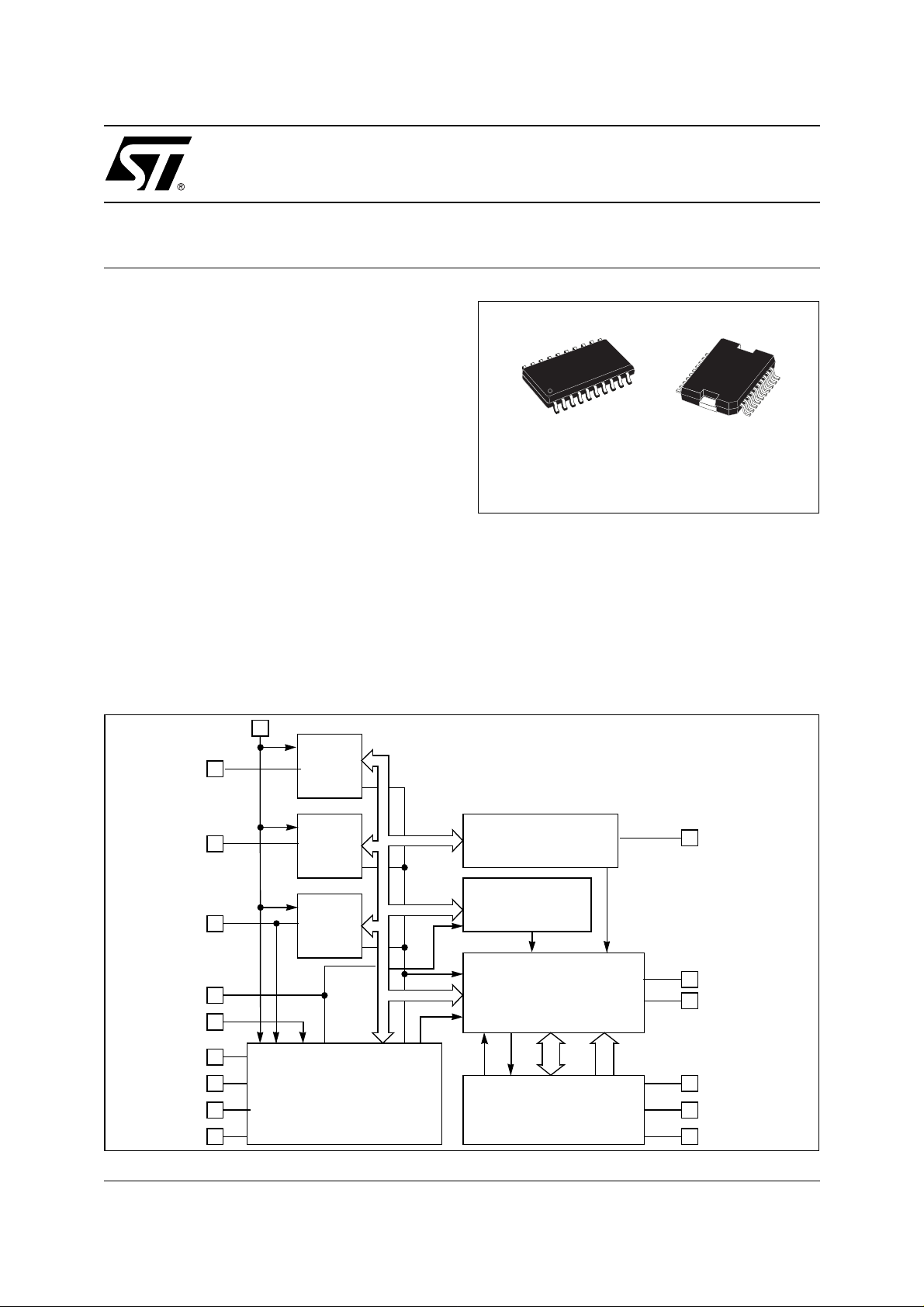
Figure 1. Block Diagram
VS
V1
V2
V3
RX
TX
CANH
RTH
CANL
RTL
VREG 1
VREG 2
VREG 3
Fault tole ran t
low speed
CAN-transceiver
Watchdo g and
adjustable RC-O s cillator
Iden tifier Filter
Control and Status Memory
24 Bit SPI
NRESET
WAKE
NINT
SCLK
SIN
SOUT
August 2003
This is preliminary information on a new product now in development or undergoing evaluation. Details are subject to change without notice.
1/35
Page 2
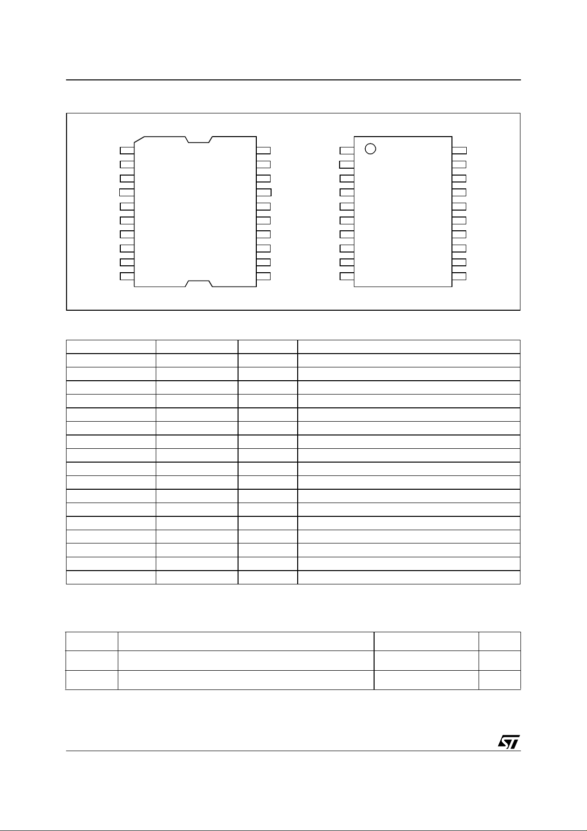
L4969
Figure 2. Pin Connection
GND
V1
V2
V3
VS
CANH
RTL
CANL
RTH
GND
Table 1.
Pin Functions
Pin No. (PSO20) Pin No. (SO20) Pin Name Function
1, 10, 11, 20 5,6, 15, 16 GND Power Ground
2 7 V1 Microcontroller Supply Voltage
3 8 V2 Peripheral Supply Voltage
4 9 V3 Internal CAN Supply
5 10 VS Power Supply
6 11 CANH CANH Line Driver Output
7 12 RTL CANL Termination Source
8 13 CANL CANL Line Driver Output
9 14 RTH CANH Termination Source
12 17 RXD Act. Low CAN Receive Dominant Data Output
13 18 TXD Act. Low CAN Transmit Dominant Data Input
14 19 SOUT Serial Data Output
15 20 SIN Serial Data Input
16 1 SCLK Serial Clock
17 2 NRES Act. Low Reset Output
18 3 NINT Act. Low Interrupt Request
19 4 WAKE Dual Edge Triggerable Wakeup Input
PSO20
GND
WAKE
NINT
NRES
SCLK
SIN
SOUT
TXD
RXD
GND
SCLK
NRES
NINT
WAKE
GND
GND
V1
V2
V3
VS
SO20
SIN
SOUT
TX
RX
GND
GND
RTH
CANL
RTL
CANH
Table 2. Thermal Data
Symbol Parameter Value Unit
R
thj-amb
R
thj-case
Note: 1. Typical value soldered on a PC board wit h 8 cm2 copper ground plane (35µm thick).
2/35
Thermal resistance junction-ambient
Thermal resistance junction-case 3 °C/W
40
1)
°C/W
Page 3

Table 3. Absolute Maximum Ratings
Symbol Parameter Value Unit
V
VSDC
V
VSTR
I
VOUT1...3
T
STG
T
V
OUT1
V
OUT2
V
OUT3
V
inli
V
inliW
V
canh
V
canl
Notes: 1. All pins of the IC are protect ed against ESD. The verifi cation is perf ormed according to MIL 883C,
2. Voltage forced means voltage limited to the specified values whil e the current is not limited.
3. ESD Pulses on CAN-Pins up to 4K V HBM vs GND with all other P i ns grounded.
DC operating supply voltage -0.3 ... +28 V
Transient operating supply voltage (T < 400ms) -0.3 ... +40 V
Output currents Internally limited
Storage temperature -65 ... +150 T
Operating junction temperature -40 ... +150 T
J
Externally forced output voltage OUT1 -0.3 ... VS+0.3, max +6.3 V
Externally forced output voltage OUT2 -0.3 ... VS+0.3 V
Externally forced output voltage OUT3 -0.3 ... VS+0.3, max +6.3 V
Input voltage Logic inputs: SIN, SCLK, NRES -0.3 ... +7 V
Input voltage WAKE -0.3 ... VS+0.3 V
Voltage CANH line
Voltage CANL line
human body model with R = 1.5kW, C = 100pF and dischar ge voltage 200 0V,
corresponding to a maximum disch arge energy of 0.2mJ..
3
3
-28 ... +40 V
-28 ... +40 V
L4969
VSDC
VSTR
I
VOUT1...3
STG
J
OUT1
OUT2
OUT3
inli
inliW
canh
canl
Table 4. Electrical Characteristics
V
= 14V, Tj=-40°C to 150°C unless otherwise specified.
S
Symbol Parameter Test Conditions Min. Typ. Max. Unit
Supply Current
I
SSL
All Regulators off
(CANH Standby
I
SSLWK
V1 off, V2 off, V3 on
(CAN RX only)
I
SSB
I
S
V1 only (CAN Standby) Timer off (Standby #1) 150 250 µA
All Regulators on,
(CAN active, TX high)
I
SCP
Additional Oscillator- and
Chargepumpcurrent at low VS
Voltage Regulator 1
V
01
V
DP1
V1 output voltage 6V < VS < 28V
Dropout voltage 1@ VS=4.8V I
Timer off (Sleep #1) 30 40 60 µA
Timer on (Sleep #2) 70 90 135 µA
RXonly 4 6 mA
Timer on (Standby #2) 200 300 µA
Default (Standby #3) 440 600 µA
I
OUT1
I
OUT2
= -100mA
= -10mA
120 150 mA
No CAN load.
VS = 6V; Timer Off 55 80 100 µA
= 6V; Timer On 10 30 50 µA
V
S
4.9 5 5.1 V
IO >-100mA
SO20 Package
6V < V
I
>-150mA
O
< 28V
S
4.9 5 5.1 V
PSO20 Package
= -10mA 0.0 0.025 0.06 V
OUT1
I
OUT1
= -100mA
0.0 0.25 0.6 V
SO20 Package
I
OUT1
= -150mA
0.0 0.4 0.9 V
PSO20 Package
3/35
Page 4

L4969
Table 4. Electrical Characteristics (continued)
V
= 14V, Tj=-40°C to 150°C unless otherwise specified.
S
Symbol Parameter Test Conditions Min. Typ. Max. Unit
V
OL01
I
LIM1
V
OLI1
T
OVT1
T
OTKL1
V
res
Voltage Regulator 2 and 3
V
O
V
DP
V
OLO
I
LIM
V
OLI
T
OVT
T
OTKL
Vtrc V2 tracking offset 6V < VS < 28V, I
Reset and Watchdog
t
OSC
t
WDC
t
RDnom
t
WDstart
Load regulation 1 IO =-1mA to-100mA
01040mV
SO20 Package
=-1mA to -150mA
I
O
01040mV
PSO20 Package
Current limit 1 0.8V < V
< 4.5V, VS=6V,
O1
-180 -400 -800 mA
SO20 Package
0.8V < V
O1
< 4.5V
-180 -400 -800 mA
VS=14V,
PSO20 Package
Line regulation 1 6V < VS < 28V
I
= -1mA
O1
0530mV
Overtemp flag 1 6V < VS < 28V 130 140 150 °C
Thermal shutdown 1 6V < VS < 28V 175 185 205 °C
Min V1 reset threshold voltage RTC0 = 0 4.15 4.5 4.7 V
RTC0 = 1 3.7 4.0 4.2 V
Output voltage 6V < VS < 28V
4.8 5 5.2 V
IO >-100mA
SO20 Package
6V < V
I
>-150mA
O
< 28V
S
4.8 5 5.2 V
PSO20 Package
Dropout voltage VS = 4.8V
= 100mA
I
O UT
0.0 0.25 0.6 V
SO20 Package
I
O UT
= 150mA
0.0 0.4 0.9 V
PSO20 Package
Load regulation IO =-1mA to -100mA
01040mV
SO20 Package
=-1mA to -150mA
I
O
01040mV
PSO20 Package
Current limit 0.8V < V
< 4.5V, VS=6V,
O1
-180 -400 -800 mA
SO20 Package
0.8V < V
O1
< 4.5V
-180 -400 -800 mA
PSO20 Package
Line regulation 6V < VS < 28V
I
= -5mA
OUT
0530mV
Overtemp flag 6V < VS < 28V 130 140 150 °C
Thermal shutdown 6V < VS < 28V 150 165 180 °C
= 0 -90 0 +90 mV
O2
OnChip RC-Timebase RC-Adjustment = 0 0.95 1.1 1.35 us
Watchdog timebase (2.5ms) 2498 t
Reset pulse duration (1ms) 1024 t
Reset pulse pause (320ms)
128 t
(startup watchdog)
OSC
OSC
WDC
4/35
Page 5

Table 4. Electrical Characteristics (continued)
V
= 14V, Tj=-40°C to 150°C unless otherwise specified.
S
Symbol Parameter Test Conditions Min. Typ. Max. Unit
t
WDswS
t
WDswE
t
WD1C
t
WD2C
V
RESL
R
PURES
CAN Line Interface
t
drd
t
ddr
S
RD
, R
R
RTH
V
CCFS
VH
RXD
VL
RXD
Vd_r Differential receiver
Vr_d Differential receiver
Watchdog window start
(Software window Watchdog)
SWT = 0 (2.5ms) 1 t
SWT = 1 (5ms) 2 t
SWT = 2 (10ms) 4 t
SWT = 3 (20ms) 8 t
Watchdog window end
(Software window watchdog)
SWT = 0 (5ms) 2 t
SWT = 1 (10ms) 4 t
SWT = 2 (20ms) 8 t
SWT = 3 (40ms) 16 t
System Watchdog 1 WDT = 0 (80ms) 32 t
WDT = 1 (160ms) 64 t
WDT = 2 (320ms) 128 t
WDT = 3 (640ms) 256 t
WDT = 4 (800ms) 320 t
System Watchdog 2 WDT = 8 (1s) 400 t
WDT = 9 (2s) 784 t
WDT = 10 (4s) 1600 t
WDT = 11 (8s) 3200 t
WDT = 12 (45min) 1081344 t
Reset output LOW voltage I
Internal Reset Pull-Up
= 500u, V1 = 2.5V 0 0.3 0.4 V
RES
= 500u, V1 = 1.5V 0 0.85 1.4 V
I
RES
80 120 280 KΩ
Resistance
Propagation delay
C
= 3.3n 0.4 1.0 1.5
load
(rec to dom state)
Propagation delay
(dom to rez state)
Bus output slew rate (r -> d) 10% ... 90%
external Termination
RTL
C
load
R
TERM
C
Load
= 3.3n,
=100
= 3.3n
0.4 1.0 2.0
458V/µs
0.5 16
resistance
(application limit)
Force Standby mode (fail
safe)
High level output voltage on
min VS to turn off CAN-IF and
V3
2.20 4.0 V
V1 - 0.9 V1 V
RXD
Low level output voltage on
0 0.9 V
RXD
No bus failures -3.85 -2.50 V
dom to rec threshold
- V
V
CANH
CANL
No bus failures -3.50 -2.20 V
rez to dom threshold
- V
V
CANH
CANL
L4969
WDC
WDC
WDC
WDC
WDC
WDC
WDC
WDC
WDC
WDC
WDC
WDC
WDC
WDC
WDC
WDC
WDC
WDC
µs
µs
Ω
K
5/35
Page 6

L4969
Table 4. Electrical Characteristics (continued)
V
= 14V, Tj=-40°C to 150°C unless otherwise specified.
S
Symbol Parameter Test Conditions Min. Typ. Max. Unit
V
CANHr
V
CANHd
V
CANLr
V
CANLd
I
CANH
I
CANL
I
LCANH
I
LCANL
V
WakeH
V
WakeL
V
canhs
V
canls
V
OVH
V
OVL
RT
RTH
IT
RTHF
RT
RTL
IT
RTLF
RT
RTLS
Digital I/O
V
SINL
V
SINH
V
SCLKL
CANH recessive output
voltage
CANH dominant output
voltage
CANL recessive output
voltage
CANL dominant output
voltage
CANH dominant output
current
CANL dominant output
current
CANH Sleep mode
leakage current
CANL Sleep mode
leakage current
CANH wakeup voltage Sleep/
TXD = V1
< 4K
R
RTH
TXD = 0
= 40mA
I
CANH
TXD = V1
< 4K
R
RTL
TXD = 0
= -40mA
I
CANL
TXD = 0
= 0V
V
CANH
TXD = 0
= 14V
V
CANL
Sleep mode. Tj=150°C
= 0V
V
CANH
Sleep mode. Tj=150°C
= 0V
V
CANL
V
= 12V
S
V3 -
1.4V
V3 -
0.2V
70 100 160 mA
-70 -100 -160 mA
0
0
1.2 1.9 2.7 V
standby mode
CANL wakeup voltage Sleep/
2.4 3.1 3.8 V
standby mode
CANH single ended
receiver threshold
CANL single ended
receiver threshold
CANH overvoltage
detection threshold
CANL overvoltage
detection threshold
internal RTH to GND
Normal mode.
-5V < CANL < V
S
Normal mode.
-5V < CANH< V
S
Normal mode.
-5V < CANL < V
S
Normal mode.
-5V < CANH < V
= 1V 30 45 80 W
V
RTH
S
1.5 1.82 2.15 V
2.7 3.1 3.4 V
6.5 7.2 8.0 V
6.5 7.2 8.0 V
termination resistance
Normal mode, No failures.
internal RTH to GND
V
=V3 - 1V 55 75 100
RTH
termination current
Normal mode, Failure EIII
internal RTL to VCC
V
=V3 - 1V 30 45 85 W
RT L
termination resistance
Normal mode, no failures.
internal RTL to VCC
V
=V3 - 1V -6 -40 -70
RTL
termination current
Normal mode.
(failure EIV, EVI, EVII)
internal RTL to VS
termination resistance
Standby/sleep mode.
=1V, 4V
V
RTL
8 13.0 26
No failures.
Low level input voltage 0 0.9 V
High level input voltage V1 - 0.9 V1 V
Low level input voltage 0 0.9 V
0.35 V
1.4 V
µA
µA
µA
µA
K
V
V
Ω
6/35
Page 7

Table 4. Electrical Characteristics (continued)
V
= 14V, Tj=-40°C to 150°C unless otherwise specified.
S
Symbol Parameter Test Conditions Min. Typ. Max. Unit
V
SCLKH
V
TXL
V
TXH
V
WakeL
V
WakeH
V
SoutH
V
SoutL
V
RXDH
V
RXDL
Ioh
RXD
Iol
RXD
Ioh
SOUT
Iol
SOUT
Ioh
Iol
INT
Ioh
Reset
Iol
Reset
Ioh
Wake
Iol
Wake
Serial Data Interface
t
Start
t
Setup
t
Hold
t
D
t
CKmax
t
GAP
f
SCLK
Diagnostic Functions
VS
min
GS
CANH
CAN Error Detection
N
EdgeH
N
EdgeHR
High level input voltage V1 - 0.9 V1 V
Low level input voltage 0 0.9 V
High level input voltage V1 - 0.9 V1 V
Low level input voltage 0 0.9 V
High level input voltage 4.1 5.0 V
High level output voltage V1 - 0.9 V1 V
Low level output voltage 0 0.9 V
High level output voltage V1 - 0.9 V1 V
Low level output voltage 0 0.9 V
High level output current RXD = 0 -1.2 -1.8 -2.5 mA
Low level output current RXD = 5V 1.1 1.6 2.2 mA
High level output current SOUT = 0 -9.0 -14.0 -18.0 mA
Low level output current SOUT = 5V 18.0 24,0 30.0 mA
High level output current INT = 0 -10.0 -15.0 -20.0 mA
INT
Low level output current INT = 5V 18,0 24,0 30,0 mA
High level output current RESET = 0 -6,0 -15,0 -25.0
Low level output current RESET = 5V 5.0 6.5 8.0 mA
High level output current V
Low level output current V
SIN low to SCLK low setup
= 5V 0 0 0.5
Wake
= 0V -2.2 -3.4 -4.5
Wake
100 ns
time
(frame start)
SIN to SCLK setup time
100 ns
(write)
SIN to SCLK hold time
100 ns
(write)
SCLK to SOUT delay time
(read)
SCLK maximum cycle time
1 1.5 3.0 ms
(timeout)
Interframe Gap 5 µs
SCLK frequency range 0.25 0.5 1 MHz
Sense comparator
6.0 7.2 8.0 V
detection threshold
CANH groundshift
-1.5 -1 -0.6 V
detection threshold
Nr of dom to rec edges on
Operating mode (EI_V) 3 Ed ges
CANL to detect permanent
rez CANH
Nr of dom to rec edges to
Operating mode (EI_V) 3 Ed ges
detect
recovery of CANH
500 ns
L4969
µA
µA
µA
7/35
Page 8

L4969
Table 4. Electrical Characteristics (continued)
V
= 14V, Tj=-40°C to 150°C unless otherwise specified.
S
Symbol Parameter Test Conditions Min. Typ. Max. Unit
N
EdgeL
N
EdgeLR
t
EIII
t
EIIIR
t
EIV
t
EIVR
t
EVI
t
EVIR
t
EVII
t
EVIIR
t
EVIII
t
EVIIIR
t
FailTX
t
FailTXR
Wakeup
t
wuCAN
t
wuWK
Nr of dom to rec edges on
CANH to detect permanent
rez CANL
Nr of dom to rec edges to
detect
recovery of CANL
CANH to VS short circuit
detection time
CANH to VS short circuit
recovery time
CANL to GND short circuit
detection time
CANL to GND short circuit
recovery time
CANL to VS short circuit
detection time
CANL to VS short circuit
recovery time
CANL to CANH short circuit
detection time
CANL to CANH short circuit
recovery time
CANH to VDD short circuit
detection time
CANH to VDD short circuit
recovery time
TX permanent dominant
detection time (Fail safe)
TX permanent dominant
recovery time (Fail safe)
Minimum dominant time for
wake-up via CANH or CANL
Minimum pulse time for wakeup via WAKE
Operating mode (EII_IX) 3 Edges
Operating mode (EII_IX) 3 Edges
Operating mode (EIII) 1 .6 2 3.6 ms
Sleep/
1.6 2 3.6 ms
standby mode (EIII)
Operating mode (EIII) 0 .4 0.9 1.6
Sleep/
0.4 0.9 1.6
standby mode (EIII)
Operating mode (EIV) 0.4 0.9 1.6 ms
Sleep/
0.4 0.9 1.6 ms
standby mode (EIV)
Operating mode (EIV) 10 30 50
Sleep/
0.4 0.9 1.6
standby mode (EIV)
Operating mode (EVI) 0.4 0.9 1.6
Operating mode (EVI) 200 500 750
Operating mode (EVII) 0.4 0.9 1.6 ms
Operating mode (EVII) 10 30 50
Operating mode (EVIII) 1.6 1.8 3.6 ms
Sleep/
1.6 1.8 3.6 ms
standby mode (EVIII)
Operating mode (EVIII) 0.4 0.9 1.6 ms
Sleep/
0.4 0.9 1.6
standby mode (EVIII)
Operating mode (EX) 0.4 0.9 1.6 ms
Operating mode (EX) 1 4 8
sleep/standby 8 22 38
sleep/standby 8 22 38
ms
ms
µs
ms
ms
µs
µs
ms
µs
µs
µs
8/35
Page 9
L4969
1 FUNCTIONAL DESCRIPTION
1.1 General Features
The L4969 is a monolithic integrated circuit which provides all main functions for an automotive body
CAN network.
It features two independent regulated v oltage supplies V1 and V2, an inter rupt and reset logic with internal cloc k
generator, Serial Interface and a low speed CAN-bus transceiver which is supplied by a separate third voltage
regulator (V3).
The device guarantees a clearly defined behavior in case of failure, to avoid permanent CAN bus errors.
The device operates in four basic modes, with additional programming for V1 Standbymodes in CTCR:
LP1, LP0
Mode V1 V2 V3 Timer/WDC CAN-IF
Sleep #1 Off Off Off Off Standby 40u x,x No Timer based wakeup
I
typ
(CTCR)
Remarks
Sleep #2 Off Off Off
(*1)
Standby #1
Standby #2
Standby #3 On Off Off On (1MHz) Standby 440u 0,0 Watchdog or timer activ, POR default
RXOnly Off Off On On (1MHz) RX-Only 4mA x,x Active during Busactivity to filter ID, auto-
Normal On On On On (1MHz) Normal 5mA x,x No Currents from CAN or Regulators
(*1) Note, that in order to enter either Standby #1 or Standby #2 the Startup-Watchdog has to be acknowledged (see Chapter 1.2), in Standby
#1, the Window Watchdog has to be disabled as described in Chapter 2.5, to allow the decativation of the internal oscillator.
On Off Off Off Standby 170u 1,1 No Watchdog or Timer
(*1)
On Off Off
On (250KHz)
On (250KHz)
Standby 80u x,x Timer active
Standby 210u 1,0 Watchdog or timer active
matic fall back to Sleep when Bus idle
1.1.1 V1 Output Voltage
The V1 regulator uses a DMOS transistor as an output stage. With this structure very low dropout voltage is
obtained. The dropout operation of the standby regulator is maintained down to 4V input supply voltage. The
output voltage is regulated up to the transient input supply voltage of 40V. With this feature no functional interruption due to overvoltage pulses is generated. The output 1 regulator is switched off in sleep mode.
1.1.2 V2 Output Voltage
The V2 regulator uses the same output structure as the output 1 regulator except to being short circuit proof to
VS, and to be rated for the output current of 200mA. The V2 output can be switched on and off through a dedicated enable bit in the control register. In addition a tracking option can be enabled to allow V2 follow V1 with
constant offset. This feature allows c onsistent A /D conver sion insi de the
µ
C (supplied by V 1) when the converted signals are referenced to V2. The maximum voltage that can be applied to V2 is VS + 0.3V up to a max VS
of 40V.
1.1.3 V3 Output Voltage
The third voltage regulator of the device generates the supply voltage for the internal logic and the CAN-transceiver. In operating mode it is capable of supplyi ng up to 200mA in order to guarantee the required short ci rcuit
current for the CAN_H driver. The sleep and operating modes are switched through a dedicated enable bit.
1.1.4 Internal Supply Voltage
A low power sleep mode regulator supplies the internal logic in sleep mode.
9/35
Page 10
L4969
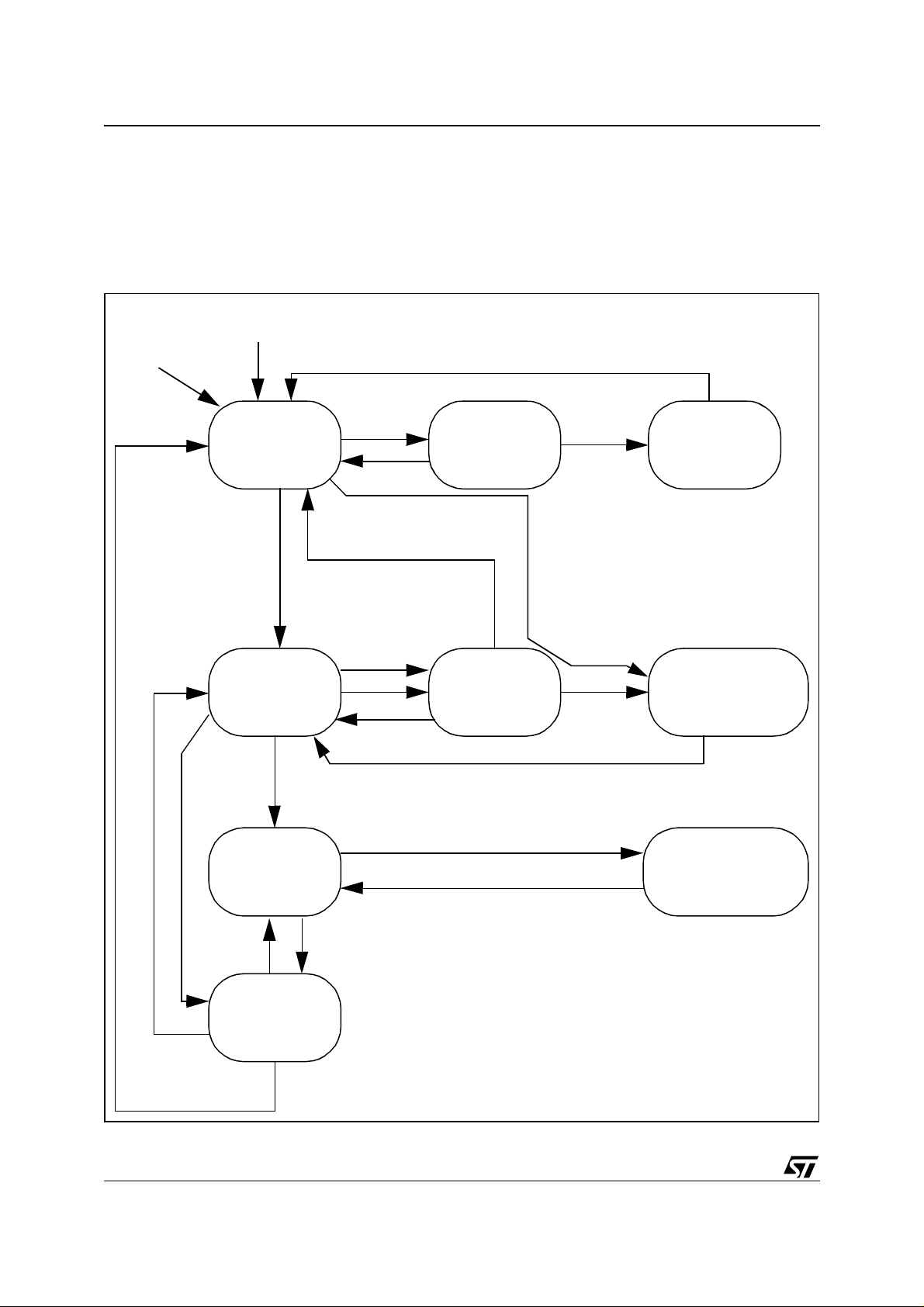
1.2 Power-Up, Initialization and Sleep mod e transitions
The following state-diagram illustrates the possible mode transitions inside the device.
As a prerequisite, a SPI-connection to the uC with the correct CRC-algorythms is required.
During the debug phase the NRES line can be forced high externally (connect to V1) to deactivate the startup
failure mechanis keeping V1 will alive.
Figure 3.
After POR, V1 up or externally forced reset
through low NRES, the STARTUP STATE is
entered
V1 Low
NRES Low
WAKEUP
STARTUP
V1 active
V2, V3, CAN off
WDC-ACK
Dependi g on th e value f rom the last
WDC-ACK, another one has to be
Writing to the WDCregister (WDC-ACK)
the NORMAL STATE is
entered.
written within the spec ified time frame
(SWDC[1:0]). A failure will activate
the STARTUP STATE
NORMAL MODE
WINDOW WDC
ACTIVE
WND SET
DISAR
SET
If during the last WDC-ACK WND has been set (after releasing
write lock , see d escription of Watc hdog Cont rol Register) th e Window wa tch do g is de act ivat e d, an d no uC sup erv ision is active.
NORMAL MODE
WINDOW WDC
DISABLED
The forced sleep mode is left upon wakeup through either CAN or edge on
WAKE. Appl ying a per manent wakeup ( i. e. bot h CAN-l ines domin ant) pr events V1 from being turned off (can be used during System debugging)
WAKEUP
Forcing NRES high externally, fail will not be incremented (Emulation)
STARTUP
t=320ms
FAILURE
fail = 7
RESET low
t=1ms
A missing ACK within 320ms will
initiate a STARTUP FAILURE
phase (RESET low).
WDC-FAIL
(fail ++)
If no WDC-ACK is recei ved within
seven retrials the voltage regulator
WDC-ACK
&
WDEN SET
The Window supervision can temporarily be deactivated for the time programmed during the
last WDC-ACK (WDT[3:0]). Upon rewriting
(WDC -AC K) or e xpiry of the time r, the NO R MAL
STATE is reentered.
V1 will be turned off by entering the
FORCED SLEEP state.
WDC-ACK
t=t
WIN2
WDC-OK
WINDOW
WATCHDOG
REFRESH
TIMEOUT | WDC-ACK
WDEN SET
TIMEOUT | WDC-ACK
FORCED SLEEP
V1 off
No Reset
TIMER
ACTIVEWDEN SET
(restart by double
WDC-ACK & WDEN)
Here the t imer ca n b e used to
generate time events (i.e.
wakeup uC from stop)
TIMER
ACTIVE
(restart by double
WDC-ACK & WDEN)
WAKEUP
&V1_UV
WAKEUP&V1_UV
10/35
WAKEUP
Programmed
SLEEP
V1 OFF
No Reset
DISAR
SET
Setti ng DI SAR ( see V ol t age Reg ul a t or Con t r ol R egi s te r ) Vol t ag e r e gu la t or V1 i s
turned off, and the output voltage is decreasing depending on the external load
and blocking capa citor .
Note, that during this transition no Reset will be generated (due to Debugmode).
Upon wakeup howewer NRES wil l be pulled low, if V1was below the programmable reset threshold (V1_UV).
Page 11

L4969
1.3 CAN Transceiver
– Supports double wire unshielded busses
– Baud rate up to 125KBaud
– Short circuit protection (battery, ground, wires shorted)
– Single wire operation possible (automatic switching to single wire upon bus failures)
– Bus not loaded in case of unpowered transceiver
The CAN transceiver stage is able to transfer serial data on two independent communication wires either deferentially (n ormal operation) or in case of a single wi re fault on the remaining li ne. The physical bitcoding is done
using dominant (transmitter active) and overwritable recessive states. Too long dominant phases are detected
internally and further transmission is automatically disabled (malfunction of protocol unit does not affect communication on the bus, "fail-sa fe" - mechanism). For low current consu mption during bus inactiv ity a sleep mode
is available. The operating mode can be entered from the sleep mode either by local wake up (
tection of a dominant bit on the CAN-bus (external wake up).
Ten different errors on the physical buslines can be distinguished:
1.3.1 Detectable Physical Busline Failures
N Type of Errors Conditions
Errors caused by damage of the datalines or isolation
µ
C) or upon de-
I CANH wire interrupted (tied to Ground or termination) Edgecount difference > 3
II CANL wire interrupted (floating or tied termination) Edgecount difference > 3
III CANH short circuit to V
IV CANL short circuit to GND (permanently dominant) V(CANL) < 3.1V & V(CANH)-V(CANL)
V CANH short circuit to GND (permanently recessive) Edgecount difference > 3
VI CANL short circuit to V
VII CANL shorted to CANH V(CANH) - V(CANL) < -3.25V after
Errors caused by misbehavior of transceiver stage
VIII CANH short circuit to VDD (permanently dominant) V(CANH) > 1.8V & V(CANH) -
IX CANL short circuit to VDD (permanently recessive) Edgecount difference > 3
Errors caused by defective protocol unit
X CANH, CANL driven dominant for more than 1.3ms
(overvoltage condition) V(CANH) > 7.2V after 32us
BAT
< -3.25V after 1.3ms
(overvoltage condition) V(CANL) > 7.2V after 32us
BAT
1.3ms
V(CANL) < -3.25V after 2.5ms
Not all of the 10 different errors lead to a breakdown of the whole communication.
So the errors can be categorized into 'negligible', 'problematic' and 'severe':
11/35
Page 12

L4969
1.3.2 Neg ligible Errors
1.3.2.1
Error I and II (CANH or CANL interrupted but still tied to termination)
Error IV and VIII (CANH or CANL permanently dominant by short circuit)
Transmitter
In all cases above data can still be transmitted in differential mode.
1.3.2.2
Error I and II (CANH or CANL interrupted but still tied to termination)
Error V and IX (CANH or CANL permanently recessive by short circuit)
Receiver
In all cases above data can still be received in differential mode.
1.3.3 Problematic Errors
1.3.3.1
Error III and VI (CANH or CANL show overvoltage condition by short circuit)
Transmitter
Data is transmitted using the remaining dataline (single wire)
1.3.3.2
Error III and VI (CANH or CANL show overvoltage condition by short circuit)
Receiver
Data is received using the remaining dataline (single wire)
1.3.4 Severe Errors
1.3.4.1
Error V and IX (CANH or CANL permanently recessive by short circuit)
Transmitter
Data is transmitted on the remaining dataline after short circuit detection
Error VII (CANH is shorted to CANL)
Data is transmitted on CANH or CANL after overcurrent was detected
Error X (attempt to transmit more than 10 successive dominant bits (at lowest bitrate specified)
Transmission is terminated (fail safe)
1.3.4.2
Error VII (CANH is shorted to CANL)
Receiver
Data is received on CANH or CANL after detection of permanent dominant state
Error IV and VIII (CANH or CANL permanently dominant by short circuit)
Data is received on CANH or CANL after short circuit was detected
Error X (reception of a sequence of dominant bits, violating the protocol rules)
Data is received normally, error is detected by protocol-unit
The error conditions is signaled issuing an error flag inside a dedicated register which is readable by the µC
through the serial interface. The information of the error type (I through X) is also stored into this register.
12/35
Page 13

L4969
1.4 Oscillator
A low power oscillator provides an internal clock. In sleep mode (Watchdog active) the output frequency is
250kHz, if the Watchdog function is not requested, the internal Oscillator is switched off.
In standby and operating mode the os cill ator is r unning at 1MHz, and can be c alibrated i n a r ange from -16% to
+16% using the
1.5 WatchdL4969og
A triple function programmable watchdog is integrated to perform the following tasks:
– Wakeup Watchdog:
When in sleep or standby mode the watchdog can generate a wakeup condition after a programmable period of time ranging from 80ms up to 45 minutes
– Startup Watchdog:
Upon V1 power-up or
ated periodically every 320ms for 2.5ms until activity of the
knowledge is received within 7 cycles (2.2sec). In this condition the device is forced into Sleep mode
until a Wakeup is detected and a startup cycle is reinitialized.
– Window Watchdog:
After passing the startup sequence, this watchdog request an ac knowledge by the
within a programmable timing fr ame, ranging from 2.5 ... 5ms up to 20 . .. 40ms. Upon a m issing or
misplaced acknowledge the Startup Watchdog is initialized.
µ
C-XTAL as a reference.
µC failure during SPI supervision (see SW-Wat chdog) a res et pulse is gener-
µC is detected (SPI sequence) or no ac-
µC via the SPI
1.6 Reset
1.6.1 Powe r- on Re set
Upon Power-on (VS > 3.5V), the internal reset forces the device into a predefined power-on state (see 1.1):
Standby #3:V1 on V2 off V3 off,CAN-Standby mode, ID-Filter disabled, Startup Watchdog active
With VS below 5V the regulator V1 will follow VS with minimum drop. The
µ
C retrieves a reset if V1 is dropping
below a programmable voltage level of either 4.5V (default) or 4.0V. The programmed state of the L4969 remains unchanged. The act. low Resetpulse duration is fixed internally by an open-drain output stage to 1ms.
However, this time can be externally extended by an additional capacitance connect between NRESET and
GROUND which is then charged by the internal pull-up of typ. 120K. Depending on the Reset-Input-Threshold
of the uC (U
C
= -tD / (120E3 ln(1-UTR/V1))).
EXT
To obtain a reset-pulse duration of t
), the reqired Capacitance for a typical tD can be calculated as follows:
TR
= 50ms with UTR/V1 = 0.5, a Capacitance of C
D
= -50E-3 / (120E3 ln
EXT
0.5) = 600nF is required.
Figure 4.
V1
120K
NRES
C
EXT
to Reset Input of uC
1.6.2 Un der volt age Rese t
Upon detection of a V1 voltage level below a programmable voltage level of either 4.5V (default) or 4.0V,the
NRES-pin is pulled low. Since this undervoltage detection is additionally sampled periodically every ms, the
NRES low time will be extended by up to 1 ms if V1 was low (V1
) at the sampling point (see below).
UV
13/35
Page 14

L4969
Figure 5.
1ms sampling
V1
UV
NRES
1.6.3 Reset signalling during Sleepmode
When entering the sleep mode by writing 1 to DISAR in the VRCR register, the Voltageregulators and their references will be deactivated to allow minimum current consumption. By removing the V1 reference, the outputvoltage is no longer supervised and thus NO reset will be generated.
Now two scenarios are possible (see statediagram in chapter 1.2):
1) Wakeup with V1 still above reset threshold: V1 will be reactivated and Normal mode is resumed
2) Wakeup with V1 below reset threshold: V1 will be activated, NRES will go low and remain low until V1 is
above reset threshold and Startup mode is entered.
The scenario 2 is the most critical when used with uC that do not have their own POR circuitry.
In this case V1 will ramp down with an unknown application state.
To guarantee a proper shut off of an uC without an internal POR circuitry the following mechanism can be utilized: The L4969 uses a bidirectional Reset to detect a possible Watchdog failure of the uC. If this failure condition is detected, NRES will be forced low for 1 ms (with activated timer) or until a wakeup condition occurs
(WDEN bit in WDC register reset, thus RC-oscillator will be switched off during sleep).
Two methods can be used to allow a proper sleep transition:
- With Timer (WDEN=1): immediately after setting DISAR the uC has to program its WDC to generate a failure
causing the L496 9 to detect a low level on NRES foll owed by an automatic 1m s pulse ex tension. If V1 is ramping
down slow, Cext has to be defined in a way, that NRES will stay below the input threshold of the uC until V1 is
in a safe level.
- Without timer (WDEN=0): same proc edure as above, bu t uC has to generate a R eset within 1 ms after WDEN
has been cleared. NRES will then stay low, until a wakeup condition occurs.
Figure 6.
.
DISAR
REF REG
R1
V1
R2
NRES
WDC
1ms
RC-Osc
C
EXT
uC
L4969
1.7 Identifier Fil ter
A 12-Bit CAN-ID-filter is implemented allowing wakeup via specific CAN-messages thus aiding the implementation of low power partial communication networks like standby diagnostics without the need to power-up the
whole network.
To guarantee the detection of the programmed Identifiers, the local RC-oscillator can be calibrated to allow the
programmable Bittime logic to extract the incoming stream with a maximum of tolerance over temperature deviation.
1.8 Groun d Shift Detection
14/35
Page 15

L4969
In case of single wire communication via CANH the signal to noise ratio is low. Detecting the local ground shift
can be used as an additional indicator on the current signal quality. The information of the integrated ground
shift detector will be refreshed upon every falling edge on TX and can be read from the CAN Transceiver Status
Register (CTSR).
It will be set, if V(CANH) < -1V, reset if V(CANH > -1V) at the falling edge of TX.
1.9 Thermal Protection
The device features three independent thermal warning circuits which moni tor the temperature of the V1 output,
the V2 output and the CAN_H and CAN_L drivers together with voltage regulator V3. Each circuit sets a separate overtemperature flag in a register which is read and writable by the serial interface. The overtemperature
flags cause an interrupt to the
enable registers. To enhance system security following strategy is chosen for thermal warning and shutdown:
– 3 independent warning flags are set at 140°C for V1, V2 and V3/CAN-Transceiver
– at 170°C V2 and V3 switched off
– at 200°C V1 is switched off
– V2 and V3 can be switched on again through the
– V1 can be switched on again at wake-up (Watchdog wake-up, CAN wake-up, external wake-up)
Note, that if no wakeup source is set for V1 a 1sec watchdog timeout will be established to enable a proper retry
cycle.
µ
C. The µC is able to switch V1, V2 and CAN drivers on and off through dedicated
µC
1.10 Serial Interface (SPI)
A standard serial p eripheral interfac e (SPI) is implemented to allow access to the internal register s of the L4969.
A total of 12 Registers with differen t datalengths ca n be directly read fr om or w ritten to, providi ng the req uested
address at the beginning of a dataframe. Upon every access to this interface, the content of the register currently
accessed is shifted out via SOUT. All operations are performed on the rising edge of SCLK.
If a frame is not completed, the interface is automatically reset after 1.5ms of SCLK idle time (auto timeout detection). If a message is corrupted ( additional or missi ng SCLK pulses), the appli cation softw are can detect thi s
by evaluating the returned value of the crc and force a communication gap of min 1.5ms to allow communicvation recovery. A corruption c an be caused during star tup of the uC and S PI initializ ation. The appli cation s hould
then wait at least 1.5ms after SPI init prior to starting the communication.
The dataframe format used described on the next page:
15/35
Page 16

L4969
1.10.1General Dataframe Format:
Figure 7.
SIN
7
SOUT ADR/CMD Datafield 1 (R) Datafield 2/CRC (R)
SCLK
99AT0015
ADR/CMD
Datafield 1 (W/R)
0
15
0715
8823
Datafield 2/CRC (W/R)
23
15
15
Data is sampled on the rising edge of the clock and SOUT will change upon SCLK falling. SOUT will show a
copy of SIN for the Address/ C ommand field for initial data path checks. Independent of the command state,
SOUT will show the content of the register addressed. SIN contains either data to be written or arbitrary data
for all other operations. The transaction will be terminated with four bit of data followed by a 4-Bit wide CRC
(Cyclic Redundancy Check) as a result of either SIN related data or calculated automatically on data returned
via SOUT. Here the
µ
C has to provide the cor rect sequenc e in order to get the write command acti vated ins ide.
A CRC-failure is signall ed v ia N INT. For r eturned data the C RC c an als o be used to verify a succ essful tr ansfer.
1.10.2 Address/Command Field
Figure 8.
70
C0
Frame start sequence
always has to be
transmitted as 0 1
ADR310
ADR2 ADR1
Addressfield specifying
the Control/Status word
to be accessed
ADR0 C1
SPI command:
00: Read register
01: C le a r IFR
10: illegal command
11: Write register
The Address/Command field starts with a 2-Bit start sequence consisting of ‘01’. Any other sequence will lead
to a protocol error signalled via the NINT. The addressfield is specifying the register to be accessed. The SPI
command flags all ow in additi on to the normal r ead/write operation to clear the Interrupt flag regis ter after read.
16/35
Page 17

1.10.3 Datafield #1
Figure 9.
L4969
D7
D6
D5
D4 D3
D2
D1 D0
Lower 8 Bit of 12 Bit data
SIN: Data to write
99AT0017
SOUT: Data currently in selected register
Datafield #1 contains either the lower 8 bits of a 12-Bit frame or the complete byte of an 8-Bit transfer.
Note, that SOUT is always show ing the content of the register cur rently acc essed a nd not a c opy of SIN as during the Address/Command field.
1.10.4 Datafield #2/CRC
Figure 10.
D11
D10 D9 D8
CRC3 CRC2 CRC1 CRC0
Upper 4 Bit of 12 Bit data (Zero if 8 Bit data)
CRC Check sequence
to be appended to tranferred data
Note that upon CRC check failure
no write operation will be performed
SIN: Data to write
SOUT: Data currently in selected register
99AT0018
SIN: CRC of SIN sequence
SOUT: CRC of SOUT sequence
Datafield #2 contains either the upper four bits of a 12-Bit frame or zeros in case of an 8-Bit transfer. This field
is followed by a four bit CRC sequence that is calculated based upon the polynom 0x11h (17 decimal). This
sequence is simply the remainder of a polynomial division performed on the data previously transferred. If the
CRC appended to the SIN sequence fails, any writing will be disabled and an error is signalled via NINT. Another
remainder is cal culated on the SOUT stream and appended accor ding ly t o all ow the appli cation software to validate the correctness of incoming data. To aid evaluation, the CRC checking can be turned off by writing arbitrary data with a valid CRC to address 15. CRC-checking will be reenabled upon another operation of this kind
(Toggled information).
17/35
Page 18

L4969
1.11 Memory Map
Table 5. L4969 Memory Map
ADR Group MSB D10 D9 D8 D7 D6 D5 D4 D3 D2 D1 D0
0 VRCR
1CTCR
2GPTR
3 RCADJ
4WDC
5GIEN
6IFR
7CTSR
8ID01
9ID23
10 BTL
11 NAV
12 NAV
13 NAV
14 TEST
15 SYS
Undefined
Register Memory
ESPI ISET IRES UV23 UVVS OVT3 OVT2 OVT1 WKE WKC WKW WKIF
RES RES RES GSH EX EVIII EVII EVI EIV EIII EII EI
A11 A10 A01 A00 B11 B10 B01 B00 C11 C10 C01 C00
D11 D10 D01 D00 E11 E10 E01 E00 F11 F10 F01 F00
PS23 PS22 PS21 PS20 PS13 PS12 PS11 PS10 TD3 TD2 TD1 TD0
T11 T10 T09 T08 T07 T06 T05 T04 T03 T02 T01 T00
Undefined Register Memory NCRC STAT WNDF STF OTF UCF WAKE NPOR
EUV3 EUV2 RTC0 TRC RES ENV3 ENV2 DISAR
ACT TXEN RES RES RES LP2 LP1 LP0
RES RES RES RES TM1 TM0 TMUX TEN
CG1 CG0 PGEN SIGN ADJ3 ADJ2 ADJ1 ADJ0
WDEN WND SWT1 SWT0 WDT3 WDT2 WDT1 WDT0
ISET IRES EUV EOVT EEW ECW EWW EIFW
Undefined
Register Memory
The memory space is divided up into 16 different registers each being directly accessible using the SPI.
Each register contains specific information of a functional group.
In general al reserved bitpositions (‘RES’) have to be written with ‘0’.
Undefined bits are read as ‘0’ and cannot be overwritten.
In addition there is one register (CTSR) being read only, thus any write attempt will leave the register content
unchanged.
Certain interlock mechanism exist to prevent unwanted overwriting of important functions i.e. voltage regulators
or oscillator adjustments. These mechanisms are described with the functions of these registers.
*1) “shorted to ...”
18/35
Page 19

L4969
2 CONTROL AND STATUS REGISTERS
The functionality of the device can be observed and controlled through a set of registers which are read and
writable by the serial interface.
2.1 ADR 0: VRCR Voltage Regulator Control Register
Figure 11.
D7 D0
EUV2EUV3 ENV3 ENV2 DISAR
RTC0
TRC
RES
Has to be
Enable undervoltage
written as ‘0 ’.
detection on
Regulator #2 and #3
(see note below)
Set reset threshold value to 4.0V
Default value is ‘0’ (4.5V)
Enable Regulator #2 tracking option
to have V2 following V1 with constant offset
Default value is ‘0’ (disabled)
Enable Regulator #3 .
V3 will be activated by either setting ENV3 or
upon enabling of the CAN Lineinterface
Default value is ‘0’ (dis a ble d)
This bit will be automatically reset upon
Overtemperature from CANIF or Regulator #3
Disable all Regulators (Go to Sleep)
Note, that at least one Wakeup Source
without a pending wakeup is required
to enable access.
This bit will be automatically set upon
the system failures Overtemperature V1
or watchdog startup failure.
Note, that no reset will be generated
from low V1 during Sleep mode transition
The Reset line has to be forced low
externally, or through a window failure
DISAR will be cleared upon a valid
wakeup signal which is either defined
in GIEN or is forced to WAKE or CAN
after a system fail ure
Enable Regulator #2.
Default value is ‘0’ (disabled)
This bit will be automatically reset upon
Overtemperature at Regulator #2.
Note, that due to the large initial charging current of the output capacitors,
the activation of V2 AND V3 within the same command is not recommended
also leaving ENV2 or ENV3 set when setting DISAR can therefor not be
recommended (after wakeup V1 AND V2 or V3 would be turned on)
TRC
DISAR
REF
V1 V3
Note, that when using the Undervoltage-detecti on, EUV2 and EUV3 have to be activated
DISAR
& ENV2
(DISAR
ACT) & T SDV3
V2
V3 will be activated upon VRCR.ENV3 or
CCTR.ACT without pending thermal shutdown
AFTER
& ENV3 |
V2 or V3 have
been turned on and settled (t > 1ms). Otherwise unwanted undervoltage can be detectected dur ing turn on of
the corresponding voltage regulator.
19/35
Page 20

L4969
2.2 ADR 1: CTCR CAN-Transceiver Control Register
Figure 12.
D7 D0
RESTXENACT
RES RES
LP2
LP1 LP0
Standby-m ode control (V1 only, see 1.1)
CAN-Trans ceiver application control
0X : Standby / Sleep
reduce Osc-fr equency to 250KHz
enabl e Auto-Osc-Off
10 : Receive only mode A (Readback TX, if not EX)
11 : Normal Operat ion
Note, that TXEN is automatically reset upon
occurence of EX (TX permanent dominant)
and has to be reprogrammed after problem
correction to enter normal mode.
Reserved bits (‘RES’) have to be written as ‘0’.
Three basic operating modes are available using different logic combinations on ACT and TXEN. Each of these
modes in conjunction with other inputs has its unique combination of parameters inside the specification:
Table 6. Operating Modes of the CAN Lineinterface
Input Signals Output Signals
ACT TXEN TX CANH CANL V3 Mode RTL RTH CANH CANL RX
0 X X RTH RTL ON Standby V
1 0 1/0 RTH RTL ON RXonly V
1 0 1 RTL ON RXonly V
1 0 1 RTH ON RXonly V
1 1 1 RTH RTL ON Normal V
1 1 0 RTH RTL ON Normal V
1 1 1 RTL ON Normal V
1 1 1 RTH ON Normal V
*1
11
0
1X1
1X1
RTH RTL ON Error X V
VDD
VS
*1
*1
RTL ON Error
VII, VIII
RTL ON Error
EIII, VII, VIII
1 X 1 GND x 3 ON Error
EI_V
1X1 x 3VDDON Error
EII_IX
1X1RTH
1X1RTH
1X1
CANL
*1
VS
GND
CANH
*1
*1
*1
ON Error
EVI
ON Error
EVII, EIV
ON Error
EVII
ISRC GND ON OFF CANH
ISRC GND ON OFF CANH
ISRC GND ON OFF CANH
V
V
V
V
GND OFF OFF 1
BAT
GND OFF OFF TX
DD
GND OFF OFF
DD
GND OFF OFF
DD
GND ON ON 1
DD
GND VDD GND 0
DD
GND ON ON
DD
GND ON ON
DD
GND OFF OFF 1
DD
ISRC OFF ON CANL
DD
ISRC OFF ON CANL
DD
GND ON ON
DD
GND ON ON
DD
20/35
Page 21

2.3 ADR 2: GPTR Global Parameter and Test Register
Figure 13.
D7 D0
L4969
RES
This register is to be used for testpurpose only, all bits have to remain ‘zero’
2.4 ADR 3: RCADJ RC-Oscillator Adjust register
Figure 14.
RES RES
RES
TM1 TM0 TMUX TEN
D7
CG1 CG0 PGEN ADJ4 ADJ3 ADJ2 ADJ1 ADJ0
0: 0%
1: +16%
0: 0%
1: -8%
0: 0%
1: -4%
0: 0%
1: -2%
Program enable (read only)
Bit will be set after 'Finish cycle measurement',
and reset after register write
D0
0: 0%
1: -1%
RC Oscillator
Frequency Adjust
default value 10000
Note, that programming
is only enabled with PGEN set
Test cycle request
A low pulse on NINT
for a fixed period
of time can be requested
for XTAL synchronization
99AT0022
During normal operation the µC can set CG1 and CG0 to ‘01’ to force a 200Hz rectangular waveform on NINT
with 50% duty cycle. Note, that all other pending interrupts have to be cleared before.
After the XTAL driven timer of the
CG1 and CG0 have to be set to ‘10’ to disable the adjustment cycle on NINT. From the deviation calculated by
the
µ
C, the correction factor of the RC-oscillator -15% to + 16% can be reprogrammed with CG1 and CG0 set
to ‘00’ or ‘11’. (‘11’ can be used to indicate that calibration has already been performed).
Note, that overwriting this register is only valid, if the cycle measurement was started and terminated properly.
This can be tested by evaluating PGEN either prior to or during correction (Read back via SOUT).
Note also, that any write to the W DC register w ill reset the timer a nd thus reset the phase of the testcycle. Therefore a cyclic access to the window watchdog during the pulsewidth measurement has to be avoided and the
timer watchdog to be used instead (i.e. 1sec)
µ
C calculated the relative cycle time and the corresponding deviation,
00: No request (Adjustment disabled)
01: 2.5ms low cycle on NINT (repetitive)
10: Finish cycle measurement
11: No request (Adjustment disabled)
21/35
Page 22

L4969
Figure 15.
State transition during oscillator calibration
CG=01
“No Request”
Watchdog and Interrupt
has to be disabled
“2.5ms cycle
on NINT”
Start time measurement
at rising edge
CG=10 CG=00
2.5 ADR4: WDC Watchdog Control Register
Figure 16.
D7 D0
SWT0 WDT3SWT1WNDWDEN WDT2 WDT1 WDT0
Disable
Window Watchdog,
only allowed with
PGEN set, see
previous table
for Osc adjust
Enable Wakeup Watchdog,
Window Watchdog will be
automatically deactivated
until wakeup watchdog expires
Reserved bits (‘RES’) have to be written as ‘0’.
Software Window Watchdog
timing configuration
00 : 2.5 - 5ms
01 : 5 - 10ms
10 : 10 - 20ms
11 : 20 - 40ms
“Finish Cycle” “Update ADJ”
CG=11
Calculate
Offset
Watchdog and Interrupt can be enabled
Write offset
Wakeup Watc hdog
timing configuration
0000 : 80ms
0001 : 160ms
0010 : 320ms
0011 : 640ms
0100 : 800ms
1000 : 1sec
1001 : 2sec
1010 : 4sec
1011 : 8sec
1100 : 45min
The Startup Watchdog is not programmable and will always generate a 1.0ms low cycle on NRESET followed
by a 320ms high cycle until an Acknowledgment will occur. If no Acknowldege is received after the 7th cycle,
the device will automatically be forced into Sleep mode.
Acknowledgment and Reset of Startup and Window Watchdog is automatically performed by overwriting
(or rewriting) this register.
Note, that with WDEN set, a cyclic setting of IFR.WKW after the programmed Wakeup time will occur.
2.5.1 Watchdog configuration:
22/35
Page 23

L4969
Figure 17.
POR
NRESET
forced low
externally
Wakeup
Prog
Sleep
Ack
Note: WR, writing to this address, will restart the timer
After power-on-reset of VS and V1 or wakeup from Sleep or NRESET being forced low externally, the Startup
Watchdog is active, supervising the proper startup of the V1 supplied uC. Upon missing SPI write operation to
the WDC register after 7 reset cycles (1ms active, 320ms high) the Sleep mode is entered.
Leaving the forced Sleep mode will be automatically performed upon wakeup via CAN, an edge on WAKE or
upon device powerup.
After successful startup, the W indow Watchdog supervision is activated, meaning, that the uC has to send an
acknowledge within a predefined, programmable w i ndow.
Upon failure, a reset is generated and the Startup Watchdog is reactivated.
If the Timer func tion is requ ested, t he window watchdog is deactivated until expiry o f the wakeup tim e, or rewriting of this register. Note, that any write to this register will reset the timer.
Ack
ExtWake
Startup
Wd
Window
Wd
CAN-Wake
missing Ack
(after 350ms)
missing
Ack
Timeout
WR
WR & WDEN
Forced
Sleep
Wakeup
Timer
2.5.2 Startup
Figure 18.
V1
1ms
NRESET
Startup Acknowledgement via SPI within 320ms
NRESET
Startup Acknowledgemen t via SPI within 640ms
NRESET
No Startup Acknowledgement via SPI within 2.3s (De vice will enter Sleep mode)
After powerup, the L4969 is expec ting the uC to send an ac knowledgement w ithin a predefined segmented timing frame of 7 x 320ms. A missing acknowledgement until after the 2.3s will force the device into sleep mode
until either external or CAN wakeup or POR cause a restart of the sequence above.
2.5.3 Window Watchdog
23/35
Page 24

L4969
Figure 19.
2,5 .. 20ms
50%
Early (late) Acknowlede supervision
5 .. 40ms
Early (late) Acknowlede supervision
Acknow ledge is restarting Window
After successful acknowledgement of the Startup sequence, the Window watchdog is automatically activated
and controlling proper uC activity by super vising an incoming acknowledge to ly within a predefined programmable window. Upon every acknowledge the watchdog is restarting the window.
24/35
Page 25

2.5.4 Wakeup Watchdog
Figure 20.
Window Wd Window WdTimer (80ms .. 45min)
L4969
restart tim e r
at any time
writing WDC twice
Timeout and resume Window Wd
NINT
Ack Window &
Start Timer
Interrupt active upon timeout (via GIEN)
If the Timer is activated during N ormal mode by setting WDEN in WDC, an “acknowledge-free” sequence is
started for a predefied programmable time. Window Watchdog activity is resumed after expiry of the timer.
To be able to detect the timeout, the corresponding interrupt enable must be set in GIEN.
This mode can also be used to allow a bootstrap loader mode with longer execution times than the maximum
specified window. Correct s tartup of this load er i s safely detected upon mi ssing r esponse following the timeout.
The timer can always be restarted by rewriting WDEN twice in WDC with a new timing.
25/35
Page 26

L4969
2.6 ADR5: GIEN Global Interrupt Enable Register
Figure 21.
D7 D0
EOVT EEWEUVIRESISET ECW EWW EIFW
Enable Interrupt
upon CAN error
detection
Enable CAN
wakeup / Interrupt
Enable Interrupt
upon CAN error
recov ery
Enable
Interrupt
upon VS / VREG
Undervoltage
Enable Interrupt
upon Overtemp.
Warning
Enable Wakeup / Interrupt
via edge on WAKE
Enable Identifier
based wakeup / Interrupt
Enable Wakeup,/ Interrupt
via Watchdog
2.7 ADR6: IFR Interrupt Flag Register
Figure 22.
D11 D0
ESPI ISET IRES UV23
CAN Linefailure
detected (ISET)
remov e d (IRE S )
CRC- / Format
Error or SCL KTimeout detected
by SPI (non maskable)
UVVS
VS < 7.2V
detected
V2 or V3
Undervoltage
OVT1 : T(V1) > 140degC
OVT2 : T(V2) > 140degC
OVT3 : T(V3) > 140degC
OVT3
Overtemperature
Warning level reached
OVT2
OVT1
WKE
Signal edge
on W AKE
dete cte d
W ak eup condition
via CAN detected
Watchdog timeout
detected
WKWWKC
Identifier passed
CAN ID-Filter
WKIF
Reserved bit (‘RES’) has to be written as ‘0’.
Except ESPI all bits in this register are maskable in GIEN. Any mask ed bit will force NINT low until the register
content is reset (either explicitly or by SPI ‘clear register).
26/35
Page 27

2.8 ADR7: CTSR CAN Transceiver Status Register
Figure 23.
D11 D0
RES RES RES GSH EI_VEII_IXEIIIEIVEVIII EV II EVIEX
L4969
CANH < -1V
at falling edge TX
TX permanent
dominant detected
(TXD = ‘0’, t > 1.3ms)
CANH permanen t
dominant detected
(CANH > 1.8V, t > 1.3ms)
CANL short
circuit to VS
detected
(CANL > 7.2V ,
t > 32us)
CANL permanent
dominan t de tec t ed
(CANL < 3.1V,
t > 1.3ms)
Short circuit CANH to CANL detected
(CANH - CANL > -3.25V, t > 1.3ms)
CANH short
circuit to VS
detected
(CANH > 7.2V,
t > 32us)
Reserved bit s (‘RE S ’) are al w ays read as ‘0’
Note, that this register i s read only and only provides the unlatched i nformation on current bus errors.
Single wire
communication
detected
(edge co unt
difference > 3)
EI_V : CANH off
EII_IX : CANL off
27/35
Page 28

L4969
2.9 ADR 8 and 9: ID01, ID23 Identifier Filter Sequence Select Register
Figure 24.
SEGA SEGB SEGC SEGD SEGE SEGF
00
A00
A01
A10
A11
SOF
ID10 ID9 ID8
4/2
Demux
11
ID7
ID6 ID5
ID4
ID3
ID2 ID1
00
F00
F01
F10
F11
ID0
Demux
RTR
4/2
11
99AT0028
PASS
Identifier of CAN Frame can be divided up into 6 segments numbered from ‘A’ to ‘F’.
For each segment a filter regis t er is im plemented, enabl ing different pass func tions on ever y two bit w ide block.
Segments A through C (ID01) are located at ADR 8 with MSB ‘C11’
Segments D through F (ID23) are located at ADR 9 with MSB ‘F11’
Note, that clearing a complete segment disables the whole filter.
SEGE
SEGF
01 01 01
01 11 01
Valid sequence
for each segment
SEGA: A10, A00
SEGB: B01
SEGC: C01, C00
SEGD: D10, D01
ID bits to be set
0101
0010 ID01: 0011 0010 0101
0011
0110
Examples:
Identifiers to pass:
SEGD
10 01 00
10 01 01
00 01 01 10 00 10
SEGE: E11, E01, E00 1011 ID01: 0110 1011 0110
SEGA
SEGC
SEGF: F10, F01
0011
SEGB
28/35
Page 29

2.10 ADR 10: BTL Identifier Filter Bittimelogic Control Reg ister
Figure 25.
D11 D0
L4969
PS23 PS22 PS21 PS2 PS13 PS12 PS11 PS10
Phasesegment 2
length configuration
t
= 1us * PSEG2 t
PSEG2
Phasesegment 1
length configuration
= 1us * (1 + PSEG1)
PSEG1
Bittime synchronization mechanism
t
PSEG1
TD3
TD2 TD1
Dominant to Rezessive
bitlength difference control
td = t
t
PSEG2
dom
- t
TD0
rez
t = 1u
Sample Point
99AT0030
The total bitlength equals the sum of 1 + PSEG1 + PSEG2 in units of µs.
The location of the sampling point is determined by the length of PSEG1.
At the start of frame (initial recessive to dominant edge) the bitlength counter is reset.
Upon every signal edge the counter will be lengthened or shortened according to location of the transition wi thin
the programmed boundaries of PSEG1 or PSEG2. If the edge lies within PSEG1 additional cycles are inserted
in order to shift the sampling point to a safe location after the settling of the input signal. If the signal transition
is located within PSEG2, this segment will be shortened accordingly with the goal of the next edge to lie at the
beginning of PSEG1.
The amount of cycles one segment is lengthened or shortened is determined by the type of edge (rec -> dom
or dom -> rec) and the programming of TD: The resynchronization jump width will be either set to ‘1’ (dom ->
rec edge) or to 1 + TD (rec -> dom edge).
Note, that the length of one timequanta depends on the offset of the on chip RC-oscillator and therefore on the
accuracy of calibration (see register RCADJ (ADR 3) for details on frequency correction)
29/35
Page 30

L4969
2.11 ADR 15: SYS System Status Register
Figure 26.
D7 D0
STF
CRC-Checking
disabled
OTFWNDFSTATNCRC UCF W AKE NPOR
Cold Start
after low VS
Reserved
status flag
(test only)
Warm start
Warm start
after V 1
Overtemp failure
Warm start
after leaving
prog. Sleep mode
after failure of
Window watchdog
Warm start
after 7 m i ss i n g
Ack during Startup
Warm start
after < 7 missing
Ack during Startup
The lower 6 bit of this register can be used to analyze the reason of startup (after NRESET low). This information
is valid until the first Watchdog-Acknowldge, and will then be reinitialized to 000001.
30/35
Page 31

3 INTERRUPT MANAGEMENT
Figure 27.
L4969
D11 D0
ESPI ISET IRES UV23
IFR
WKIFWKWWKCWKEOVT3 OVT2 OVT1UVVS
EUVIRESISET ECW EWW EIFW
EOVT
EEW
D7 D0
GIEN
NINT
All Interrupt flags (in IFR) except ESPI can be masked in the global interrupt enable register (GIEN).
An Interrupt will be signalled by NINT going low until either the corresponding ma sk or the flag itself will be reset
by the applicati on software. A n auto reset functi on is avai lable for IFR, allow ing to remove all i nter rupt flags after
reading their state (see SPI).
31/35
Page 32

L4969
4 REMARKS FOR APPLICATION
Figure 28. General circuit connection diagram
Thermal
VS
Supervision
*
10u
47n
Standby Supply
& Adjustable
RC-Oscillator
V2
V1
*
47n
Peripheral
Supply
10u
33u
*
47p
*
47n
Programmable
Timer
Wakeup & Interrupt
Detection
WAKE
V3
RTH
CANH
CANL
CAN
Transceiver
Groundshift
Detection
SPI
120K
NRES
NINT
SCLK
SOUT
SIN
RX
TX
*
47n
10u
opt
µC
*
47p
99AT0032
C* ceramic C close to pin recommended for EMI
32/35
RTL
ID-Filter
GND
Page 33

L4969
DIM.
MIN. TYP. MAX. MIN. TYP. MAX.
A 2.35 2.65 0.093 0.104
A1 0.1 0.3 0.004 0.012
B 0.33 0.51 0.013 0.020
C 0.23 0.32 0.009 0.013
D 12.6 13 0.496 0.512
E 7.4 7.6 0.291 0.299
e 1.27 0.050
H 10 10.65 0.394 0.419
h 0.25 0.75 0.010 0.030
L 0.4 1.27 0.016 0.050
K 0˚ (min.)8˚ (max.)
mm inch
OUTLINE AND
MECHANICAL DATA
SO20
B
e
D
1120
110
L
h x 45˚
A
K
A1
C
H
E
SO20MEC
33/35
Page 34

L4969
DIM.
MIN. TYP . MAX. MIN. TYP . MAX.
mm inch
A 3.6 0.142
a1 0.1 0.3 0.004 0.012
a2 3.3 0.130
a3 0 0.1 0.000 0.004
b 0.4 0.53 0.016 0.021
c 0.23 0.32 0.009 0.013
D (1) 15.8 16 0.622 0.630
D1 9.4 9.8 0.370 0.386
E 13.9 14.5 0.547 0.570
e 1.27 0.050
e3 11.43 0.450
E1 (1) 10.9 11.1 0.429 0.437
E2 2.9 0.114
E3 5.8 6.2 0.228 0.244
G 0 0.1 0.000 0.004
H 15.5 15.9 0.610 0.626
h 1.1 0.043
L 0.8 1.1 0.031 0.043
N 8˚ (typ.)
S 8˚ (max.)
T 10 0.394
(1) “D and E1” do not include mold flash or protusions.
- Mold flash or protusions shall not exceed 0.15mm (0.00 6”)
- Critical dimensions: “E”, “G” and “a3”.
OUTLINE AND
MECHANICAL DATA
Weight:
1.9gr
JEDEC MO-166
PowerSO20
E2
NN
a2
b
h x 45
DETAIL A
e3
H
D
T
110
e
1120
E1
A
DETAIL B
PSO20MEC
R
lead
a3
Gage Plane
BOTTOM VIEW
E
DETAIL B
0.35
S
D1
L
c
a1
DETAIL A
slug
- C -
SEATING PLANE
GC
(COPLANARITY)
E3
0056635
34/35
Page 35

L4969
Information furnished is believed to be accurate and reliable. However, STMicroelectronics assumes no responsibility for the consequences
of use of such information nor for any infringement of patents or other rights of third parties which may result from its use. No license is granted
by implic ation or oth erwise unde r any patent or patent r i ghts of STMi croelectroni cs. Speci fications me ntioned in this publicat ion are subj ect
to change without notice. This publication supersedes and replaces all information previously supplied. STMicroelectronics products are not
authorized for use as crit i cal components in life support devices or sy st em s without express writt en approval of STMi croelectronics.
The ST logo is a registered trademark of STMicroelectronics
© 2003 STMic roelectronic s - All Rights Reserved
Austra lia - Brazil - Canada - China - F i nl and - France - G erm any - Hong Kong - India - Israel - Italy - Japan -M alaysia - Ma l ta - Morocco -
Singap ore - Spain - Sw eden - Switzerl and - United Ki ngdom - Unit ed S tates.
STMicroelectronics GROUP OF COMPANIES
http://www.s t. com
35/35
 Loading...