

Page 1
2.5APOWER SWITCHING REGULATOR
2.5AOUTPUTCURRENT
5.1V TO40V OPUTPUTVOLTAGERANGE
PRECISE(±2%) ON-CHIPREFERENCE
HIGH SWITCHING FREQUENCY
VERYHIGH EFFICIENCY (UP TO 90%)
VERYFEW EXTERNALCOMPONENTS
SOFT START
INTERNALLIMITINGCURRENT
THERMALSHUTDOWN
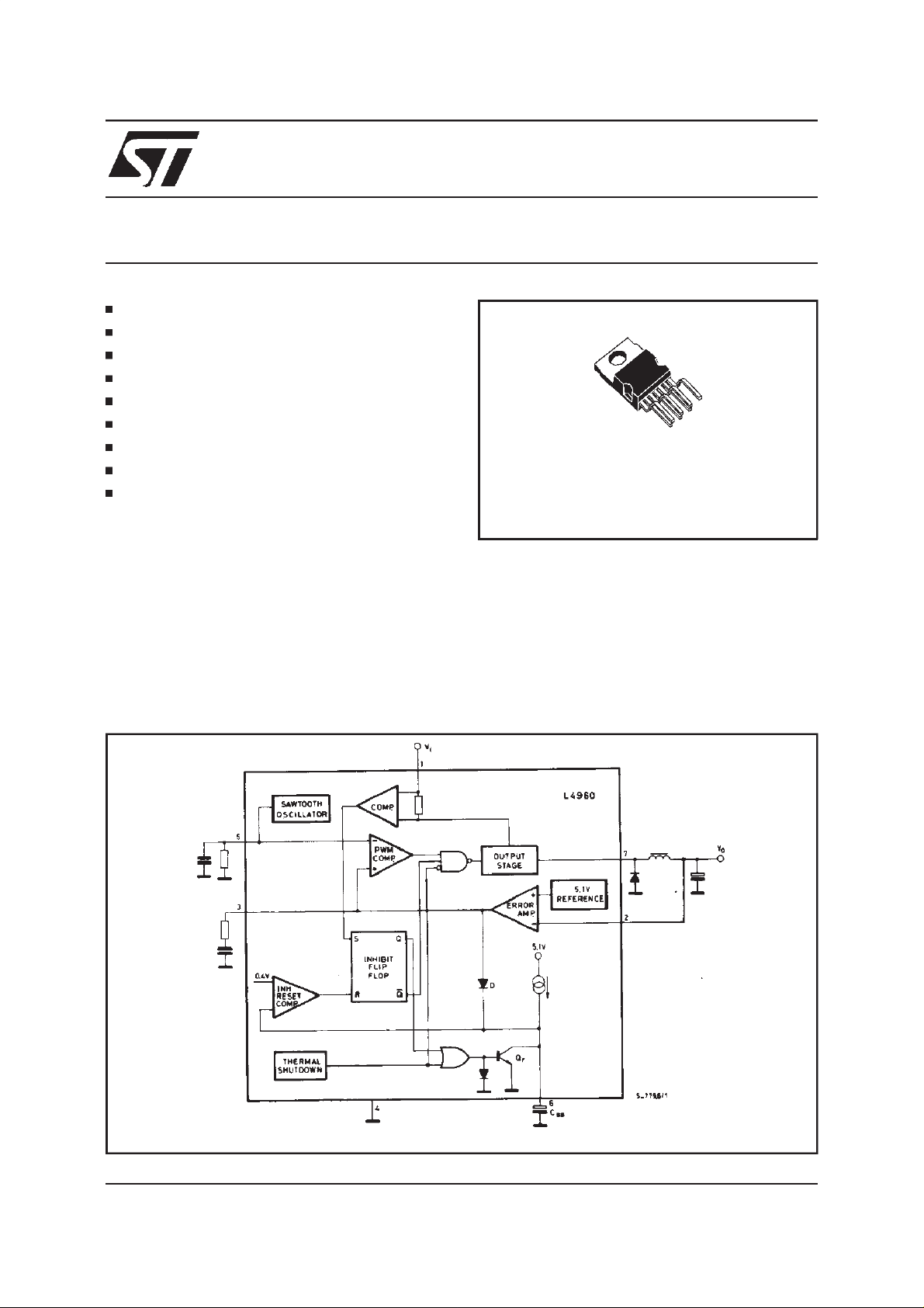
L4960
HEPTAWATT
ORDERING NUMBERS: L4960(Vertical)
L4960H(Horizontal)
DESCRIPTION
TheL4960 is a monolithicpower switching regulator delivering2.5Aat a voltage variable from 5V to
40V in step down configuration.
Featuresofthe device includecurrentlimiting,soft
start,thermal protectionand 0 to 100% dutycycle
for continuousoperationmode.
BLOCKDIAGRAM
TheL4960is mountedina Heptawattplastic power
package and requires very few external components.
Efficient operation at switching frequencies up to
150KHzallows a reductionin the size and cost of
externalfiltercomponents.
June 2000
1/16
Page 2
L4960
PIN CONNECTION
(Top view)
ABSOLUTE MAXIMUM RATINGS
Symbol Parameter Value Unit
V
V
1-V7
V
V
3,V6
V
P
T
,T
j
Input voltage 50 V
1
Input to output voltage difference 50 V
Negative output DC voltage -1 V
7
Negative output peak voltage at t = 0.1µs; f= 100KHz -5 V
Voltageat pin 3and 6 5.5 V
Voltageat pin 2 7V
2
Pin 3 sink current 1 mA
I
3
I
Pin 5 source current 20 mA
5
Power dissipation at T
tot
Junction and storage temperature -40 to150 °C
stg
case
C15W
≤90°
PIN FUNCTIONS
N° NAME
1 SUPPLYVOLTAGE Unregulated voltage input. An internal regulator powers the
internal logic.
2 FEEDBACK INPUT The feedback terminal of the regulation loop. The output is
connected directly to this terminal for 5.1V operation; it is
connected viaa divider for higher voltages.
3 FREQUENCY
COMPENSATION
A series RC network connected between this terminal and
ground determines the regulation loop gain characteristics.
4 GROUND Common ground terminal.
5 OSCILLATOR AparallelRC network connected tothis terminal determines the
switching frequency.
6 SOFT START Soft start time constant. A capacitor is connected between this
terminal and ground to define the soft start time constant. This
capacitor also determines the average short circuit output
current.
7 OUTPUT Regulator output.
FUNCTION
2/16
Page 3
THERMALDATA
Symbol Parameter Value Unit
R
th j-case
R
th j-amb
Thermal resistance junction-case max 4
Thermal resistance junction-ambient max 50
L4960
C/W
°
C/W
°
ELECTRICAL CHARACTERISTICS
(Refer to the test circuit, T
=25°C, Vi= 35V, unless otherwise
j
specified)
Symbol Parameter Test Conditions Min. Typ. Max. Unit
DYNAMICCHARACTERISTICS
V
∆ V
∆
V
∆
∆
V
I
I
Output voltage range Vi= 46V Io=1A V
o
V
Input voltage range Vo=V
i
Line regulation Vi= 10V to 40V Vo=V
o
V
Load regulation Vo=V
o
Internal reference voltage
ref
ref
ref
Vi= 9V to46V Io= 1A 5 5.1 5.2 V
to 36V Io= 2.5A 9 46 V
=1A 15 50 mV
refIo
Io= 0.5A to 2A 10 30 mV
ref
(pin 2)
V
Average temperature
ref
coefficient of refervoltage
T
Dropout voltage Io= 2A 1.4 3 V
d
Maximum operatingload
om
current
Current limiting threshold
7L
(pin 7)
T
=0°C to125°C
j
=1A
I
o
Vi= 9V to46V
V
o=Vref
to 36V
Vi= 9V to46V
o=Vref
to 36V
V
2.5 A
0.4 mV/°C
3 4.5 A
40 V
I
SVR Supply voltage ripple
Input average current Vi= 46V; outputshort-circuit 30 60 mA
SH
Efficiency f = 100KHz V
η
=2A Vo= 12V 85 %
I
o
V
=2V
∆
rejection
fripple
V
o=Vref
i
= 100Hz
rms
o=Vref
50 56 dB
Io = 1A
75 %
f Switching frequency 85 100 115 KHz
∆ f
∆
∆
∆
f
max
Voltagestability of
switching frequency
V
i
f
Temperature stability of
switching frequency
T
j
Maximum operating
Vi= 9V to46V 0.5 %
Tj=0°C to125°C1%
Vo=V
ref
Io= 2A 120 150 KHz
switching frequency
T
Thermal shutdown
sd
junction temperature
150
C
°
3/16
Page 4
L4960
ELECTRICAL CHARACTERISTICS
(continued)
Symbol Parameter Test Conditions Min. Typ. Max. Unit
DC CHARACTERISTICS
I
Quiescent draincurrent 100% dutycycle
1Q
pins 5and 7 open
V
= 46V
i
0% duty cycle 15 20 mA
-I
Output leakagecurrent 0% duty cycle 1 mA
7L
30 40 mA
SOFT START
I
6SO
I
Source current 100 140 180
Sink current 50 70 120
6SI
ERRORAMPLIFIER
V
V
I
High level output voltage V2= 4.7V I3= 100µA 3.5 V
3H
Low level output voltage V2= 5.3V I3= 100µA 0.5 V
3L
Sink output current V2= 5.3V 100 150 µA
3SI
A
µ
A
µ
-I
G
Source outputcurrent V2= 4.7V 100 150
3SO
I
Input bias current V2= 5.2V 2 10 µA
2
DC openloop gain V3=1Vto3V 46 55 dB
v
OSCILLATOR
-I
Oscillator sourcecurrent 5 mA
5
A
µ
4/16
Page 5
L4960
CIRCUITOPERATION
(refertothe blockdiagram)
TheL4960is amonolithicstepdownswitchingregulatorprovidingoutputvoltagesfrom5.1Vto40Vand
delivering 2.5A.
The regulationloop consists of a sawtoothoscillator, error amplifier, comparator and the output
stage.An errorsignalisproducedbycomparingthe
output voltage with a precise 5.1V on-chip reference (zener zaptrimmedto±2%).
Thiserrorsignalis thencomparedwiththesawtooth
signal to generate the fixed frequencypulse width
modulated pulseswhich drivethe output stage.
The gain andfrequencystabilityof the loop can be
adjusted by an external RC network connectedto
pin 3. Closing the loop directly gives an output
voltage of 5.1V.Higher voltages are obtained by
insertinga voltagedivider.
Output overcurrentsat switchon are prevented by
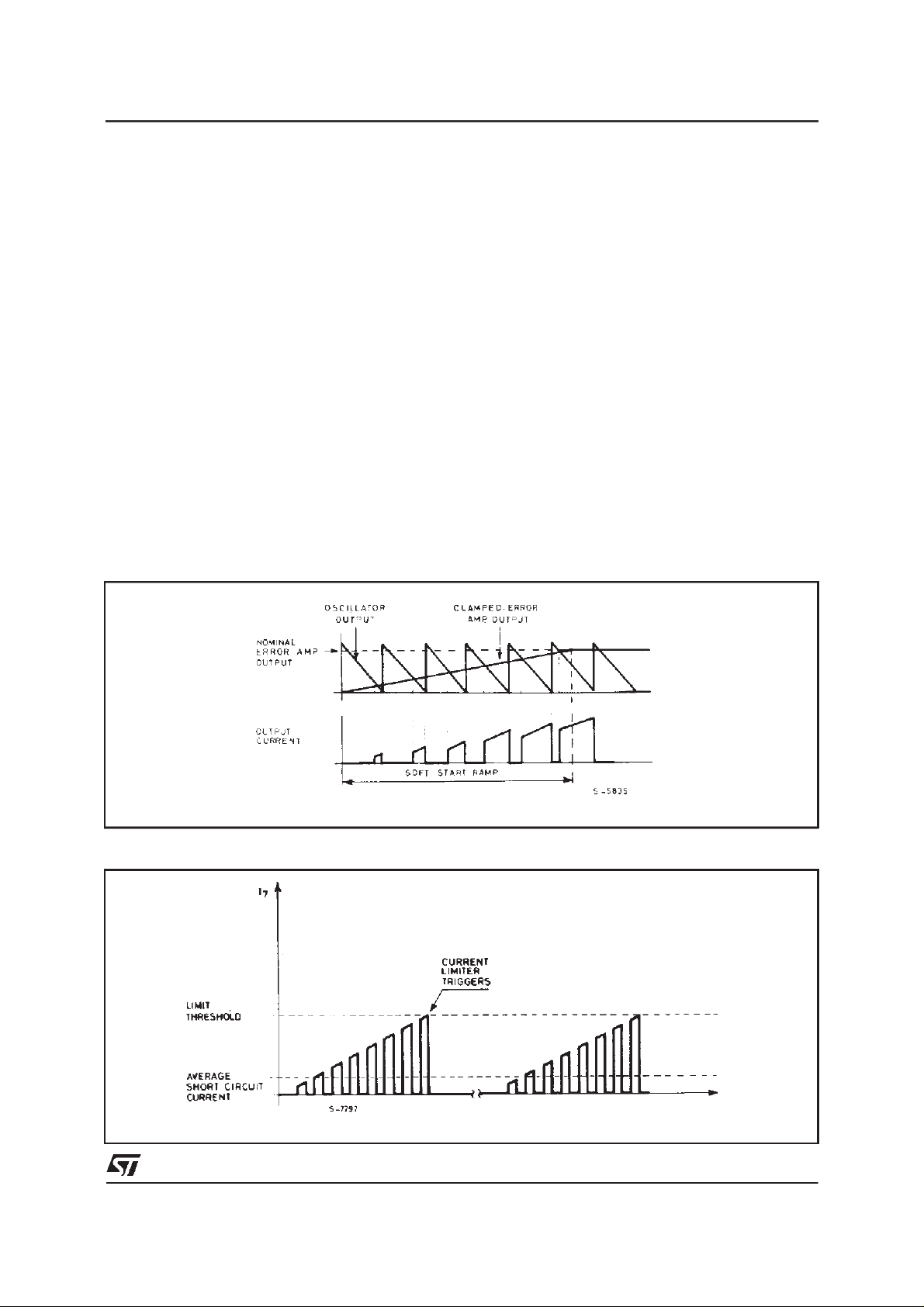
the softstart function.The erroramplifieroutput is
initially clamped by the external capacitor C
and
ss
Figure1. Softstart waveforms
allowedtorise,linearly,asthiscapacitoris charged
by aconstantcurrentsource.Outputoverloadprotection is provided in the form of a current limiter.
The load current is sensed by an internal metal
resistorconnectedtoa comparator.When the load
currentexceedsapresetthresholdthis comparator
sets a flipflop whichdisables the output stage and
dischargesthe soft start capacitor.Asecondcomparator resets the flipflopwhen thevoltageacross
the soft start capacitorhas fallento 0.4V.
The output stage is thusre-enabledandthe output
voltagerisesunder controlof the soft start network.
If the overload condition is still present the limiter
will trigger again when the threshold current is
reached.Theaverageshortcircuitcurrentislimited
to a safevalueby the dead timeintroduced by the
soft start network. The thermaloverload circuit disables circuit operation when the junctiontemperature reaches about 150°C and has hysteresis to
preventunstable conditions.
Figure2. Currentlimiterwaveforms
5/16
Page 6

L4960
Figure3. Testandapplicationcircuit
C6, C7: EKR (ROE)
L1 =150µH at 5A(COGEMA 946042)
CORE TYPE: MAGNETICS 58206-A2MPP
N°TURNS 45, WIRE GAUGE: 0.8mm (20 AWG)
Figure 4. Quiescent drain
currentvs. supplyvoltage (0%
duty cycle)
6/16
Figure 5. Quiescent drain
current vs. supply voltage
(100% duty cycle)
Figure 6. Quiescent drain
current vs. junction temperature(0%duty cycle)
Page 7

L4960
Figure 7. Quiescent drain
current vs. junction temperature (100%duty cycle)
Figure 10. Open loop frequency and phase responde
of error amplifier
Figure 8. Reference voltage
(pin 2) vs. V
i
Figure 11. Switching frequency vs. inputvoltage
Figure 9. Reference voltage
versus junction temperature
(pin 2)
Figure 1 2. Switchi ng frequ en cy vs . j uncti o n tem perature
Figure 13. Switching frequencyvs. R2 (seetestcircuit)
Figure 14. Line transient
response
Figu re 1 5. L oad transi ent
response
7/16
Page 8

L4960
Figure 16. Supply voltage
ripplerejectionvs. frequency
Figure 19. Power dissipation
deratingcurve
Figure 17. Dropout voltage
between pin 1 and pin 7 vs.
currentat pin 7
Figure 2 0. Effici ency vs.
output current
Figure 18 . Dropout voltage
betweenpin1and7vs.
junction temperature
Figure 21. Efficiency vs.
output current
8/16
Figure 22. E ffic iency vs .
output current
Fig ure 2 3. Eff ic ie ncy v s.
output voltage
Page 9

APPLICATION INFORMATION
Figure24. Typicalapplication circuit
L4960
C1,C6,C7: EKR(ROE)
D
: BYW80 OR 5ASCHOTTKY DIODE
1
SUGGESTED INDUCTOR: L
CORE TYPE: MAGNETICS 58206- A2 - MPP
U15/GUP15: N° TURNS: 60, WIRE GAUGE:0.8mm (20 AWG), AIR GAP: 1mm, COGEMA969051.
N°TURNS: 45, WIRE GAUGE: 0.8mm (20 AWG), COGEMA946042
= 150µHat5A
1
Figure25. P.C. board andcomponent layout of
the Fig. 24 (1: 1 scale)
Resistor values for
standard output voltages
V
12V
15V
18V
24V
o
R3 R4
4.7KΩ
4.7KΩ
4.7K
Ω
4.7K
Ω
6.2KΩ
9.1KΩ
12K
18K
Ω
Ω
9/16
Page 10

L4960
APPLICATION INFORMATION
Figure26. A minimal5.1Vfixed regulator;Veryfew component are required
* COGEMA 946042 (TOROID CORE)
** EKR (ROE)
969051 (U15 CORE)
Figure27. Programmablepower supply
Vo= 5.1V to15V
I
= 2.5A max
o
Load regulation (1Ato 2A) = 10mV (V
= 5.1V)
o
10/16
Page 11

L4960
APPLICATION INFORMATION
(continued)
Figure28. Microcomputersupply with + 5.1V,-5V, +12V and -12V outputs
11/16
Page 12

L4960
APPLICATION INFORMATION
(continued)
Figure29. DC-DCconverter5.1V/4A,± 12V/2.5A;a suggestionhowto synchronizeanegativeoutput
L1, L3 = COGEMA 946042 (969051)
L2 = COGEMA946044 (946045)
D
1,D2,D3
= BYW80
Figure30. - InmultiplesuppliesseveralL4960s can be synchronizedas shown
12/16
Page 13

L4960
APPLICATION INFORMATION
(continued)
Figure31. Regulatorfordistributedsupplies
MOUNTINGINSTRUCTION
Thepowerdissipatedinthecircuitmustberemoved
by addingan externalheatsink.
Thanks to the Heptawatt package attaching the
hetsink is very simple, a screw or a compression
spring (clip) beingsufficient. Between the heatsink
Figure32. Mountingexample
andthepackageit isbettertoinserta layerofsilicon
grease, to optimizethe thermal contact,no electrical isolation is neededbetween the two surfaces.
13/16
Page 14

L4960
DIM.
MIN. TYP. MAX. MIN. TYP. MAX.
A 4.8 0.189
C 1.37 0.054
D 2.4 2.8 0.094 0.110
D1 1.2 1.35 0.047 0.053
E 0.35 0.55 0.014 0.022
E1 0.7 0.97 0.028 0.038
F 0.6 0.8 0.024 0.031
F1 0.9 0.035
G 2.34 2.54 2.74 0.095 0.100 0.105
G1 4.88 5.08 5.28 0.193 0.200 0.205
G2 7.42 7.62 7.82 0.295 0.300 0.307
H2 10.4 0.409
H3 10.05 10.4 0.396 0.409
L 16.7 16.9 17.1 0.657 0.668 0.673
L1 14.92
L2 21.24 21.54 21.84 0.386 0.848 0.860
L3 22.27 22.52 22.77 0.877 0.891 0.896
L4 1.29
L5 2.6 2.8 3 0.102 0.110 0.118
L6 15.1 15.5 15.8 0.594 0.610 0.622
L7 6 6.35 6.6 0.236 0.250
L9 0.2 0.008
M 2.55 2.8 3.05 0.100 0.110 0.120
M1 4.83 5.08 5.33 0.190 0.200 0.210
V4 40° (typ.)
Dia 3.65 3.85 0.144 0.152
mm inch
0.587
0.051
0.260
OUTLINE AND
MECHANICAL DATA
Heptawatt V
H3
L
VV
E
L1
M1
A
C
D
M
D1
H2
V4
L9
H1
L5
Dia.
L2
L3
F
E1
E
GG1G2
F
L7
L4
L6
F1H2
HEPTAMEC
14/16
Page 15

L4960
DIM.
MIN. TYP. MAX. MIN. TYP. MAX.
A 4.8 0.189
C 1.37 0.054
D 2.4 2.8 0.094 0.110
D1 1.2 1.35 0.047 0.053
E 0.35 0.55 0.014 0.022
F 0.6 0.8 0.024 0.031
F1 0.9 0.035
G 2.41 2.54 2.67 0.095 0.100 0.105
G1 4.91 5.08 5.21 0.193 0.200 0.205
G2 7.49 7.62 7.8 0.295 0.300 0.307
H2 10.4 0.409
H3 10.05 10.4 0.396 0.409
L 14.2 0.559
L1 4.4
L2 15.8
L3 5.1
L5 2.6 3 0.102 0.118
L6 15.1 15.8 0.594 0.622
L7 6 6.6 0.236
L9 4.44 0.175
Dia 3.65 3.85 0.144 0.152
mm inch
0.173
0.622
0.201
0.260
OUTLINE AND
MECHANICAL DATA
Heptawatt H
15/16
Page 16

L4960
Information furnishedisbelievedto beaccurate andreliable. However, STMicroelectronics assumes no responsibility for the consequences of
use of such information nor for any infringement of patents or other rights of third parties which may result from itsuse.No license is granted
by implicationor otherwise under any patentor patent rights of STMicroelectronics. Specification mentioned in this publication are subject to
change without notice. This publication supersedes and replaces all information previously supplied. STMicroelectronics products are not
authorized for use as criticalcomponentsin lifesupport devices or systems withoutexpress written approval of STMicroelectronics.
The ST logo is a registered trademark of STMicroelectronics
2000 STMicroelectronics – Printed in Italy– All Rights Reserved
STMicroelectronics GROUP OF COMPANIES
Australia - Brazil - China - Finland - France - Germany - HongKong - India- Italy- Japan - Malaysia- Malta- Morocco -
Singapore - Spain - Sweden - Switzerland - United Kingdom- U.S.A.
http://www.st.com
16/16
 Loading...