

Page 1
®
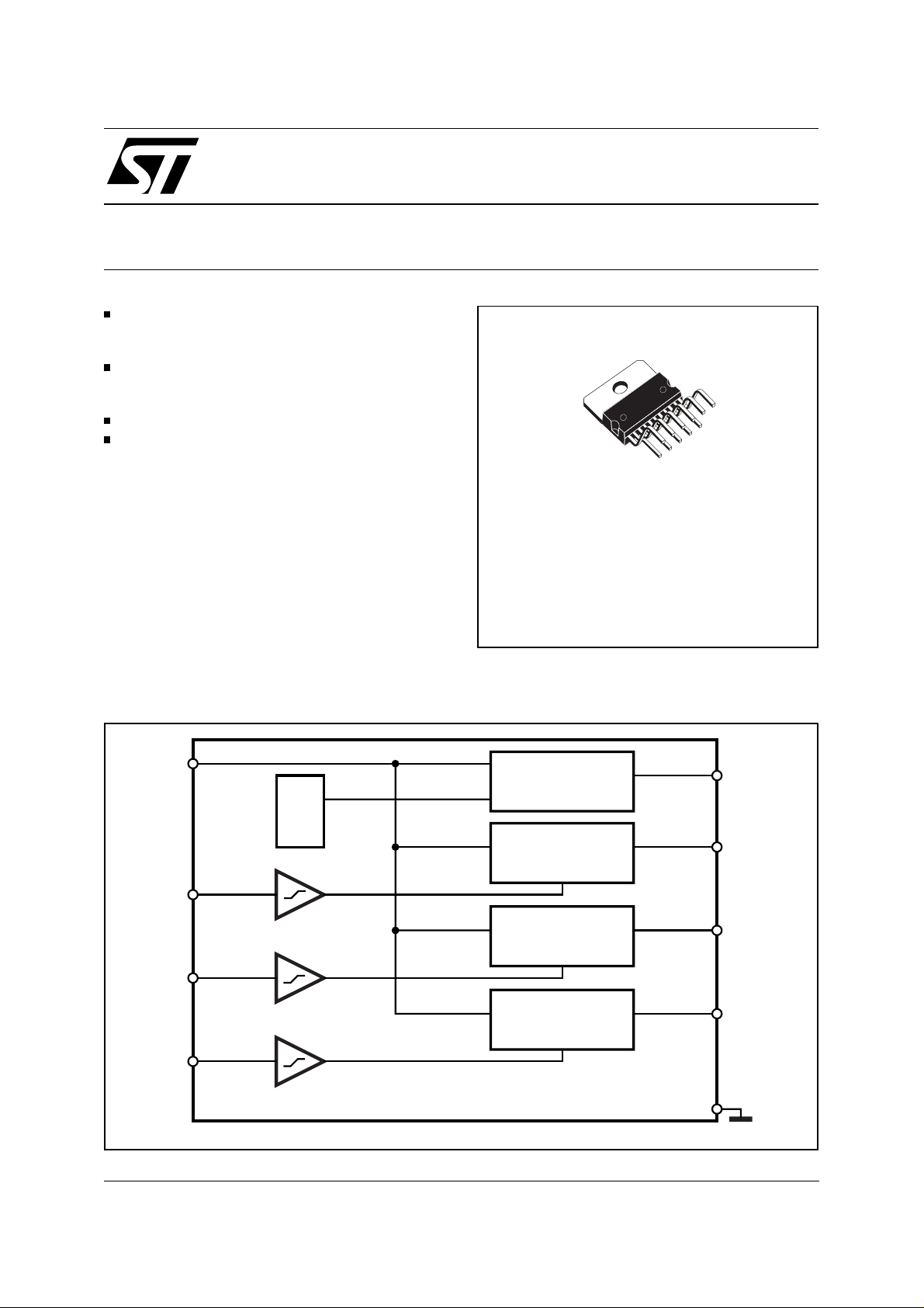
L4959
MULTIFUNCTION VOLTAGE REGULATOR FOR HOME AUDIO
4 OUTPUTS:
12V (1.3A); 12V (0.8A); 8.6V (0.6A); 5.6V
(0.25A) STA N DBY
OUT1 12V(a), OU T2 12V(b) AND OUT3 8.6V
WITH INDEPENDENT ENABLE CONTROL
FOR STAND-BY MODE
SHORT- C IR CUIT P R OT E C TIO N TO GROUND
THERMAL SHUTDOWN
DESCRIPTION
The L4959 is a monolithic Multifunction Voltage
Regulator, designed mainly for supplying Home
Audio systems. The L4959 contains one unswitched linear 5.6V regulator for Micro, two
switched regulators 8.6V and 12V, suitable to
feed CD or CD players and LED, Signal Process.
An additional 12V regulator for Solenoid Motor an
CD_TRAY Driven is also available.
ORDERING NUMBER:
Multiwatt 11
L4959
BLOCK DIAGRAM
2/10
V
S
EN 8V
EN 12V(a)
EN 12V(b)
8
7
5
REF
GEN
D97AU569C
5.6V, 250mA
REGULATOR
8.6V, 600mA
REGULATOR
SWITCHED
12V, 800mA
REGULATOR
SWITCHED
12V, 1.3A
REGULATOR
SWITCHED
3
9
11
1
6
OUT 5.6V
OUT 8.6V
OUT 12V(a)
OUT 12V(b)
GND
January 1999
1/6
Page 2
L4959
ABSOLUTE MAXIMUM RATINGS
Symbol Parameter Value Unit
V
S
I
O
T
op
T
stg
DC Supply Voltage 35 V
Output Current internally limited
Operating Temperature Range 0 to +70 °C
Storage Temperature –40 to 150 °C
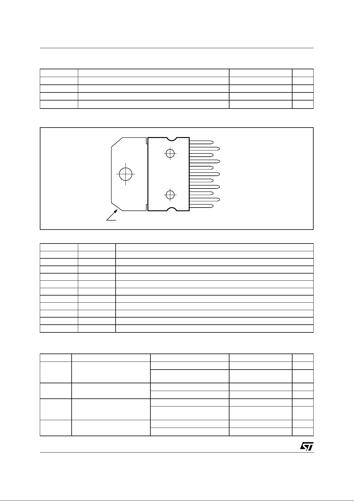
PIN CONNECTION
(Top view)
11
10
9
8
7
6
5
4
3
2
1
TAB CONNECTED TO PIN 6
PIN DESCRIPTION
Pin Pins Description
1 OUT 12V (b) 12V/1.3A SWITCHED OUTPUT VOLTAGE
2V
S
3 OUT 5.6V 5.6V/250mA OUTPUT VOLTAGE
4 N.C. not connected
5 EN 12V (b) Enable 12V/1.3A SWITCHED OUTPUT VOLTAGE
6 GND Ground
7 EN 12V (a) Enable 12V/0.8A SWITCHED OUTPUT VOLTAGE
8 EN 8.6V Enable 8.6V/0.6A SWITCHED OUTPUT VOLTAGE
9 OUT 8.6 8.6V/0.6A SWITCHED OUTPUT VOLTAGE
10 V
S
11 OUT 12V (a) 12V/0.8A SWITCHED OUTPUT VOLTAGE
Supply Voltage
Supply Voltage
D97AU716A
OUT 12V(a)
V
S
OUT 8.6V
EN 8.6V
EN 12V(a)
GND
EN 12V(b)
N.C.
OUT 5.6V
V
S
OUT 12V(b)
QUICK REFERENCE DATA
Symbol Parameter Test Condition Typ. Unit
5V Output Voltage IO = 125mA 5.6 V
14.4V < V
< 21.6V
S
5.6 V
5mA < I < 0.25A
8.6V Output Voltage IO = 300mA 8.6 V
14.4V < V
< 21.6V 5mA < I < 0.6A 8.6 V
S
12V Output Voltage Iout = 400mA 12 V
14.4V < V
< 21.6V
S
12 V
5mA < I < 0.8A
12V Output Voltage Iout = 650mA 12 V
14.4V < VS < 21.6V 5mA < I < 1.3A 12 V
2/6
V
out 5V
V
out 8V
V
out 12Va
V
out 12Vb
Page 3

THERMAL DATA
Symbol Parameter Value Unit
R
th j-case
Thermal Resistance Junction-case 2 °C/W
L4959
ELECTRICAL CHARACTERISTICS
(V
= 18V, T
S
= 25°C, unless otherwise specified.)
case
Symbol Parameter Test Condition Min. Typ. Max. Unit
V
S
Operating Supply Voltage no load 15 22 30 V
loaded (*) 14.4 18 21.6 V
En Output Noise Voltage Any reg. supply,
200 400 µV
f = 100Hz to 20KHz
I
q
Quiescent Current 8 mA
5.6V/250mA OUTPUT VOLTAGE
V
∆V
∆V
V
dropout
out 5V
line
load
I
lim
5V Output Voltage IO = 125mA 5.45 5.9 V
14.4V < V
< 21.6V
S
5.40 6 V
5mA < I < 0.25
Line Regulation 14.4V < VS < 21.6V 5 50 mV
Load Regulation 5mA < Io < 250mA 50 150 mV
Dropout Voltage I
= 250mA 2.05 2.7 V
out
Current Limit VS = 21.6V 250 325 mA
8.6V/0.6A SWITCHED OUTPUT VOLTAGE
V
out 8V
∆V
line
∆V
load
V
dropout
I
lim
SWon Switch ON 2.31 3.5 V
SW off Switch OFF 1.5 2.11 V
SW hyst Switch Hysteresis 200 mV
8.6V Output Voltage IO = 300mA 8.4 9.1 V
14.4V < VS < 21.6V 5mA < I < 0.6A 8.3 9.2 V
Line Regulation 14.4V < VS < 21.6V 5 50 mV
Load Regulation 5mA < Io < 0.6A 50 350 mV
Dropout Voltage I
= 0.6A 2.05 2.7 V
out
Current Limit VS = 21.6V 0.6 0.8 A
12V/0.8A SWITCHED OUTPUT VOLTAGE
V
out12Va
∆V
line
∆V
load
V
dropout
I
lim
SVR Supply Voltage Rejection f = 100Hz
SWon Switch ON 2.31 3.5 V
SW off Switch OFF 1.5 2.11 V
SW hyst Switch Hysteresis 200 mV
12V Output Voltage I
= 400mA 11.7 12.7 V
out
14.4V < VS < 21.6V
11.6 12.8 V
5mA < I < 0.8A
Line Regulation 14.4V < Vs < 21.6V 10 50 mV
Load Regulation 5mA < Io < 0.8A 100 350 mV
Dropout Voltage I
= 0.8A 2.13 2.7 V
out
Current Limit VS = 21.6V 0.8 1.1 A
f = 10KHz
55
40
75 dB
12V/1.3A SWITCHED OUTPUT VOLTAGE
V
out12Vb
∆V
∆V
V
dropout
line
load
I
lim
12V Output Voltage I
= 650mA 11.6 12.6 V
out
14.4V < VS < 21.6V
11.5 12.7 V
5mA < I < 1.3A
Line Regulation 14.4V < Vs < 21.6V 10 50 mV
Load Regulation 5mA < Io < 1.3A 200 450 mV
Dropout Voltage I
= 1.3A 2.15 2.7 V
out
Current Limit VS = 21.6V 1.3 1.7 A
3/6
Page 4

L4959
ELECTRICAL CHARACTERISTICS
(continued)
Symbol Parameter Test Condition Min. Typ. Max. Unit
SVR Supply Voltage Rejection f = 100Hz
f = 10KHz
55
40
75 dB
SWon Switch ON 2.31 3.5 V
SW off Switch OFF 1.5 2.11 V
SW hyst Switch Hysteresis 200 mV
(*) The max value is limited by the power dissipation
Figure 1:
Application and Test Circuit.
+V
S
GND
C1
2200µF
35VL
+5V
C2
0.33µF
V
CC
G
EN8.6V
EN12Va
3
2
10
L4959
6
87 5
EN12Vb
5.6V 0.25A
C3
0.1µF
11
1
9
C4
0.1µF
C5
0.1µF
C6
0.1µF
100µF
16VL
C7
C8
100µF
16VL
C9
100µF
16VL
12Va 0.8A
12Vb 1.3A
8.6V 0.6A
C10
100µF
16VL
µ-PROC
SIGNAL
DECK
CD
Figure 2:
D97AU802
PCB and Components layout of the Figure 1.
4/6
Page 5

L4959
DIM.
MIN. TYP. MAX. MIN. TYP. MAX.
A 5 0.197
B 2.65 0.104
C 1.6 0.063
D 1 0.039
E 0.49 0.55 0 .019 0.022
F 0.88 0.95 0.035 0.037
G 1.45 1.7 1.95 0 .057 0.067 0.077
G1 16.75 17 17.25 0.659 0.669 0.679
H1 19.6 0.772
H2 20.2 0.795
L 21.9 22.2 22.5 0.862 0.874 0.886
L1 21.7 22.1 22.5 0.854 0.87 0.886
L2 17.4 18.1 0.685 0.713
L3 17.25 17.5 17.75 0.679 0.689 0.699
L4 10.3 10.7 10.9 0.406 0.421 0.429
L7 2.65 2.9 0.104 0.114
M 4.25 4.55 4.85 0.167 0.179 0.191
M1 4.73 5.08 5.43 0.186 0.200 0.214
S 1.9 2.6 0.075 0.102
S1 1.9 2.6 0.075 0.102
Dia1 3.65 3.85 0.144 0.152
mm inch
OUTLINE AND
MECHANICAL DATA
Multiwatt11 V
5/6
Page 6

L4959
Information furnishe d is beli eved to be accu rate and reliable. However, STMicroelec tronics assumes no res ponsibility for the consequences
of use of such i nformation nor for any i nfringement of patents or ot her rights of third par ties which may result from its use. No license i s
granted by impli cation or otherwis e under any patent or patent righ ts of STMicroelect ronics. Specifica tion mentioned in this publication are
subject to change without notic e. This public ation supers edes and replaces all information prev iously supplied. STMic roelec tronic s products
are not authorized for use as critical components in life support devices or systems without express written approval of STMicroelectronics.
The ST logo is a registered trademark of STMicroelect roni cs
© 1999 STMicroelectronics – Printed in Italy – All Rights Reserved
STMicroelectronics GROUP OF COMPANIES
Australia - Brazil - Canada - China - France - Germany - Italy - Japan - Korea - Malaysia - Malta - Mexico - Morocco - The Nether la nds -
Singapore - Spain - Sweden - Switzerland - Taiwan - Thailand - United Kingdom - U.S.A.
http://www.st.com
6/6
 Loading...