

Page 1
Order this document from L4949/D
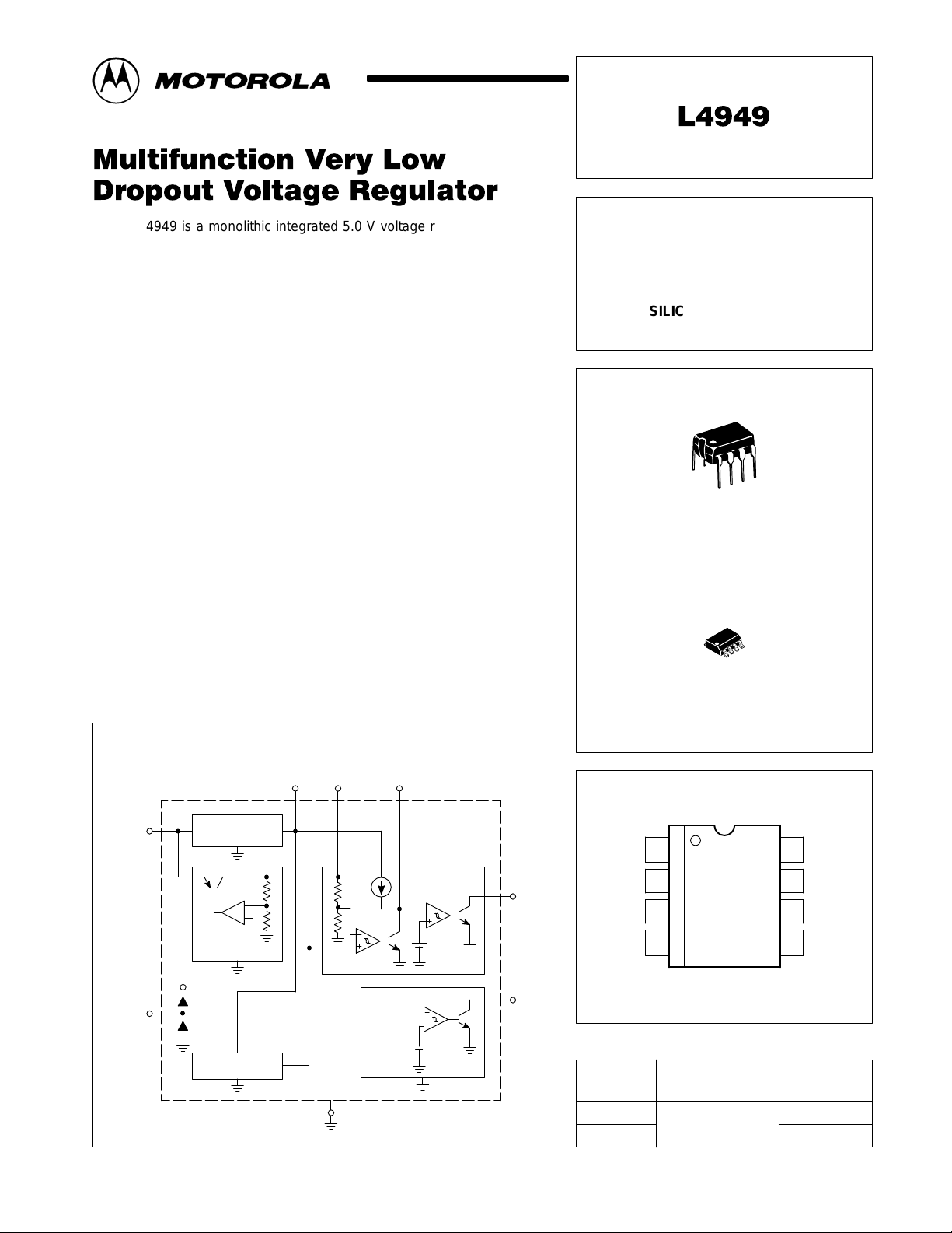
The L4949 is a monolithic integrated 5.0 V voltage regulator with a very
low dropout and additional functions such as power–on reset and input
voltage sense.
It is designed for supplying the micro–computer controlled systems
especially in automotive applications.
• Operating DC Supply Voltage Range 5.0 V to 28 V
• Transient Supply Voltage Up to 40 V
• Extremely Low Quiescent Current in Standby Mode
• High Precision Standby Output Voltage 5.0 V ±1%
• Output Current Capability Up to 100 mA
• Very Low Dropout Voltage Less Than 0.4 V
• Reset Circuit Sensing The Output Voltage
• Programmable Reset Pulse Delay With External Capacitor
• Voltage Sense Comparator
• Thermal Shutdown and Short Circuit Protections
MULTIFUNCTION
VERY LOW DROPOUT
VOLTAGE REGULATOR
SILICON MONOLITHIC
INTEGRATED CIRCUIT
8
1
N SUFFIX
PLASTIC PACKAGE
CASE 626
8
1
Supply
Voltage (VCC)
Sense
Input
(Si)
1
V
s
2
Representative Block Diagram
Output
Preregulator
6.0 V
Regulator
1.23 V
Voltage (V
V
38 4
Z
ref
out
2.0
Reset
Gnd
5
)
µ
A
C
T
Sense
+
2.0 V
–
+
1.23 V
–
Reset
6
Sense
Output
(So)
7
D SUFFIX
PLASTIC PACKAGE
CASE 751
PIN CONNECTIONS
V
1
CC
S
2
i
V
3
Z
C
4
T
(Top View)
8
7
6
5
V
out
S
o
Reset
Gnd
ORDERING INFORMATION
Operating
Device
L4949N
L4949D
Motorola, Inc. 1998 Rev 1
Temperature Range
TJ = –40° to +125°C
Package
DIP–8
SO–8
Page 2
ABSOLUTE MAXIMUM RATINGS
ÁÁÁ
ÁÁÁ
ÁÁÁ
ÁÁÁ
ÁÁÁ
ÁÁÁ
ÁÁÁ
ÁÁÁ
ÁÁÁ
ÁÁÁ
ÁÁÁ
ÁÁÁ
ÁÁÁ
which damage to the device may occur.)
Rating
DC Operating Supply Voltage
Transient Supply Voltage (t < 1.0 s)
Output Current
Output Voltage
Sense Input Current
Sense Input Voltage
Output Voltages
Reset Output
Sense Output
Output Currents
Reset Output
Sense Output
Preregulator Output Voltage
Preregulator Output Current
ESD Protection at any pin
Human Body Model
Machine Model
Thermal Resistance, Junction–to–Air
P Suffix, DIP–8 Plastic Package, Case 626
D Suffix, SO–8 Plastic Package, Case 751
Maximim Junction Temperature
Storage Temperature Range
NOTE: ESD data available upon request.
L4949
(Absolute Maximum Ratings indicate limits beyond
Symbol Value Unit
V
VCC
I
out
V
I
V
V
Reset
V
I
Reset
I
SO
V
R
θJA
T
T
CC
out
SI
SI
SO
Z
I
Z
–
–
J
stg
TR
28
40
Internally
Limited
20
±1.0
V
CC
20
20
5.0
5.0
7.0
5.0
2000
400
100
200
150
–65 to +150
mA
mA
mA
°C/W
V
V
–
V
–
V
V
V
°C
°C
ELECTRICAL CHARACTERISTICS (V
= 14 V, –40°C < TJ < 125°C, unless otherwise specified.)
CC
Characteristic
Output Voltage (TJ = 25°C, I
Output Voltage (6.0 V < VCC < 28 V, 1.0 mA < I
Output Voltage (VCC = 35 V, t < 1.0 s, 1.0 mA < I
= 1.0 mA)
out
< 50 mA)
out
out
< 50 mA)
Dropout Voltage
I
= 10 mA
out
I
= 50 mA
out
I
= 100 mA
out
Input to Output Voltage Difference in Undervoltage Condition
(VCC = 4.0 V, I
Line Regulation (6.0 V < VCC < 28 V, I
Load Regulation (1.0 mA < I
= 35 mA)
out
< 100 mA)
out
= 1.0 mA)
out
Current Limit
V
= 4.5 V
out
V
= 0 V
out
Quiescent Current (I
БББББББББББББББББ
Quiescent Current (I
БББББББББББББББББ
= 0.3 mA, TJ < 100°C)
out
= 100 mA)
out
Symbol Min Typ Max Unit
V
out
V
out
V
out
V
drop
V
IO
Reg
line
Reg
load
I
Lim
I
QSE
ÁÁÁ
I
Q
ÁÁÁ
4.95
4.9
4.9
–
–
–
–
–
–
105
–
ÁÁ–ÁÁ
ÁÁ–ÁÁ–ÁÁ
5.0
5.0
5.0
0.1
0.2
0.3
0.2
1.0
8.0
200
100
150
5.05
5.1
5.1
0.25
0.40
0.50
0.4
20
30
400
–
260
ÁÁ
5.0
ÁÁ
ÁÁ
V
V
V
V
V
mV
mV
mA
µA
mA
2
MOTOROLA ANALOG IC DEVICE DATA
Page 3

L4949
ÁÁÁ
ÁÁÁ
ÁÁÁ
ÁÁÁ
ÁÁÁ
ÁÁÁ
ÁÁÁ
ÁÁÁ
ÁÁÁ
ÁÁÁ
ÁÁÁ
ÁÁÁ
ÁÁÁ
ÁÁÁ
ÁÁÁ
ÁÁÁ
ELECTRICAL CHARACTERISTICS (continued) (V
= 14 V, –40°C < TJ < 125°C, unless otherwise specified.)
CC
Characteristic UnitMaxTypMinSymbol
RESET
Reset Threshold Voltage
Reset Threshold Hysteresis
@ TJ = 25°C
@ TJ = –40 to +125°C
Reset Pulse Delay (CT = 100 nF, tR ≥ 100 µs)
БББББББББББББББББ
Reset Reaction Time (CT = 100 nF)
БББББББББББББББББ
Reset Output Low Voltage (R
БББББББББББББББББ
Reset Output High Leakage Current (V
БББББББББББББББББ
Delay Comparator Threshold
БББББББББББББББББ
Delay Comparator Threshold Hysteresis
БББББББББББББББББ
Reset
= 10 kΩ to V
= 5.0 V)
Reset
, VCC ≥ 3.0 V)
out
SENSE
Sense Low Threshold (VSI Decreasing = 1.5 V to 1.0 V)
Sense Threshold Hysteresis
Sense Output Low Voltage
(VSI ≤ 1.16 V , VCC ≥ 3.0 V, RSO = 10 kΩ to V
out
)
Sense Output Leakage (VSO = 5.0 V, VSI ≥ 1.5 V)
Sense Input Current
PREREGULAT OR
Preregulator Output Voltage (IZ = 10 µA)
V
Resth
V
Resth,hys
t
ResD
ÁÁÁ
t
ResR
ÁÁÁ
V
ResL
ÁÁÁ
I
ResH
ÁÁÁ
V
CTth
ÁÁÁ
V
CTth, hys
ÁÁÁ
V
SOth
V
SOth,hys
V
SOL
I
SOH
I
SI
V
Z
–
V
– 0.5
out
50
50
ÁÁ55ÁÁ
ÁÁ–ÁÁ
ÁÁ–ÁÁ–ÁÁ
ÁÁ–ÁÁ–ÁÁ
ÁÁ–ÁÁ
ÁÁ–ÁÁ
1.16
20
–
–
–1.0
–
100
–
100
5.0
2.0
100
1.23
100
–
–
0.1
6.3
–
200
300
180
ÁÁ
30
ÁÁ
0.4
1.0
–
ÁÁ
–
ÁÁ
1.35
200
0.4
1.0
1.0
–
V
mV
ms
ÁÁ
µs
ÁÁ
V
ÁÁ
µA
ÁÁ
V
ÁÁ
mV
ÁÁ
V
mV
V
µA
µA
V
Pin
ÁÁ
1
2
3
4
5
6
7
8
5.04
5.02
5.0
, OUTPUT VOL TAGE (V)
4.98
out
V
Symbol
ÁÁÁÁ
V
CC
S
i
V
Z
C
T
Gnd
Reset
S
O
V
out
ББББББББББББББББББББББББ
Supply Voltage
Input of Sense Comparator
Output of Preregulator
Reset Delay Capacitor
Ground
Output of Reset Comparator
Output of Sense Comparator
Main Regulator Output
TYPICAL CHARACTERIZA TION CUR VES
Figure 1. Output Voltage versus
Junction T emperature
VCC = 14 V
I
= 1.0 mA
out
PIN FUNCTION DESCRIPTION
Description
6.0
5.0
4.0
3.0
2.0
, OUTPUT VOL TAGE (V)
out
V
1.0
Figure 2. Output Voltage versus
Supply V oltage
TJ = 25°C
RL = 5.0 k
RL = 100
Ω
4.96
–40 –20 0 40 6020 100 120
TJ, JUNCTION TEMPERATURE (
80
°
C)
MOTOROLA ANALOG IC DEVICE DATA
0
010
1.0
2.0 3.0 4.0 5.0 6.0 7.0 8.0 9.0
V
, SUPPLY VOLT AGE (V)
CC
3
Page 4

L4949
TYPICAL CHARACTERIZA TION CUR VES (continued)
Figure 3. Dropout Voltage versus
Output Current
250
TJ = 25°C
200
150
100
, DROPOUT VOLTAGE (mV)
50
drop
V
0
0.1 100
I
, OUTPUT CURRENT (mA)
out
101.0
Figure 5. Quiescent Current versus
Output Current
3.0
VCC = 14 V
2.5
TJ = 25
°
C
Figure 4. Dropout Voltage versus
Junction T emperature
0.40
I
= 100 mA
0.30
0.20
, DROPOUT VOLTAGE (mV)
0.10
drop
V
0
–40 –20 0 40 6020 100 120
TJ, JUNCTION TEMPERATURE (
out
I
out
I
out
= 50 mA
= 10 mA
80
°
C)
Figure 6. Quiescent Current versus
Supply V oltage
3.0
2.5
TJ = 25°C
2.0
1.5
1.0
, QUIESCENT CURRENT (mA)
Q
0.5
I
0
0.1 1.0 10 100
I
, OUTPUT CURRENT (mA)
out
Figure 7. Reset Output versus
Regulator Output Voltage
6.0
TJ = 25°C
5.0
Resistor 10 k
from Reset Output
4.0
to 5.0 V
3.0
, RESET OUTPUT (V)
2.0
Reset
V
1.0
0
4.0 4.1
4.2 4.3 4.4 4.5 4.6 4.7 4.8 4.9 5.0
V
, OUTPUT VOLTAGE (V)
out
2.0
RL = 100
1.5
1.0
, QUIESCENT CURRENT (mA)
Q
0.5
I
0
0 5.0 10 15 20 25 30
VCC, SUPPLY VOLT AGE (V)
Ω
RL = 5.0 k
Figure 8. Reset Thresholds versus
Junction T emperature
4.7
4.66
4.62
4.58
4.54
4.5
, RESET THRESHOLD VOLTAGE (V)
4.46
Reset
V
4.42
Upper Threshold
Lower Threshold
–40 –20
0 20 40 60 80 100 120
TJ, JUNCTION TEMPERATURE (
°
C)
4
MOTOROLA ANALOG IC DEVICE DATA
Page 5

L4949
TYPICAL CHARACTERIZA TION CUR VES (continued)
Figure 9. Sense Output versus
Sense Input V oltage
6.0
TJ = 25°C
5.0
4.0
Resistor 10 k
from Sense Output
to 5.0 V
3.0
2.0
, SENSE OUTPUT VOL TAGE (V)
1.0
SO
V
0
1.0 1.15
1.11.05
1.2 1.25 1.3 1.35 1.4 1.45 1.5
VSI, SENSE INPUT VOLTAGE (V)
APPLICATION INFORMATION
Supply V oltage Transient
High supply voltage transients can cause a reset output
signal perturbation. For supply voltages greater than 8.0 V
the circuit shows a high immunity of the reset output against
supply transients of more than 100 V/µs. For supply voltages
Figure 10. Sense Thresholds versus
Junction T emperature
1.4
1.38
1.36
1.34
1.32
1.3
1.28
, SENSE INPUT VOLTAGE (V)
1.24
SI
V
1.22
1.2
Upper Threshold
Lower Threshold1.26
–40 –20
0 20 40 60 80 100 120
°
TJ, JUNCTION TEMPERATURE (
C)
less than 8.0 V supply transients of more than 0.4 V/µs can
cause a reset signal perturbation. To improve the transient
behavior for supply voltages less than 8.0 V a capacitor at Pin
3 can be used. A capacitor at Pin 3 (C3 ≤ 1.0 µF) reduces
also the output noise.
Figure 11. Application Schematic
V
out
Reset
C
2.0
O
C
T
µ
A
Sense
+
–
+
–
6
2.0 V
RSO10 k
7
1.23 V
10 k
Ω
V
Ω
Reset
out
S
o
C3
V
Z
(optional)
V
bat
V
CC
1
C
s
S
i
2
Preregulator
Regulator
V
CC
1.23 V
6.0 V
ref
38 4
NOTES: 1. For stability: Cs ≥ 1.0 µF, CO ≥ 4.7 µF, ESR < 10 Ω at 10 kHz
2. Recommended for application: Cs = CO = 10 µF
MOTOROLA ANALOG IC DEVICE DATA
5
Gnd
5
Page 6

L4949
OPERA TING DESCRIPTION
The L4949 is a monolithic integrated low dropout voltage
regulator. Several outstanding features and auxiliary
functions are implemented to meet the requirements of
supplying microprocessor systems in automotive
applications. Nevertheless, it is suitable also in other
applications where the present functions are required. The
modular approach of this device allows the use of other
features and functions independently when required.
V oltage Regulator
The voltage regulator uses an isolated Collector Vertical
PNP transistor as a regulating element. With this structure,
very low dropout voltage at currents up to 100 mA is
obtained. The dropout operation of the standby regulator is
maintained down to 3.0 V input supply voltage. The output
voltage is regulated up to the transient input supply voltage of
35 V. With this feature no functional interruption due to
overvoltage pulses is generated.
The typical curve showing the standby output voltage as a
function of the input supply voltage is shown in Figure 13.
The current consumption of the device (quiescent current)
is less than 200 µA.
To reduce the quiescent current peak in the undervoltage
region and to improve the transient response in this region,
the dropout voltage is controlled. The quiescent current as a
function of the supply input voltage is shown in Figure 14.
Short Circuit Protection:
The maximum output current is internally limited. In case
of short circuit, the output current is foldback current limited
as described in Figure 12.
Figure 13. Output V oltage versus Supply Voltage
V
out
V
5.0 V
out
V
CC
Figure 14. Quiescent Current versus Supply V oltage
3.0
2.5
2.0
1.5
1.0
, QUIESCENT CURRENT (mA)
Q
0.5
I
TJ = 25°C
RL = 100
RL = 5.0 k
Ω
35 V5.0 V2.0 V0 V
Figure 12. Foldback Characteristic of V
10
(V)
5.0
out
V
0
20 100 200
I
(mA)
out
out
0
0 5.0 10 15 20 25 30
VCC, SUPPLY VOLT AGE (V)
Preregulator
T o improve the transient immunity a preregulator stabilizes
the internal supply voltage to 6.0 V. This internal voltage is
present at Pin 3 (VZ). This voltage should not be used as an
output because the output capability is very small (≤ 100 µA).
This output may be used as an option when better
transient behavior for supply voltages less than 8.0 V is
required. In this case a capacitor (100 nF – 1.0 µF) must be
connected between Pin 3 and Gnd. If this feature is not used
Pin 3 must be left open.
6
MOTOROLA ANALOG IC DEVICE DATA
Page 7

Reset Circuit
The block circuit diagram of the reset circuit is shown in
Figure 15.
The reset circuit supervises the output voltage. The reset
thereshold of 4.5 V is defined with the internal reference
voltage and standby output drivider.
The reset pulse delay time tRD, is defined with the charge
time of an external capacitor CT:
CTx2.0V
tRD+
2.0mA
The reaction time of the reset circuit originates from the
discharge time limitation of the reset capacitor CT and is
proportional to the value of CT. The reaction time of the reset
circuit increases the noise immunity .
Figure 15. Reset Circuit
1.23 V V
ref
2.0
µ
Out
Reg
22 k
A
C
T
+
2.0 V
–
Reset
L4949
Standby output voltage drops below the reset threshold
only a bit longer than the reaction time results in a shorter
reset delay time.
The nominal reset delay time will be generated for standby
output voltage drops longer than approximately 50 µs. The
typical reset output waveforms are shown in Figure 16.
Figure 16. T ypical Reset Output Waveforms
t
RD
40 V
t
R
Output
Overload
V
out
5.0 V
VRT + 0.1 V
UKT
3.0 V
Reset
V
in
V
out1
t
RD
t
RR
Switch On Input Drop Dump
Sense Comparator
The sense comparator compares an input signal with an
internal voltage reference of typical 1.23 V. The use of an
external voltage divider makes this comparator very flexible
in the application.
It can be used to supervise the input voltage either before
or after the protection diode and to give additional information
to the microprocessor like low voltage warnings.
t
Switch Off
MOTOROLA ANALOG IC DEVICE DATA
7
Page 8

NOTE 2
–T–
SEATING
PLANE
H
A
E
B
C
A1
58
–B–
14
F
–A–
C
N
D
G
0.13 (0.005) B
M
D
58
0.25MB
1
H
4
e
A
B
SS
A0.25MCB
L4949
OUTLINE DIMENSIONS
N SUFFIX
PLASTIC PACKAGE
CASE 626–05
ISSUE K
L
J
K
T
SEATING
PLANE
0.10
A
M
M
M
D SUFFIX
PLASTIC PACKAGE
CASE 751–05
ISSUE S
M
h
X 45
_
q
STYLE 1:
PIN 1. AC IN
2. DC + IN
3. DC – IN
4. AC IN
5. GROUND
6. OUTPUT
7. AUXILIARY
8. V
C
L
CC
NOTES:
1. DIMENSION L TO CENTER OF LEAD WHEN
FORMED PARALLEL.
2. PACKAGE CONTOUR OPTIONAL (ROUND OR
SQUARE CORNERS).
3. DIMENSIONING AND TOLERANCING PER ANSI
Y14.5M, 1982.
DIM MIN MAX MIN MAX
A 9.40 10.16 0.370 0.400
B 6.10 6.60 0.240 0.260
C 3.94 4.45 0.155 0.175
D 0.38 0.51 0.015 0.020
F 1.02 1.78 0.040 0.070
G 2.54 BSC 0.100 BSC
H 0.76 1.27 0.030 0.050
J 0.20 0.30 0.008 0.012
K 2.92 3.43 0.115 0.135
L 7.62 BSC 0.300 BSC
M ––– 10 ––– 10
N 0.76 1.01 0.030 0.040
NOTES:
1. DIMENSIONING AND TOLERANCING PER ASME
Y14.5M, 1994.
2. DIMENSIONS ARE IN MILLIMETERS.
3. DIMENSION D AND E DO NOT INCLUDE MOLD
PROTRUSION.
4. MAXIMUM MOLD PROTRUSION 0.15 PER SIDE.
5. DIMENSION B DOES NOT INCLUDE MOLD
PROTRUSION. ALLOWABLE DAMBAR
PROTRUSION SHALL BE 0.127 TOTAL IN EXCESS
OF THE B DIMENSION AT MAXIMUM MATERIAL
CONDITION.
MILLIMETERS
DIM MIN MAX
A 1.35 1.75
A1 0.10 0.25
B 0.35 0.49
C 0.18 0.25
D 4.80 5.00
E
3.80 4.00
1.27 BSCe
H 5.80 6.20
h
0.25 0.50
L 0.40 1.25
0 7
q
INCHESMILLIMETERS
__
__
Motorola reserves the right to make changes without further notice to any products herein. Motorola makes no warranty , representation or guarantee regarding
the suitability of its products for any particular purpose, nor does Motorola assume any liability arising out of the application or use of any product or circuit, and
specifically disclaims any and all liability, including without limitation consequential or incidental damages. “T ypical” parameters which may be provided in Motorola
data sheets and/or specifications can and do vary in different applications and actual performance may vary over time. All operating parameters, including “Typicals”
must be validated for each customer application by customer’s technical experts. Motorola does not convey any license under its patent rights nor the rights of
others. Motorola products are not designed, intended, or authorized for use as components in systems intended for surgical implant into the body, or other
applications intended to support or sustain life, or for any other application in which the failure of the Motorola product could create a situation where personal injury
or death may occur. Should Buyer purchase or use Motorola products for any such unintended or unauthorized application, Buyer shall indemnify and hold Motorola
and its officers, employees, subsidiaries, affiliates, and distributors harmless against all claims, costs, damages, and expenses, and reasonable attorney fees
arising out of, directly or indirectly, any claim of personal injury or death associated with such unintended or unauthorized use, even if such claim alleges that
Motorola was negligent regarding the design or manufacture of the part. Motorola and are registered trademarks of Motorola, Inc. Motorola, Inc. is an Equal
Opportunity/Affirmative Action Employer.
Mfax is a trademark of Motorola, Inc.
How to reach us:
USA/EUROPE/Locations Not Listed: Motorola Literature Distribution; JAPAN: Motorola Japan Ltd.; SPD, Strategic Planning Office, 141,
P.O. Box 5405, Denver, Colorado 80217. 1–303–675–2140 or 1–800–441–2447 4–32–1 Nishi–Gotanda, Shinagawa–ku, Tokyo, Japan. 81–3–5487–8488
Customer Focus Center: 1–800–521–6274
Mfax: RMFAX0@email.sps.mot.com – TOUCHTONE 1–602–244–6609 ASIA/PACIFIC: Motorola Semiconductors H.K. Ltd.; 8B Tai Ping Industrial Park,
Moto rola Fax Back Syste m – US & Canada ONLY 1–800–774–1848 51 Ting Kok Road, T ai Po, N.T., Hong Kong. 852–26629298
– http://sps.motorola.com/mfax/
HOME PAGE: http://motorola.com/sps/
8
◊
MOTOROLA ANALOG IC DEVICE DATA
L4949/D
 Loading...