

Page 1
L4948
QUAD VOLTAGE REGULATOR WITH INHIBIT AND RESET
4 OUTPUTS: 10V (300mA); 8V (400mA); 5V
(600mA);5V (100mA)
ALL FOUR OUTPUTS ARE LOW DROP
5V (100mA) ST-BY OUTPUT VOLTAGE
EARLY WARNING OUTPUT FOR SUPPLY
UNDERVOLTAGE(LVW)
THERMAL SHUTDOWN AND CURRENT
LIMITATION(FOLDBACK)
REVERSE BATTERY AND LOAD DUMP
PROTECTION
INHIBIT (ON/OFF)AND RESET FUNCTIONS
DESCRIPTION
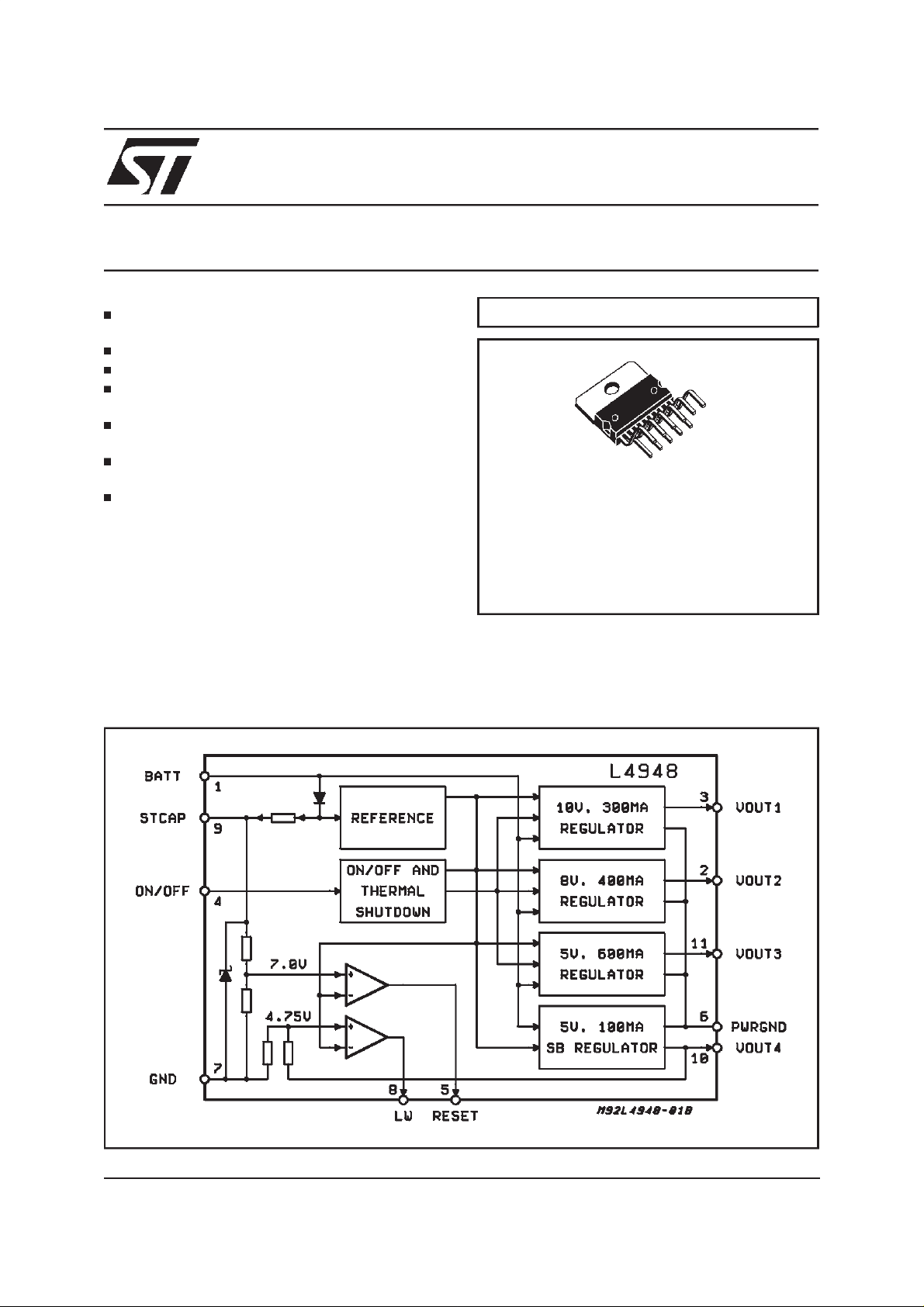
The L4948 is a quad output low drop voltage
regulator. All four outputs are low drop: 10V at
300mA (V
) and a 5V st-by line at 100mA (VO4).
(V
O3
The IC includes a monitoring circuit to warn if a
low voltage or no voltage condition is occurring.
V
O1,2,3
The STCAP pin allows the battery voltage to de-
BLOCK DIAGRAM
), 8V at 400mA (VO2), 5V at 600mA
O1
are offduring st-by mode.
MULTIPOWER BCD TECHNOLOGY
Multiwatt 11
ORDERING NUMBER: L4948
cay slowly giving theµP time to store data. This
IC is designed for supplying microcomputer controlled systems specially in automotive applications.
June 2000
1/9
Page 2
L4948
OPERATINGCONDITION
Symbol Parameter Value Unit
V
S
I
L
ABSOLUTE MAXIMUM RATINGS
Symbol Parameter Value Unit
V
S
V
I
V
O
T
stg
T
j
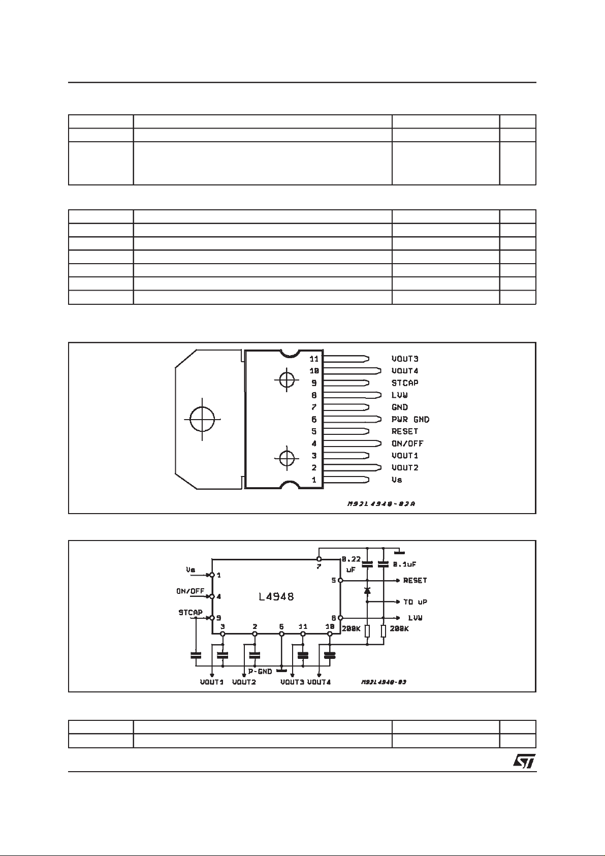
PIN CONNECTION
Supply Voltage -15 to 27 V
Load Current I
O1
I
O2
I
O3
I
O4
300
400
600
100
Supply Voltage -35 to 60 V
Input Voltage (ON/OFF) 0 to 12 V
Output Voltage (LVW, Reset) 0 to 12 V
Storage Temperature Range -65 to 150
Junction Temperature Range max 150
Load Dump (5ms rise, 115ms decay) 60 V
mA
mA
mA
mA
C
°
C
°
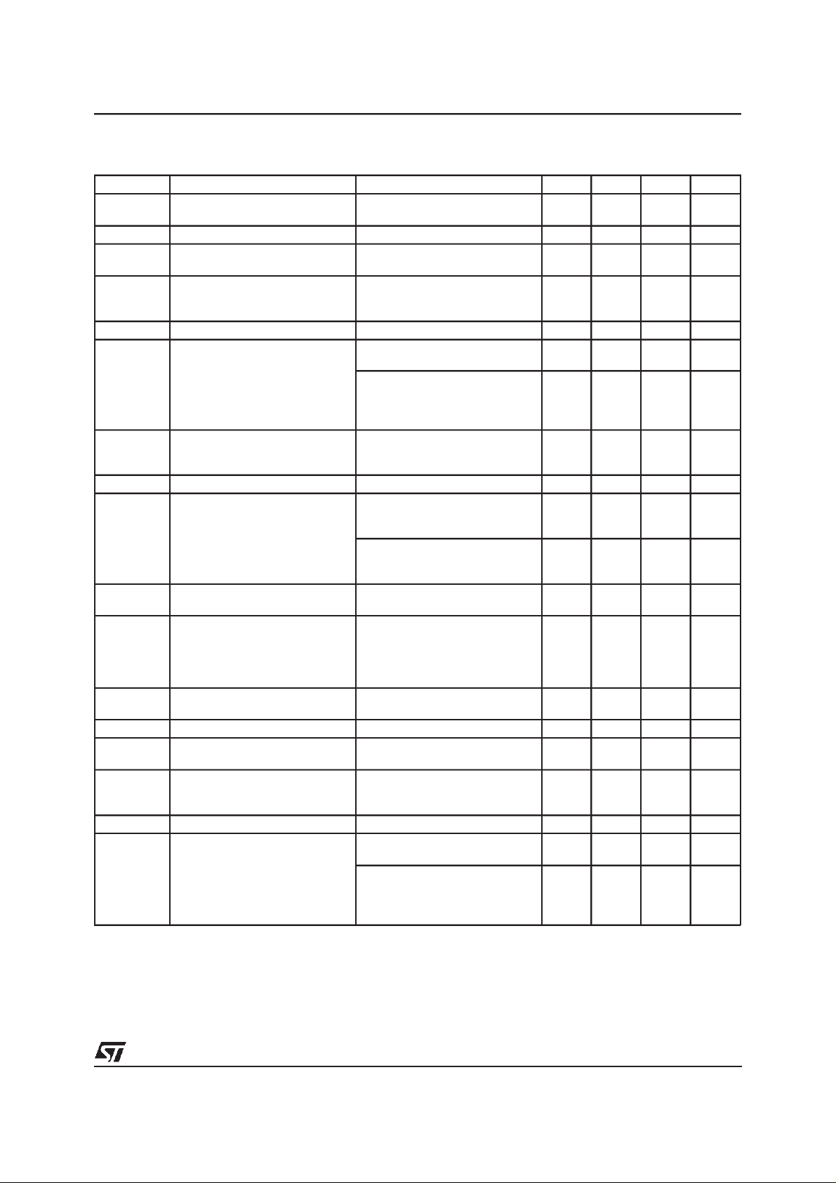
APPLICATIONCIRCUIT
THERMAL DATA
Symbol Parameter Value Unit
Thermal Resistance Junction-case max 2 °C/W
2/9
R
th j-case
Page 3
L4948
ELECTRICAL CHARACTERISTICS (VS= 10.5 to 16V; IO1= 6mA, IO2= 8mA, IO3= 4mA; IO4= 0.4mA;
C
=10µF max; T
O
Symbol Parameter Test Condition Min. Typ. Max. Unit
V
∆
V
S-VO1
V
V
V
O1
V
O1
I
Q
Ι
L
O1
O1
O1
Output Voltage IO1= 300mA; T
Load Regulation IO1= 6 to 300mA 150 mV
Quiescent Current (∆IS)V
Dropout Voltage IO1 = 300mA
Current Limit (Foldback) note1 VO1= 0V 360 800 mA
Max Bat.Trans. RO = 100Ω
Rev. Voltage Trans. VS= -35V; t≤1ms; RO= 100
Rev. Voltage . VS= -15V; RO = 100Ω -0.4 1 V
Ripple rejection f
∆V
O1
Line Regulation
∆V
Output Noise Check Output for AC noise
V
∆V
V
S-VO2
V
O2
O2
∆I
Q
Ι
L
O2
Output Voltage IO2= 400mA; T
Load Regulation IO2 = 8 to 400mA 150 mV
Quiescent Current (∆IS)VS= 14V; IO2= 8mA;
Dropout Voltage IO2= 400mA
Current Limit (Foldback) note1 VO2= 0V 480 960 mA
Max Bat.Trans. RO= 100Ω
= -40to 85°C, unlessotherwisespecified.)
amb
11V < V
S
V
S
RampV
Hold V
RampV
T
amb
< 16V all temps
S
= 14V; IO1= 6mA;
=14V ; IO1= 300mA;
from14 to60V in3-5ms 11 V
S
at 60V for 10ms
S
from60 to14V in3-5ms;
S
=25°C;
all temps
amb
=25°C;
T
=25°C;
amb
all temps
9.7
9.5
9.7
9.5
10
10
10
10
10.3
10.5
10
30
400
600
2
10.3
10.5
Ω
CheckV
I
O1,Tamb
=1KHz;1VppAC;VS=14V
O
= 180mA; IO2= 200mA
O1
=25°C;
all temps
;
9.7
9.5
50
10
10
10.3
10.5
IO3= 400mA; IO4= 40mA;
f
O=10KHz;1VppAC;V
I
= 180mA; IO2= 200mA
O1
=14V
S
;
50 dB
IO3= 400mA; IO4= 40mA;
across VSrange VS= 11V to 26V 50 mV
O1
400
using a 100KHz LP filter
Check Output for AC noise
200
using an A weighted filter (2020KHz)
=25°C;
amb
all temps
7.75
7.60
8
8.25
8
8.40
10
V
= 14V; IO2= 400mA;
S
set V
set V
RampV
Hold V
RampV
T
amb
+1V; T
S=VO2
+1.5V;all temps
S=VO2
from14 to60V in3-5ms 9 V
S
at 60V for 10ms
S
from60 to14V in3-5ms;
S
=25°C;
all temps
amb
=25°C;
7.75
7.60
8
8
35
400
600
2
8.25
8.40
V
V
mA
mA
mV
mV
V
V
V
V
V
dB
µ
µV
V
V
mA
mA
mV
mV
V
V
V
V
3/9
Page 4

L4948
ELECTRICALCHARACTERISTICS
(continued)
Symbol Parameter Test Condition Min. Typ. Max. Unit
V
O2
V
O2
Rev. Voltage Trans. VS= -35V; RO= 100Ωt≤1ms
CheckV
all temps
, standard T
O2
amb
=25°C;
7.75
7.60
8
8.25
8
8.40
Rev. Voltage . VS= -15V; t = 30s; RO = 100Ω -0.4 1 V
Ripple rejection f
=1KHz;1VppAC;VS=14V
O
I
= 180mA; IO2= 200mA
O1
50 dB
;
IO3 = 400mA;IO4 = 40mA;
O=10KHz;1VppAC;V
f
I
= 180mA; IO2= 200mA
O1
=14V
S
;
50 dB
IO3= 400mA; IO4= 40mA;
∆V
V
∆V
∆V
V
S-VO3
V
V
V
O2
O3
O3
O3
∆I
Q
I
L
O3
O3
O3
Line Regulation
∆V
across VSrange VS= 10.5V to 26V 40 mV
O2
Output Voltage IO3= 600mA; T
=25°C;
amb
all temps
4.85
4.75
5
5.15
5
5.25
Line Regulation VS= 7V to 26V 40 mV
Load Regulation IO3 = 4 to 600mA 100 mV
Quiescent Current (∆IS)VS= 14V; IO3= 4mA;
V
= 14V; IO3= 600mA;
S
8
40
Dropout Voltage IO3= 600mA
set V
set V
S=VO3
S=VO3
+1V; T
+1.5V;all
amb
=25°C;
400
600
Current Limit (Foldback) note 1 VO3= 0V 720 1440 mA
Max Bat.Trans. RO= 100
RampV
Hold V
RampV
T
Ω
from14 to60V in3-5ms 6 V
S
at 60V for 10ms
S
from60 to14V in3-5ms;
S
=25°C;
amb
all temps
4.85
4.75
2
5
5.15
5
5.25
Rev. Voltage Trans. VS = -35V; t < 1ms; RO = 100Ω
CheckV
all temps
, standard T
O3
amb
=25°C;
4.85
4.75
5
5.15
5
5.25
Rev. Voltage . VS= -15V; RO= 100Ω -0.4 1 V
Ripple rejection f
=1KHz;1VppAC;VS=14V
O
I
O1 = 180mA; IO2 = 200mA;
50 dB
IO3= 400mA; IO4= 40mA;
f
=10KHz;1VppAC;VS=14V 50 dB
O
Output Noise Check Output for AC noise
400
using a 100KHz LP filter
Check Output for AC noise
200
using an A weighted filter (2020KHz)
V
∆
∆V
V
S-VO4
O4
V
O4
O4
∆I
Q
Ι
L
Output Voltage IO4= 100mA; T
amb
=25°C;
all temps
4.85
4.75
5
5.15
5
5.25
Line Regulation VS= 7V to 26V 40 mV
Load Regulation IO4= 0.4 to 100mA 80 mV
Quiescent Current VS= 14V; IO4= 2mA;
V
= 14V; IO4= 100mA;
S
450
20
Dropout Voltage IO4= 100mA
set V
set V
S=VO4
S=VO4
+0.5V; T
amb
=25°C;
+0.8V;all temps
400
600
Current Limit (Foldback) note 1 VO4 = 0V 150 300 mA
V
V
V
V
mA
mA
mV
mV
V
V
V
V
V
µV
µ
V
V
µA
mA
mV
mV
V
4/9
Page 5

L4948
ELECTRICALCHARACTERISTICS
(continued)
Symbol Parameter Test Condition Min. Typ. Max. Unit
V
O4
V
O4
V
O4
Max Bat.Trans. RO= 100
RampV
Hold V
RampV
T
all temps
0Ω
from14 to60V in3-5ms 6 V
S
at 60V for 10ms
S
from60 to14V in3-5ms;
S
=25°C;
amb
4.85
4.75
6
5
5.15
5
5.25
Rev. Voltage Trans. VS = -35V; t < 1ms; RO = 1000Ω
CheckV
, standard T
O4
=25°C;
amb
all temps
4.85
4.75
5
5.15
5
5.25
Rev. Voltage . VS = -15V; RO = 1000Ω -0.4 1 V
Ripple rejection f
O=1KHz;1VppAC;V
I
= 180mA; IO2= 200mA
O1
=14V
S
;
50 dB
V
V
V
V
V
IO3= 400mA; IO4= 40mA;
f
O= 10KHz; 1VppAC;V
I
O1 = 180mA; IO2 = 200mA;
=14V
S
50 dB
IO3= 400mA; IO4= 40mA;
Output Noise Check Output for AC noise
400
µV
using a 100KHz LP filter
Check Output for AC noise
200
V
µ
using an A weighted filter (2020KHz)
ON/OFF Input Current V
V
I ON/OFF
V
R
Input Threshold VS= 14VV
Reset Output Voltage Set VSso that VO4< 4.5V;
= 14V; VIH= >2V;
S
V
= 14V; VIL= <0.8V; -10
S
VS= 14V V
R
=200KΩto V04;VIL= ”0”
O
so that VO4-0.15V;
V
S
R
O=200KΩto V
IL
IH
;VIH =”1”
04
1 µA
0
2
0.8
12
0 0.75 V
2.75 5 V
A
µ
V
V
LVW and Reset fallTime Set Measured from 90% to 10% 150 µs
LVW and Reset Rise Time Measured from 90% to 100% 300
LVW Output Threshold Ramp V
down until LVW
S
7.0 8.2 V
s
µ
switches from”1” to a ”0”
LVW Output Voltage STCAP <6.5V;R
V
;VIL= ”0”
O4
STCAP >7.5V;R
V
;VIH =”1”
O4
Reset Output Stability V
Sis set suchthat 1 < V04 <
4V; I
OUT4
O=200K
O
= 2mA; V
Ω
=200KΩ to
=0
ON/OFF
to
0 0.75 V
2.75 50 V
50 mV
meas reset variation
I
q
Note 1:
The L4948 has”Foldback” on its outputs duringcurrent limiting.As the outputloading is increasing thecurrentsupplied by theL4948increases
until a threshold is reached. When the current limiting threshold is reached, the L4948 output current will start to accrease as the loading is
continuoing to increase. The point where the output current stortto decrease is the maximum output current.
St-By Quiescent Current (∆IS)V
Maximum Quiescent Current
(∆I
)
S
STCAP Output Voltage V
ON/OFF
V
S = 14V; I
V
ON/OFF
V
= 14V; I
bat
= 14V; IO1= 300mA;
V
S
I
O2 = 400mA; IO3 = 600mA;
I
= 100mA; VO=5V
O4
=24V;
S
V
= 60V. 1ms
S
=0V;IO4= 100mA;
= 0mA
O1,2,3
=0V;IO4= 2mA;
= 0mA
O1,2,3
20 mA
500
110 mA
15 17
18
A
µ
V
V
5/9
Page 6

L4948
FUNCTIONAL DESCRIPTION
The L4948 includes a monitoring circuit to warn
the microprocessor if a low voltage or no voltage
condition is occurring. Between 6.5V and 7.5V on
the STCAP pin, the LVW output will go low. This
tells the microprocessor to stop executing code
and save vital information. The reset output will
go low when V
drops 0.15V below it’s typical
04
reading. A reset will occur between a minimumof
TIMING DIAGRAM
5.0
4.5 and a maximum of 5V on V
. When the V
04
04
drops between 4.5 and 5V the RESET output
goes low. It is very important that the RESET output doesn’t go above 0.75V until the V
04 output
has gone back above 4.75V (typical). The microprocessor looks for a rising edge. So, any spike
will tell the microprocessor to start operating.
Once the STCAP line passes 7V (typical), the
LVW output will also return to high state.
5.0
Graphs of the Output Curves for V
7.8
O1,2,3 and 4
6/9
Page 7

L4948
The STCAP pin acts like a delay circuit. Due to
the large capacitor (470µF), the STCAP pin allows
the battery voltage to decay slowly giving the microprocessortime to store data.Also, during short
low voltage or negative voltage conditions, the
STCAP pin protects the 5V st-by output from
dropping below the RESET and LVW trip points
The four outputs are expected to follow the battery voltage down to 7V. At 7V typical the LVW
tells the microprocessor to stop operation and
Graphs of the Output Curves for V
O1,2,3 and 4 (Cont.)
save operating data Below 7V the outputs are expected to stay alive and ready for a return of battery.
The L4948 has a st-by mode to keep the microprocessor and memories allive during an ignition
off conditions. The ON/OFFinput pin in controlled
by the microprocessor. An high on the ON/OFF
pin places the part in normal mode. A low on the
ON/OFF pin places the part in st-by mode.V
V
02,V03
willbe off duringst-bymode.
01
,
Notes and Information
The following information is for clarification, not for specificationdefinition.
Please use theinformationin this way.
7/9
Page 8

L4948
DIM.
Dia1 3.65 3.85 0.144 0.152
MIN. TYP. MAX. MIN. TYP. MAX.
A 5 0.197
B 2.65 0.104
C 1.6 0.063
D 1 0.039
E 0.49 0.55 0.019 0.022
F 0.88 0.95 0.035 0.037
G 1.45 1.7 1.95 0.057 0.067 0.077
G1 16.75 17 17.25 0.659 0.669 0.679
H1 19.6 0.772
H2 20.2 0.795
L 21.9 22.2 22.5 0.862 0.874 0.886
L1 21.7 22.1 22.5 0.854 0.87 0.886
L2 17.4 18.1 0.685 0.713
L3 17.25 17.5 17.75 0.679 0.689 0.699
L4 10.3 10.7 10.9 0.406 0.421 0.429
L7 2.65 2.9 0.104 0.114
M 4.25 4.55 4.85 0.167 0.179 0.191
M1 4.73 5.08 5.43 0.186 0.200 0.214
S 1.9 2.6 0.075 0.102
S1 1.9 2.6 0.075 0.102
mm inch
OUTLINEAND
MECHANICALDATA
Multiwatt11 V
8/9
Page 9

L4948
Information furnished is believed to be accurate and reliable. However, STMicroelectronics assumes no responsibility for the consequences
of use of such information nor for any infringement of patents or other rights of third parties which may result from its use. No license is
granted by implication or otherwise under any patent or patent rights of STMicroelectronics. Specification mentioned in this publication are
subject to change without notice. This publication supersedes and replaces all information previously supplied. STMicroelectronics products
are not authorized for use as critical components in life support devices or systems without express written approval of STMicroelectronics.
The ST logo is a registered trademark of STMicroelectronics
2000 STMicroelectronics– Printed in Italy – All Rights Reserved
STMicroelectronics GROUP OF COMPANIES
Australia - Brazil - China - Finland - France - Germany - Hong Kong - India - Italy - Japan - Malaysia - Malta - Morocco -
Singapore - Spain - Sweden - Switzerland - United Kingdom - U.S.A.
http://www.st.com
9/9
 Loading...