

Page 1
DUAL5V MULTIFUNCTIONVOLTAGE REGULATOR
.STANDBYOUTPUTVOLTAGEPRECISION5V
± 2%
.
OUTPUT2TRACKEDTOTHESTANDBYOUTPUT
.
OUTPUT 2 DISABLE FUNCTION FOR
STANDBYMODE
.VERY LOW QUIESCENT CURRENT, LESS
THAN 260µA,INSTANDBYMODE
.OUTPUTCURRENTS: I
.
VERYLOWDROPOUT(max0.4V/0.6V)
=50mA,I02=500mA
01
.OPERATINGTRANSIENTSUPPLYVOLTAGE
UP TO 40V
.POWER-ON RESET CIRCUIT SENSING THE
STANDBYOUTPUTVOLTAGE
.POWER-ONRESET DELAY PULSEDEFINED
BY THE EXTERNALCAPACITOR
.
THERMALSHUTDOWNANDSHORTCIRCUIT
PROTECTIONS
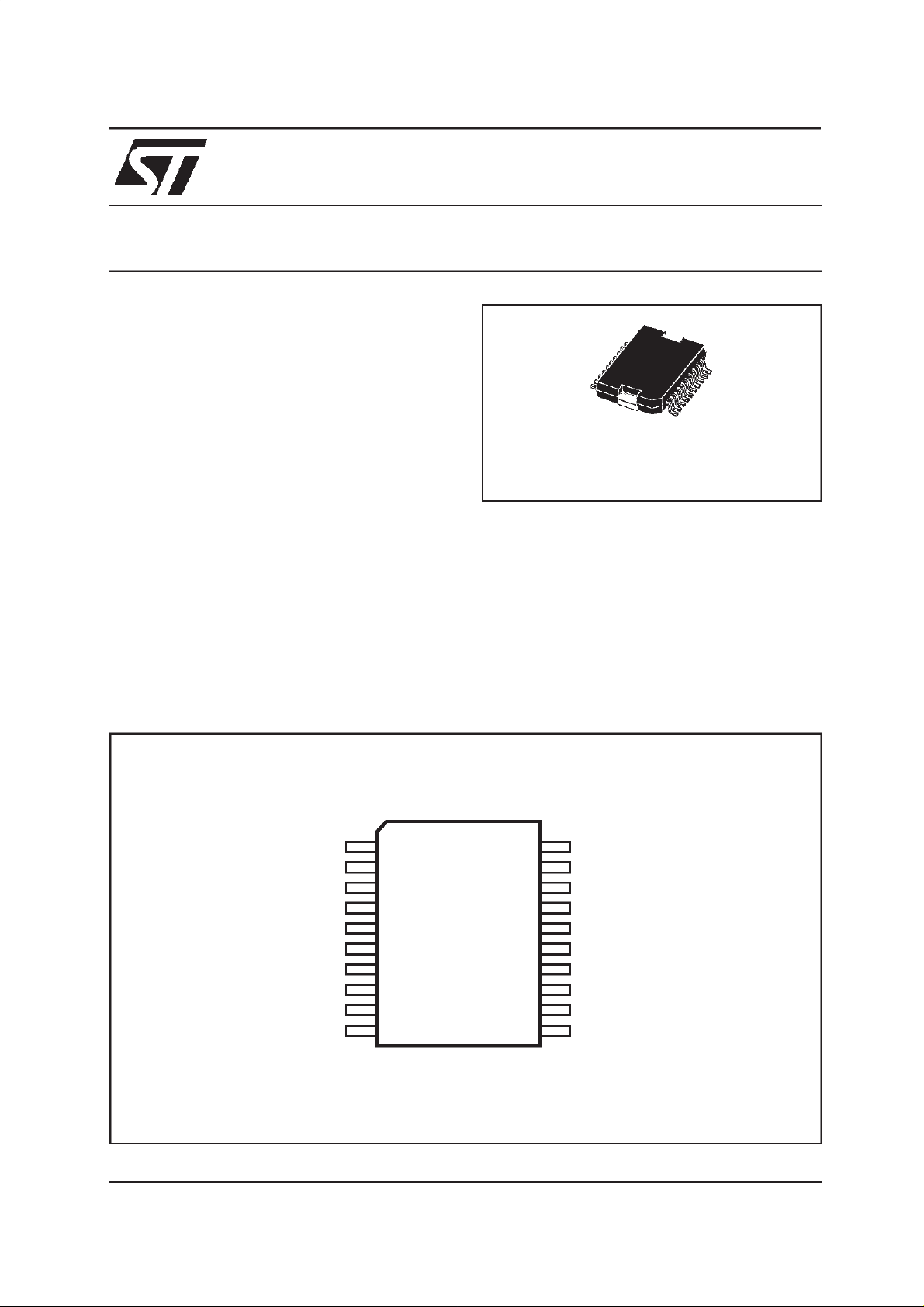
L4 937N PD
PowerSO20
ORDERINGNUMBER: L4937NPD
DESCRIPTION
TheL4937NPDisa monolithicintegrateddualvoltage regulators with two very low dropout outputs
andadditionalfunctionssuchaspower-onresetand
inputvoltagesense.Theyaredesignedfor supplying microcomputer controlled systems specially in
automotiveapplications.
PI N CONNEC TIO N
(top view)
GND
N.C.
GND
N.C.
CT
EN
N.C.
GND 10
1
2
V
S
V
S
3
4
5
6
7
8
9
D95AT162A
20
19
18
17
16
15
14
13
12
11
GND
N.C.
V
O2
N.C.
V
O1
GND
RESET
N.C.
N.C.
GND
June 2000
This is advanced information on a new product now in development or undergoing evaluation. Details are subject to change without notice.
1/9
Page 2
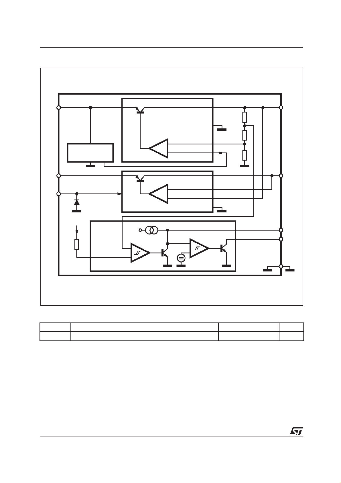
L4937NPD
BLOCK DIAGRAM
V
V
EN
S1
S2
1.23V
REFERENCE
RESET
REG1
REG2
2µ
2.0V
1.23V
V
O1
V
O2
CT
RES
GND
D95AT163
THERMAL DATA
Symbol Parameter Value Unit
2/9
R
thj-case
ThermalResistance Junction-Case Max. 1.5
C/W
°
Page 3
L4937NPD
ABSOLUTE MAXIMUM RATINGS
Symbol Parameter Value Unit
V
T
j,Tstg
I
EN
V
EN
V
RES
I
RES
P
The circuit is ESD protected according to MIL–STD–883C.
Note :
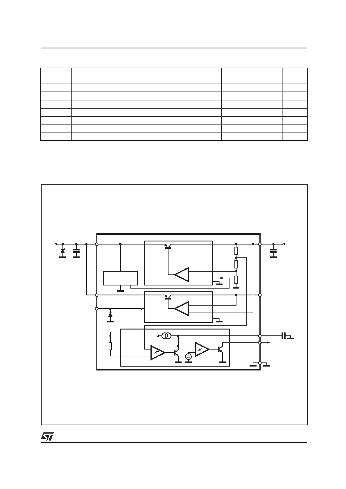
APPLI CATI ON CI R CUIT
DC Supply Voltage 28 V
S
TransientSupply Voltage(T < 1s) 40 V
Junctionand Storage TemperatureRange –55 to 150
Enable Input Current(V
EN
0.3V)
≤
Enable Input Voltage V
1
±
S
Reset OutputVoltage 20 V
Reset OutputCurrent 5 mA
Power Dissipation 875 mW
D
°
mA
C
V
S1
C
S
REFERENCE
V
S2
EN
1.23V
RESET
REG1
REG2
2µ
CS≥ 1µF;C01≥ 6µF;C02≥ 10µF, ESR < 10Ω at 10KHz
2.0V
1.23V
D95AT164
V
O1
V
O2
CT
RES
GND
C
O1
CT
3/9
Page 4

L4937NPD
ELECTRICAL CHARACTERISTICS (VS= 14V; –40°C ≤ TJ≤ 125°C unlessotherwise specified)
Symbol Parameter Test Conditions Min. Typ. Max. Unit
V
V
V
O2-VO1
V
DP1
V
V
DP2
V
V
OL 1.2
V
OLO1
V
OLO2
I
LIM1
I
LIM2
I
QSB
I
Operating Supply Voltage 25 V
S
StandbyOutput Voltage
O1
Output Voltage 2 TrackingError
6V ≤ V
1mA≤I
6V≤V
5mA≤I
≤ 25V
S
O1
≤
S
O2
50mA
≤
25V
500mA
≤
4.90 5.00 5.10 V
–25 +25 mV
Enable= LOW
DropoutVoltage1 IO1= 10mA
Inputto OutputVoltage
IO1
I
= 50mA
O1
Vs = 4V, IO1= 35mA 0.4 V
0.1
0.2
Differencein Undervoltage
Condition
DropoutVoltage2 IO1 = 100mA
Inputto OutputVoltage
IO2
I
= 500mA
O1
Vs = 4.6V,IO1= 350mA 0.6 V
0.2
0.3
Differencein Undervoltage
Condition
LineRegulation
6V ≤ V
I
Load Regulation 1
Load Regulation 2
1mA≤I
5mA≤I
Current Limit 1 VO1= 4.5V
V
≤ 25V
S
= 1mA; IO2= 5mA
O1
50mA
≤
O1
500mA
≤
O2
= 0V(note1)
O1
55
25
100
50
Current Limit 2 VO2= 0V 550 1000 1700 mA
Quiescent Current StandbyMode
(output2 disabled)
Quiescent Current IO1= 50mA
Q
I
= 0.3mA;TJ< 100°C
O1
2.4V
V
≥
EN
V
= 14V
S
V
= 3.5V
S
I
= 500mA
O1
210
340
0.25
0.4
0.3
0.6
20 mV
25 mV
50 mV
200
100
290
850
30 mA
V
V
V
V
mA
mA
µ
µA
A
ENABLE
V
ENL
V
ENH
V
ENhyst
I
EN
4/9
EnableInputLOW Voltage
–0.3 1.5 V
(output2 active)
EnableInputHIGH Voltage 2.4 7 V
EnableHysteresis 30 75 200 mV
EnableInputCurrent 0V < VEN< 1.2V
2.5V < V
EN
<7V
–10–1–1.50–0.5
+1
µ
µ
A
A
Page 5

L4937NPD
ELECTRICAL CHARACTERISTICS (continued)
RESET
Symbol Parameter Test Conditions Min. Typ. Max. Unit
V
V
t
RD
t
RR
V
I
LRES
V
CTh
V
CTh, hyst
Note : 1: Foldbackcharacteristic
ResetLow Threshold Voltage Vo1-0.4 4.7 Vo1-0.1 V
Rt
ResetThreshold Hysteresis 50 100 200 mV
Rth
ResetPulseDelay
ResetReactionTime CT= 100nF 1 10 50
ResetOutputLOW Voltage
RL
ResetOutputHIGH Leakage V
Delay Comparator Threshold 2.0 V
Delay Comparator Threshold
Hysteresis
= 100nF;tR> 100µs
C
T
= 10KΩtoV
R
RES
VS= 1.5V
=5V 1 µ
RES
01
55 100 180 ms
100 mV
0.4 V
µs
A
FUNCTI O NAL DES CRIPTIO N
TheL4937NDisbasedontheSGS-THOMSONMicroelectronicsmodularvoltageregulatorapproach.
Several out-standing features and auxiliary functionsareprovidedto meettherequirementsof supplyingthemicroprocessorsystemsusedinautomotiveapplications.
Furthermorethe device is suitablealso in otherapplications requiringtwostabilizedvoltages.
The modular approach allows other features and
functionsto berealized easilywhenrequired.
STANDBYREGULATOR
The standby regulator uses an Isolated Collector
Vertical PNP transistor as the regulating element.
This structureallows a verylow dropoutvoltageat
currentsup to 50mA. The dropoutoperationofthe
standby regulator is maintained down to 2V input
supplyvoltage.The output voltage is regulatedup
tothetransientinputsupplyvoltageof40V.Thisfeatureavoidsfunctionalinterruptions whichcouldbe
generatedby overvoltagepulses.
Figure1 :
OutputVoltagevs. Input Voltage.
Thetypicalcurveof thestandbyoutputvoltageasa
functionof theinputsupplyvoltageisshowninfig.1.
The current consumption of the device (quiescent
current) is less than 260µA when output 2 is disabled(standbymode).The dropoutvoltageis controlledto reducethe quiescentcurrentpeak in the
undervoltage region and to improve the transient
responsein thisregion.
Thequiescentcurrentisshowninfig.2asafunction
of the supplyinputvoltage2.
OUTPUT2 VOLTAGE
Theoutput2regulatorusesthe same outputstruc-
tureasthestandbyregulator,butratedforanoutput
currentof500mA.
The output2 regulatorworks in trackingmode with
the standbyoutput voltage as a referencevoltage
when theoutput2.
The output 2 regulator can be switched off via the
Enableinput.
5/9
Page 6

L4937NPD
Figure2 : QuiescentCurrent vs. SupplyVoltage.
400µ
200µ
Figure3 : ProgrammableOutput2 VoltagewithExternalResistors.
RESETCIRCUIT
Theblockcircuitdiagramoftheresetcircuitisshown
infig.4.Theresetcircuitsupervisesthestandbyoutput voltage.The reset threshold of 4.7V is defined
by the internal reference voltage and the standby
outputdivider.
The reset pulse delay time t
chargetime of an externalcapacitorC
x2V
C
T
=
t
RD
6/9
2µA
, is defined by the
RD
:
T
Thereactiontimeoftheresetcircuitdependsonthe
discharge time limitation of the reset capacitor C
and is proportionalto the valueof CT.
The reactiontime of the resetcircuit increasesthe
noiseimmunity.Infact,if thestandbyoutputvoltage
drops below the resetthresholdfor a time shorter
thanthereactiontime t
, noresetoutputvariation
RR
occurs. The nominal reset delay is generated for
standbyoutput voltage drops longer than the time
necessary for the complete dischargingof the capacitorC
C
T
. This time is typically equal to 50µsif
T
=100nF.Thetypicalresetoutputwaveformsare
shownin fig.5.
T
Page 7

L4937NPD
Figure4 :
BlockDiagramoftheResetCircuit.
Figure 5 : TypicalResetOutputWaveforms.
VOUT1
VRT +0.2V
VRT
1.5V
RESET
t
RD
VINPUT
VOUT1
t
RR
t
R
t
RD
D95AT216
7/9
Page 8

L4937NPD
DIM.
MIN. TYP. MAX. MIN. TYP. MAX.
mm inch
A 3.6 0.142
a1 0.1 0.3 0.004
0.012
a2 3.3 0.130
a3 0 0.1 0.000 0.004
b 0.4 0.53 0.016 0.021
c 0.23 0.32 0.009 0.013
D (1) 15.8 16 0.622 0.630
D1 9.4 9.8 0.370 0.386
E 13.9 14.5 0.547 0.570
e 1.27 0.050
e3 11.43 0.450
E1 (1) 10.9 11.1 0.429 0.437
E2 2.9
0.114
E3 5.8 6.2 0.228 0.244
G 0 0.1 0.000 0.004
H 15.5 15.9 0.610 0.626
h 1.1
0.043
L 0.8 1.1 0.031 0.043
N10°(max.)
S
8°(max.)
T 10 0.394
(1) ”Dand F” donot includemold flash or protrusions.
- Moldflash or protrusions shall notexceed 0.15mm (0.006”).
- Criticaldimensions: ”E”,”G” and ”a3”
OUTLINE AND
MECHANICAL DATA
JEDEC MO-166
PowerSO20
E2
hx
45
DETAIL B
BOTTOM VIEW
R
lead
a3
Gage Plane
E
DETAIL B
0.35
S
D1
a1
L
c
DETAIL A
slug
-C-
SEATING PLANE
GC
(COPLANARITY)
E3
NN
a2
A
b
DETAIL A
e3
H
D
T
1
e
1120
E1
10
PSO20MEC
8/9
Page 9

L4937NPD
Information furnished is believed to be accurate and reliable. However, STMicroelectronics assumes no responsibility for the consequences of use of such information nor for any infringement of patents or other rights of third parties which may result from its use. No
license is granted by implication or otherwise under any patent or patent rights of STMicroelectronics. Specification mentioned in this
publication are subject to change without notice. This publication supersedes and replaces all information previously supplied. STMicroelectronics products are not authorized for use as critical components in life support devices or systems without express written
approval of STMicroelectronics.
Australia - Brazil - China - Finland - France - Germany - Hong Kong - India - Italy - Japan - Malaysia - Malta - Morocco -
The ST logo is a registered trademark of STMicroelectronics
2000 STMicroelectronics – Printedin Italy – All Rights Reserved
STMicroelectronics GROUP OF COMPANIES
Singapore - Spain - Sweden - Switzerland - United Kingdom - U.S.A.
http://www.st.com
9/9
 Loading...