

Page 1
DUAL MULTIFUNCTIONVOLTAGE REGULATOR
.
STANDBYOUTPUTVOLTAGEPRECISION5V
± 2%
.
OUTPUT2TRACKEDTOTHESTANDBYOUTPUT
.OUTPUT 2 DISABLE FUNCTION FOR
STANDBYMODE
.VERY LOW QUIESCENT CURRENT, LESS
THAN250µA,IN STANDBYMODE
.OUTPUTCURRENTS: I
.
VERYLOW DROPOUT(max 0.4V/0.6V)
=50mA,I02=500mA
01
.OPERATINGTRANSIENTSUPPLYVOLTAGE
UP TO 40V
.POWER-ON RESET CIRCUIT SENSING THE
STANDBYOUTPUTVOLTAGE
.POWER-ONRESET DELAYPULSEDEFINED
BY THEEXTERNALCAPACITOR
.
THERMALSHUTDOWNANDSHORTCIRCUIT
PROTECTIONS
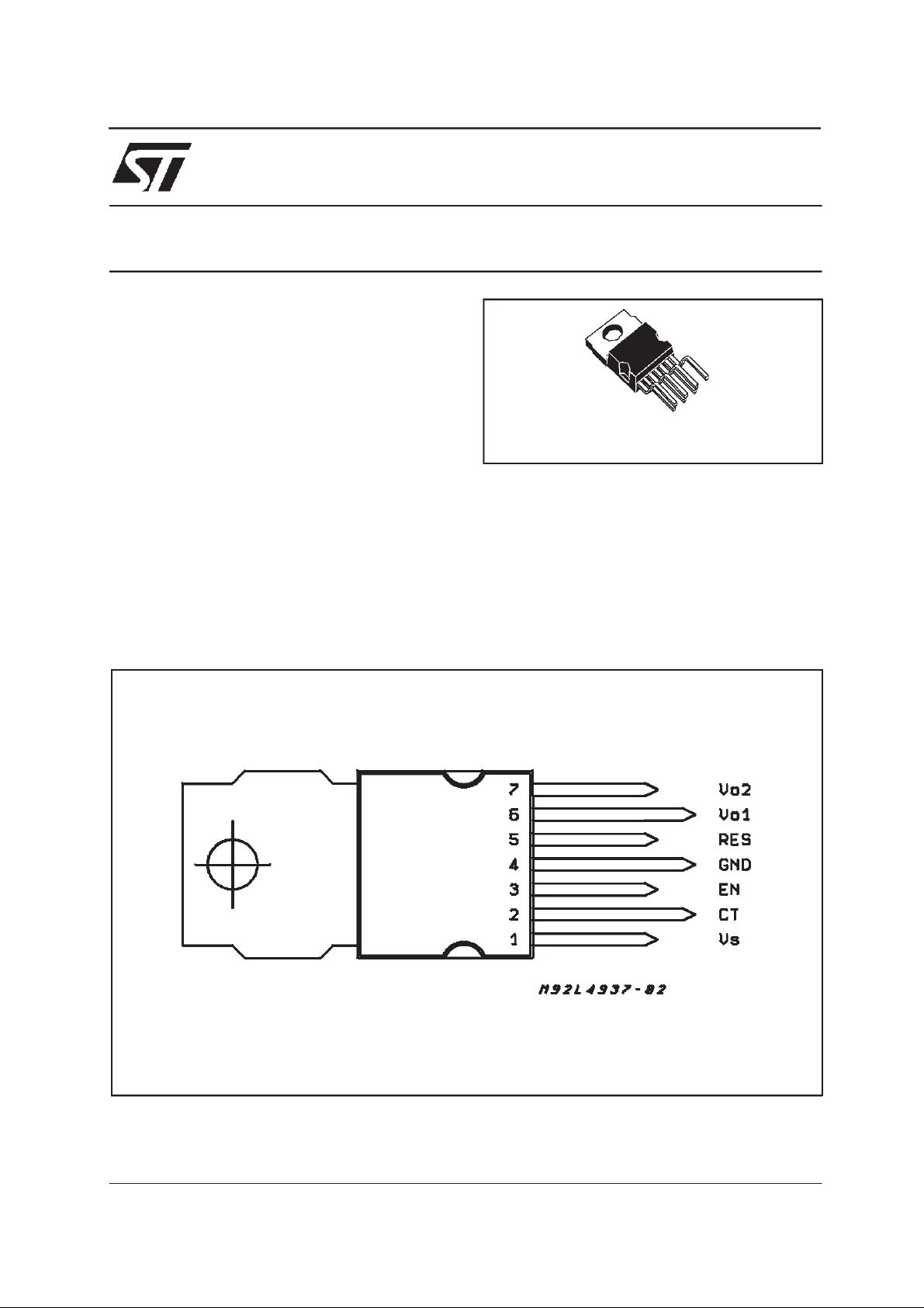
L4937N
Heptawatt
ORDERING NUMBER : L4937N
DES CRIP T ION
TheL4937Nis amonolithicintegrateddual voltage
regulatorswithtwoverylowdropoutoutputsandadditionalfunctionssuch as power-onresetand input
voltage sense. It is designed for supplying microcomputer controlled systems specially in automotiveapplications.
PIN CONNECTI ON
(top view)
June 2000
1/9
Page 2
L4937N
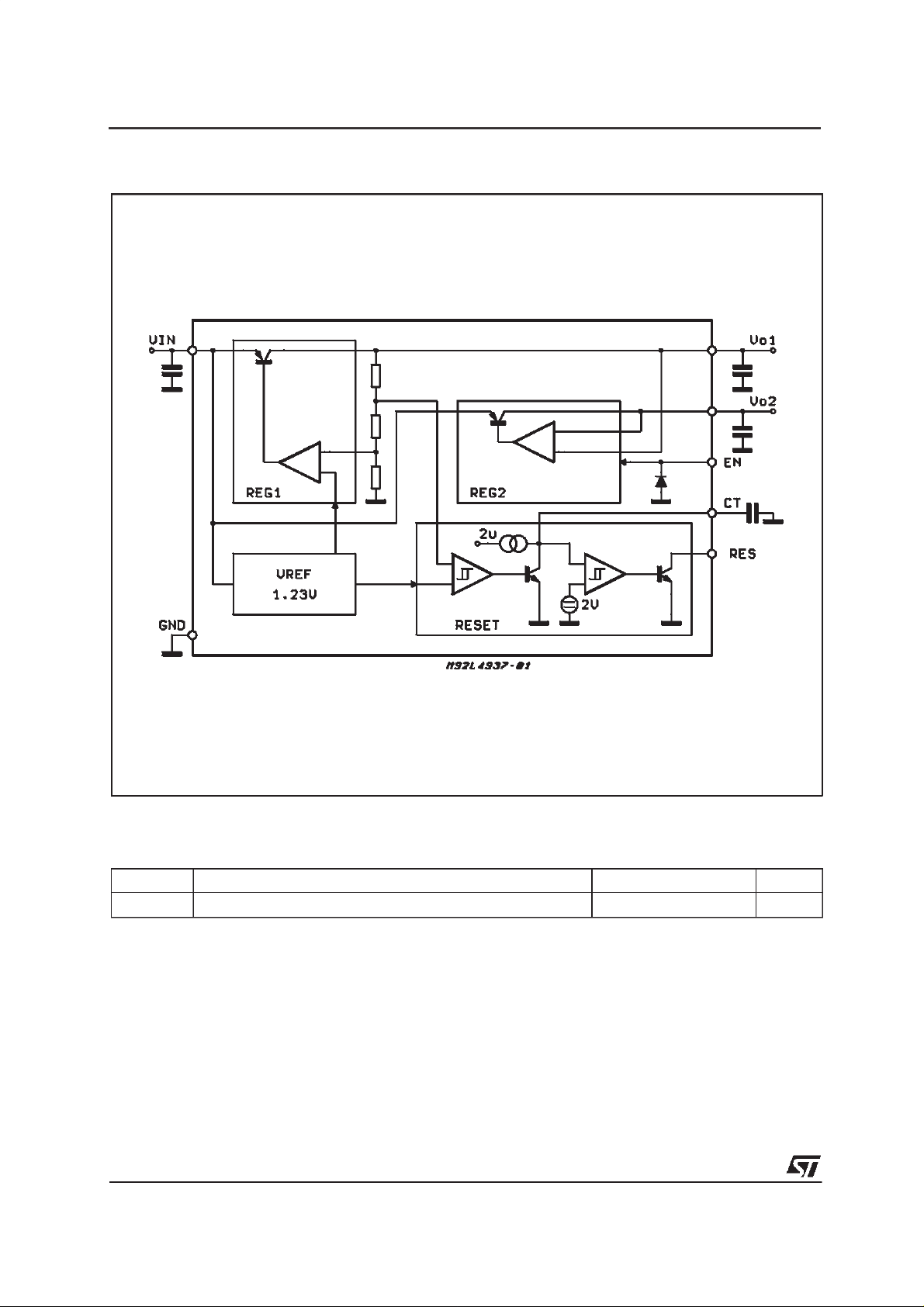
BLOCK DIAGRAM
THERMAL DATA
Symbol Parameter Value Unit
2/9
R
thj-case
Thermal Resistance Junction-Case Max. 3
C/W
°
Page 3
ABSOLUTE MAXIMUM RATINGS
Symbol Parameter Value Unit
V
DC Supply Voltage 28 V
S
Transient Supply Voltage (T < 1s) 40 V
T
j,Tstg
I
EN
V
EN
V
RES
I
RES
P
Note : The circuit is ESD protected according to MIL–STD–883C.
Junction and Storage Temperature Range –55 to 150
Enable Input Current (V
EN
0.3V)
≤
Enable Input Voltage V
1
±
S
Reset Output Voltage 20 V
Reset Output Current 5 mA
Power Dissipation (TA=80°C, R
D
th heatsink
=9°C/W)
5W
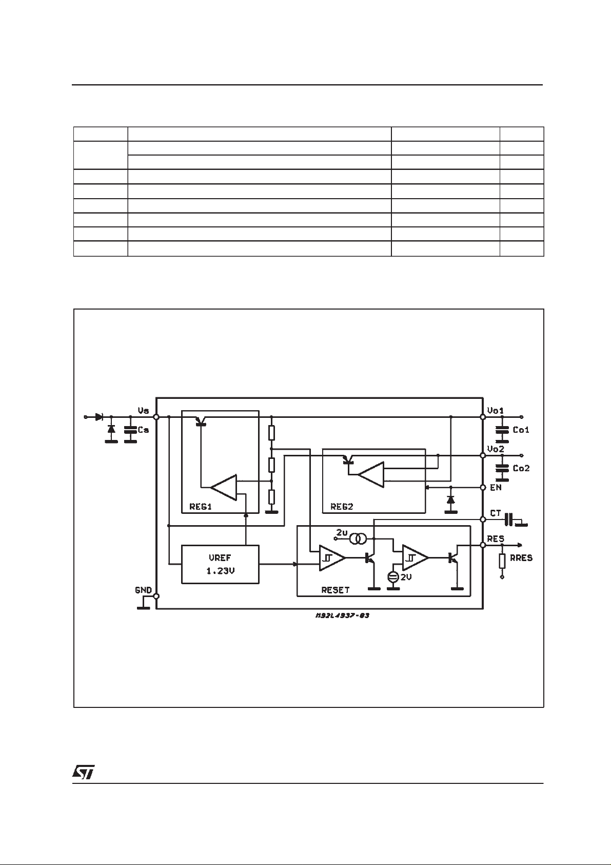
APP LICATIO N CIRCUIT
L4937N
C
°
mA
CS≥ 1µF;C01≥ 6µF;C02≥ 10µF, ESR < 10Ω at 10KHz
3/9
Page 4

L4937N
ELECTRICAL CHARACTERISTICS (VS= 14V; –40°C ≤ Tj≤ 125°C unless otherwise specified)
Symbol Parameter Test Conditions Min. Typ. Max. Unit
V
V
V
O2-VO1
V
DP1
V
V
DP2
V
V
OL1.2
V
OLO1
V
OLO2
I
LIM1
I
LIM2
I
QSB
I
Operating Supply Voltage 25 V
S
Standby Output Voltage
O1
Output Voltage 2 Tracking Error
(note 1)
6V≤V
1mA≤I
6V≤V
5mA ≤ I
≤
S
≤
O1
≤
S
≤ 500mA
O2
25V
50mA
25V
4.90 5.00 5.10 V
–25 +25 mV
Enable = LOW
Dropout Voltage 1 IO1= 10mA
Input to Output Voltage
IO1
= 50mA
I
O1
VS = 4V, IO1= 35mA 0.4 V
0.1
0.2
Difference in Undervoltage
Condition
Dropout Voltage 2 IO2 = 100mA
Input to Output Voltage
IO2
= 500mA
I
O2
VS = 4.6V, IO2= 350mA 0.6 V
0.2
0.3
Difference in Undervoltage
Condition
Line Regulation
Load Regulation 1
Load Regulation 2
6V ≤ V
I
O1
1mA≤I
5mA≤I
Current Limit 1 VO1= 4.5V
V
O1
≤ 25V
S
= 1mA; IO2= 5mA
50mA
≤
O1
500mA
≤
O2
= 0V (note 2)
55
25
100
50
Current Limit 2 VO2 = 0V 550 1000 1700 mA
Quiescent Current Standby
Mode (output 2 disabled)
Quiescent Current IO1= 50mA
Q
= 0.3mA; TJ< 100°C
I
O1
2.4V
V
≥
EN
= 14V
V
S
= 3.5V
V
S
= 500mA
I
O1
210
340
0.25
0.4
0.3
0.6
20 mV
25 mV
50 mV
200
100
290
850
30 mA
V
V
V
V
mA
mA
µ
µ
A
A
ENABLE
V
ENL
V
ENH
V
ENhyst
I
EN
4/9
Enable Input LOW Voltage
–0.3 1.5 V
(output 2 active)
Enable Input HIGH Voltage 2.4 7 V
Enable Hysteresis 30 75 200 mV
Enable Input Current 0V < VEN< 1.2V
2.5V < V
EN
<7V
–10–1–1.50–0.5
+1
µ
µ
A
A
Page 5

L4937N
ELECTRICAL CHARACTERISTICS
(continued)
RESET
Symbol Parameter Test Conditions Min. Typ. Max. Unit
V
V
t
RD
t
RR
V
I
LRES
V
CTth
V
CTth,hyst
Note :
FUNCTI ON AL DESCRIPTION
The L4937Nis based on the SGS-THOMSON Microelectronicsmodularvoltageregulatorapproach.
Several out-standing features and auxiliary functionsareprovidedtomeet therequirementsof supplyingthemicroprocessorsystemsusedinautomotiveapplications.
Furthermorethedevice issuitablealso inother applicationsrequiringtwo stabilizedvoltages.
The modular approach allows other features and
functionsto be realizedeasilywhen required.
STANDBYREGULATOR
The standby regulator uses an Isolated Collector
Vertical PNP transistor as the regulatingelement.
This structure allowsa verylow dropout voltageat
currentsup to 50mA. The dropout operationof the
standby regulator is maintained down to 2V input
supply voltage. The outputvoltage is regulatedup
tothetransientinputsupplyvoltageof40V.Thisfeature avoids functionalinterruptions which could be
Reset Low Threshold Voltage VS= 14V Vo1-0.4 4.7 Vo1-0.1 V
Rt
Reset Threshold Hysteresis 50 100 200 mV
Rth
Reset Pulse Delay
Reset Reaction Time CT= 100nF 1 10 50
Reset Output LOW Voltage
RL
Reset Output HIGH Leakage V
Delay Comparator Threshold 2.0 V
Delay Comparator Threshold
Hysteresis
1:V
connected to ADJ.VO2canbe set to higher values by inserting an external resistordivider.
O2
2 : Foldback characteristic
= 100nF; tR> 100µs
C
T
= 10KΩto V01V
R
RES
=5V 1
RES
1.5V
≥
S
55 100 180 ms
100 mV
The typicalcurve of the standby outputvoltage as
afunctionof theinputsupplyvoltageis shownin fig.
1.
The current consumptionof the device (quiescent
current) is less than 250µA when output 2 is disabled(standbymode).The dropoutvoltage is controlled to reduce the quiescent current peak in the
undervoltage regionand to improve the transient
responsein this region.
Thequiescentcurrentisshowninfig.2 asafunction
of thesupplyinput voltage2.
OUTPUT2 VOLTAGE
Theoutput2 regulatorusesthe same outputstruc-
tureas thestandbyregulator,butratedforanoutput
currentof 500mA.
Theoutput 2 regulatorworks in trackingmode with
the standbyoutputvoltageas a referencevoltage.
The output 2 regulator can be switched off via the
Enableinput.
0.4 V
generatedby overvoltagepulses.
s
µ
A
µ
5/9
Page 6

L4937N
Figure1 : OutputVoltagevs. InputVoltage.
Figure2 : QuiescentCurrent vs.SupplyVoltage.
400
200
RESETCIRCUIT
Theblockcircuitdiagramof theresetcircuitisshown
infig.3.Theresetcircuitsupervisesthestandbyoutput voltage. The reset threshold of 4.7V is defined
by the internal reference voltage and the standby
outputdivider.
The reset pulse delay time t
chargetime ofan externalcapacitorC
C
x2V
T
=
t
RD
2µA
, is defined by the
RD
:
T
Thereactiontimeof theresetcircuitdependsonthe
discharge time limitation of the reset capacitor C
and isproportionalto thevalue of CT.
The reactiontime of the reset circuit increasesthe
noiseimmunity.Infact,ifthestandbyoutputvoltage
drops below the reset threshold for a time shorter
thanthe reactiontimet
, noreset outputvariation
RR
occurs. The nominal reset delay is generated for
standbyoutputvoltage drops longer than the time
necessaryfor the complete discharging of the capacitorC
. This timeis typicallyequalto 50µsifC
T
= 100nF. The typical reset output waveforms are
shownin fig.
T
T
6/9
Page 7

L4937N
Figure3 :
Figure4 :
BlockDiagramof theReset Circuit.
TypicalReset OutputWaveforms.
VRT
VOUT1
+0.2V
VRT
1.5V
RESET
t
RD
VINPUT
VOUT1
t
RR
t
R
t
RD
D95AT216
7/9
Page 8

L4937N
DIM.
MIN. TYP. MAX. MIN. TYP. MAX.
A 4.8 0.189
C 1.37 0.054
D 2.4 2.8 0.094 0.110
D1 1.2 1.35 0.047 0.053
E 0.35 0.55 0.014 0.022
E1 0.7 0.97 0.028 0.038
F 0.6 0.8 0.024 0.031
F1 0.9 0.035
G 2.34 2.54 2.74 0.095 0.100 0.105
G1 4.88 5.08 5.28 0.193 0.200 0.205
G2 7.42 7.62 7.82 0.295 0.300 0.307
H2 10.4
H3 10.05 10.4 0.396 0.409
L 16.7 16.9 17.1 0.657 0.668 0.673
L1 14.92
L2 21.24 21.54 21.84 0.386 0.848 0.860
L3 22.27 22.52 22.77 0.877 0.891 0.896
L4 1.29
L5 2.6 2.8 3 0.102 0.110 0.118
L6 15.1 15.5 15.8 0.594 0.610 0.622
L7 6 6.35 6.6 0.236 0.250 0.260
L9 0.2 0.008
M 2.55 2.8 3.05 0.100 0.110 0.120
M1 4.83 5.08 5.33 0.190 0.200 0.210
V4 40° (typ.)
Dia 3.65 3.85 0.144 0.152
mm inch
0.409
0.587
0.051
OUTLINE AND
MECHANICAL DATA
Heptawatt V
H3
L
VV
E
L1
M1
A
C
D
M
D1
H2
V4
L9
H1
L5
Dia.
L2
L3
F
E1
E
GG1G2
F
L7
L4
L6
F1H2
HEPTAMEC
8/9
Page 9

L4937N
Information furnished is believed to be accurate and reliable. However, STMicroelectronics assumes no responsibility for the consequences of use of such information nor for any infringement of patents or other rights of third parties which may result from its use. No
license is granted by implication or otherwise under any patent or patent rights of STMicroelectronics. Specification mentioned in this
publication are subject to change without notice. This publication supersedes and replaces all information previously supplied. STMicroelectronics products are not authorized for use as critical components in life support devices or systems without express written
approval of STMicroelectronics.
Australia - Brazil - China - Finland - France - Germany - Hong Kong - India - Italy - Japan - Malaysia - Malta - Morocco -
The ST logo is a registered trademark of STMicroelectronics
2000 STMicroelectronics – Printed in Italy – All Rights Reserved
HEPTAWATT is a Trademark of STMicroelectronics
STMicroelectronics GROUP OF COMPANIES
Singapore - Spain - Sweden - Switzerland - United Kingdom - U.S.A.
http://www.st.com
9/9
 Loading...