

Page 1
DUAL 5V REGULATOR WITH RESETAND DISABLE
.
DOUBLEBATTERYOPERATING
.
OUTPUTCURRENTS : I01=300 mA
= 300 mA
I
02
.
FIXED PRECISIONOUTPUT VOLTAGE
5V±
2
%
.
RESETFUNCTION CONTROLLED BY INPUT
VOLTAGEANDOUTPUT1 VOLTAGE
.
RESET FUNCTION EXTERNALLY PROGRAMMABLETIMING
.
RESET OUTPUT LEVEL RELATED TO OUTPUT 2
.
OUTPUT 2 INTERNALLY SWITCHED WITH
ACTIVEDISCHARGING
.
OUTPUT2 DISABLELOGICALINPUT
.
LOW LEAKAGE CURRENT, LESS THAN 1µA
ATOUTPUT1
.
RESETOUTPUT NORMALLY HIGH
.
INPUT OVERVOLTAGE PROTECTION UP TO
60V
.
OUTPUTTRANSISTORS SOA PROTECTION
.
SHORT CIRCUIT AND THERMAL OVERLOADPROTECTION
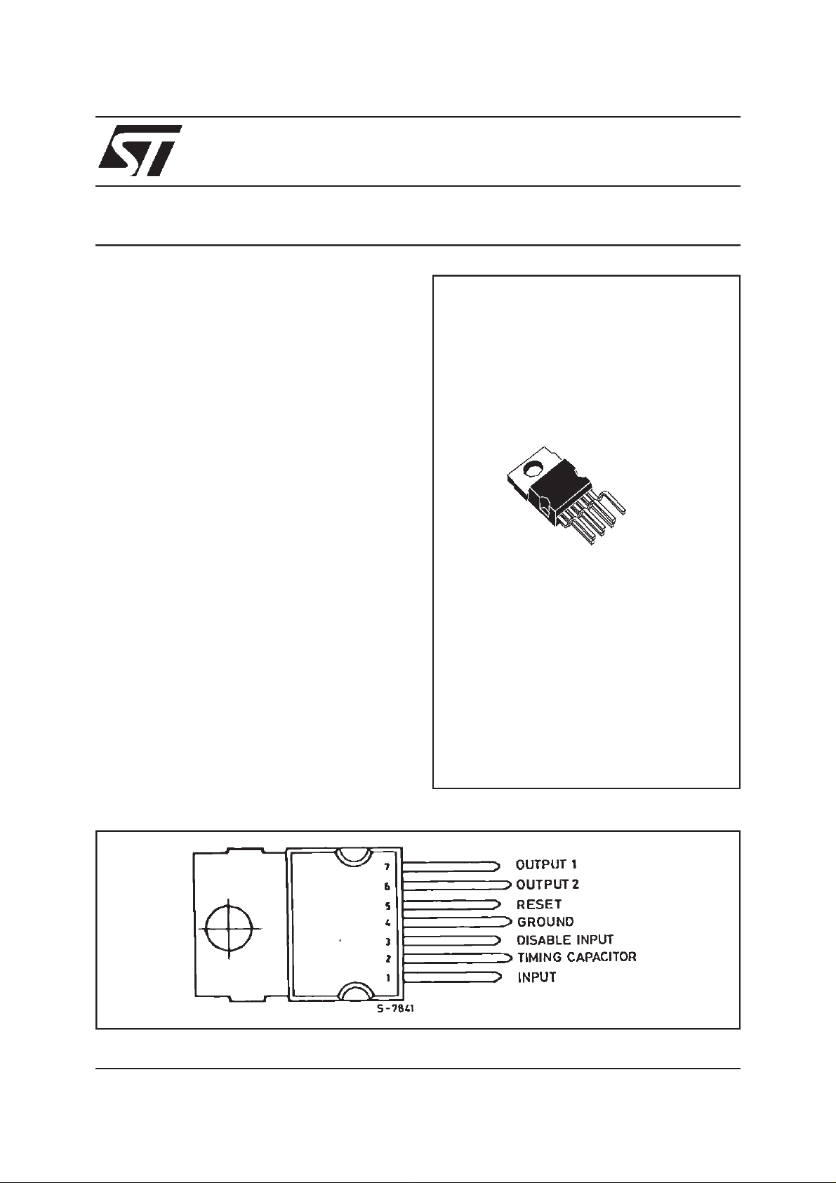
L4902A
HEPTAWATT
ORDERING NUMBER : L4902A
(Vertical)
DESCRIPTION
The L4902A is a monolithic low drop dual 5V
regulatordesignedmainlyfor supplying microprocessorsystems.
Reset and data save functions and remoteswitch
on/offcontrol can be realized.
PIN CONNECTION
June 2000
1/9
Page 2
L4902A
PIN FUNCTIONS
N°
1 Input 1 Regulators Common Input
2 Timing
3 Disable Input A high level (> V
4 GND Common Ground
5 Reset Output When pin 2 reaches 5V the reset output is switched high.
6 Output 2 5V – 300mA Regulator Output. Enabled if V
7 Output 1 5V – 300mA. Low leakage (in switch-OFF condition) output
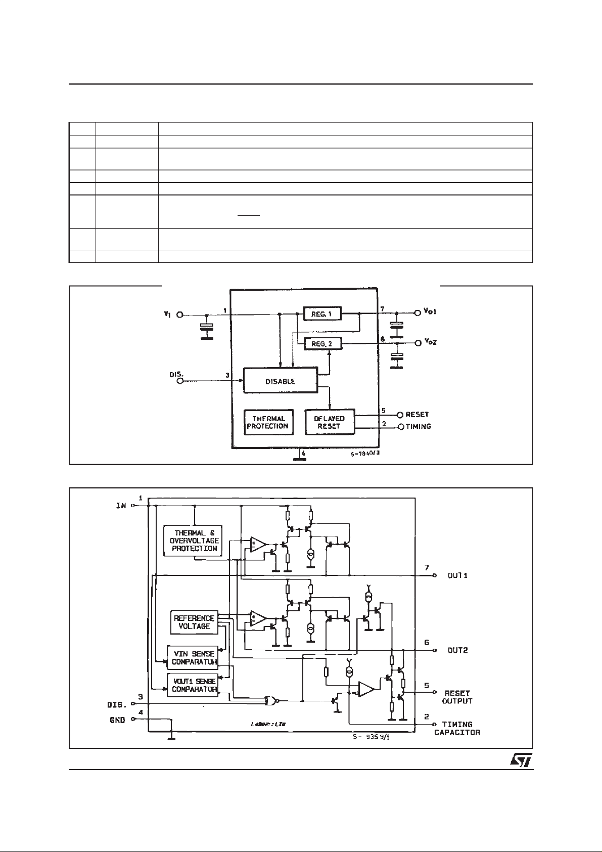
BLOCKDIAGRAM
Name Function
If Reg. 2 is switched-ON thedelay capacitor is charged with a5µA constant current. When
Capacitor
Reg. 2 is switched-OFF the delay capacitor is discharged.
) disable outputReg. 2.
DT
5V
(
Therefore t
RD=Ct
Reg. 2 is switched-OFF the C
);tRD(ms) = Ct(nF)
10µA
capacitor is discharged.
02
1>VRT. DISABLE INPUT < VDTand VIN>VIT.If
o
SCHEMATIC DIAGRAM
2/9
Page 3
L4902A
ABSOLUTE MAXIMUMRATINGS
Symbol Parameter Value Unit
V
I
T
stg,Tj
IN
o
DC Input Voltage
Transient Input Overvoltage(t = 40ms)
Output Current Internally Limited
Storage and Junction Temperature – 40 to 150
THERMAL DATA
Symbol Parameter Value Unit
R
th j-case
Thermal Resistance Junction-case Max 4
28
60
V
V
°C
°C/W
ELECTRICAL CHARACTERISTICS
(V
IN
= 14.4V,T
=25oC unless otherwise specified))
amb
Symbol Parameter Test Conditions Min. Typ. Max. Unit
V
DC Operating Input Voltage 24 V
i
V
V
V
I
I
L01
I
V
V
V
∆V
∆V
∆V
∆V
V
V
V
V
t
V
∆V
∆
∆V
∆
SVR1 Supply Voltage Rejection f = 100Hz V
Output Voltage 1
01
Output Voltage 2 HIGH
02 H
Output Voltage 2 LOW I02= – 5mA 0.1 V
02 L
Output Current 1 max.
01
Leakage Output 1 Current
Output Current 2 max.
02
Output 1 Dropout Voltage (*) I01= 10mA
i01
Input Threshold Voltage V01+ 1.2 6.4 V01+ 1.7 V
IT
Input Threshold VoltageHyst. 250 mV
iTH
Line Regulation 1 7V < VIN< 24V,I01= 5mA 5 50 mV
01
Line Regulation 2 7V < VIN< 24V,I02= 5mA 5 50 mV
02
Load Regulation 1 5mA < I01< 300mA 40 80 mV
01
Load Regulation 2 5mA < I02< 300mA 50 80 mV
02
Quiescent Current
I
Q
Reset Threshold Voltage V02– 0.15 4.9 V02– 0.05 V
RT
Reset Threshold Hysteresis 30 50 80 mV
RTH
Reset Output Voltage HIGH
RH
Reset Output Voltage LOW IR= – 1mA 0.25 0.4 V
RL
Reset Pulse Delay Ct= 10nF 3 5 11 ms
RD
t
Timing Capacitor Discharge Time Ct= 10nF 20
d
V02Disable Threshold Voltage 1.25 2.4 V
DT
I
V02Disable Input Current
D
01
Thermal Drift
T
02
Thermal Drift
T
R Load 1k
R Load 1k
= – 100mV
∆V
01
=0,V01≤ 3V
V
IN
= – 100mV
∆V
02
= 100mA
I
01
= 300mA
I
01
I
0<V
7V < V
7V < V
I
V
V
01=I02
= 500µA
R
≤ 0.4V
D
≥ 2.4V
D
≤
< 13V
IN
< 13V V02LOW
IN
< 13V V02HIGH
IN
–20°C≤T
–20°C≤T
Io = 100mA
Ω 4.95 5.05 5.15 V
Ω V
–0.1 5 V
01
300 mA
300 mA
0.7
0.8
1.1
5mA
4.5
2.7
1.6
V
– 1 4.12 V
02
– 150
–30
amb
amb
R
≤125°C
≤125°C
= 0.5V
50 84 dB
0.3
– 0.8
0.3
– 0.8
1
0.8
1
1.4
6.5
4.5
3.5
01
V
µA
V
V
V
mA
02
V
µs
µA
µA
mV/°C
mV/°C
SVR2 Supply Voltage Rejection 50 80 dB
* The dropoutvoltage is defined as thedifference between theinput and the outputvoltage when theoutputvoltage is lowered of 25mV under
constant output current condition.
3/9
Page 4

L4902A
TESTCIRCUIT
APPLICATIONINFORMATION
InpowersuppliesforµPsystemsit is necessaryto
provide power continuously to avoid loss of informationinmemoriesandin timeof dayclocks,or to
savedatawhen theprimarysupplyisremoved.The
L4902A makes it very easy to supplysuch equipments;it providestwo voltage regulators (both 5V
high precision) with common inputs plus a reset
output for the data save function and a Reg. 2
disableinput.
CIRCUITOPERATION (see Figure 1)
After switch on Reg. 1 saturates until V
rises to
01
the nominal value.
When the input reaches V
higherthan V
the reset output (V
theoutput2 (V02) switcheson and
RT
) also goes high after a pro-
R
and the output 1 is
IT
Figure1
grammabletime T
V
andVRareswitchedtogetherat lowlevelwhen
02
(timingcapacitor).
RD
one of the followingconditionsoccurs :
- a high level( V
) is applied on pin 3 ;
DT
- an input overvoltage;
- an overload on the output 1 (V
- a switch off (V
INVIT-VITH
);
01VRT
);
and theystart again as beforewhen the condition
is removed.
An overload on output 2 does not switch Reg. 2,
and does not influenceReg.1.
TheV
outputfeatures:
01
- 5V internal referencewithout voltage divider between the outputand theerror comparator
- very low drop series regulator element utilizing
current mirrors
permit high output impedance and then very low
leakagecurrent even in power down condition.
4/9
Page 5

L4902A
Thisoutputmaythereforebeusedtosupplycircuits
continuously, such as volatile RAMs, allowing the
useof a back-upbattery.
TheV
output can supply othernon essential5 V
02
circuits which may be powered down when the
system is inactive, or that must be powereddown
to preventuncorrect operationfor supply voltages
belowthe minimumvalue.
Theresetoutputcanbeusedas a”POWERDOWN
INTERRUPT”, permitting RAM access only in correctpowerconditions,orasa”BACK-UPENABLE”
to transfer data into in a NV SHADOW MEMORY
Figure2
when the supply is interrupted.
Thedisablefunctioncan be usedfor remoteon/off
controlof circuitsconnectedto theV
output.
02
APPLICATION SUGGESTIONS
Figure 2 illustrate how the L4902A’sdisable input
maybe used in a CMOSµComputerapplication.
TheV
regulator(lowconsumption)supplyperma-
01
nently a CMOS time of day clock and a CMOS
µcomputer chip with volatile memory. V
02
output,
supplyingnon-essentialcircuits,is turned OFFundercontrol of a
µPunit.
Figure3 :
P.C.Board Component Layoutof Figure 2
5/9
Page 6

L4902A
Configurations of this type are used in products
where the OFF switch is part of a keyboard
scanned by a micro which operates continuously
evenin the OFF state.
Anotherapplication for the L4902A is supplying a
shadow-rammicrocomputer chip (SGS M38SH72
forexample)where afastNV memoryisbackedup
onchipbyaEEPROMwhena lowlevelonthereset
output occurs.
By adding two CMOS-SCHMIDT-TRIGGER and
few external components, also a watch dog func-
Figure4
tionmaybe realized(see Figure5). During normal
operation the microsystem supplies a periodical
pulsewaveform;ifananomalousconditionoccours
(intheprogramorinthesystem),thepulseswillbe
absentand the disableinput will be activatedafter
a settlingtime determinedby R1 C1.In this condition all the circuitry connected to V
will be dis-
02
abled,the systemwillbe restartedwith a newreset
front.
Thedisableof V
preventspuriousoperationdur-
02
ing microprocessormalfunctioning.
Figure5
6/9
Page 7

L4902A
Figure6 : QuiescentCurrent versusOutput
ICurrent
Figure8 : Supply Voltage Rejection
Regulators1 and 2 versus Input Ripple Frequence
Figure7 : QuiescentCurrent versusInput Voltage
7/9
Page 8

L4902A
DIM.
MIN. TYP. MAX. MIN. TYP. MAX.
A 4.8 0.189
C 1.37 0.054
D 2.4 2.8 0.094 0.110
D1 1.2 1.35 0.047 0.053
E 0.35 0.55 0.014 0.022
E1 0.7 0.97 0.028 0.038
F 0.6 0.8 0.024 0.031
F1 0.9 0.035
G 2.34 2.54 2.74 0.095 0.100 0.105
G1 4.88 5.08 5.28 0.193 0.200 0.205
G2 7.42 7.62 7.82 0.295 0.300 0.307
H2 10.4 0.409
H3 10.05 10.4 0.396 0.409
L 16.7 16.9 17.1 0.657 0.668 0.673
L1 14.92
L2 21.24 21.54 21.84 0.386 0.848 0.860
L3 22.27 22.52 22.77 0.877 0.891 0.896
L4 1.29
L5 2.6 2.8 3 0.102 0.110 0.118
L6 15.1 15.5 15.8 0.594 0.610 0.622
L7 6 6.35 6.6 0.236 0.250
L9 0.2 0.008
M 2.55 2.8 3.05 0.100 0.110 0.120
M1 4.83 5.08 5.33 0.190 0.200 0.210
V4 40° (typ.)
Dia 3.65 3.85 0.144 0.152
mm inch
0.587
0.051
0.260
OUTLINE AND
MECHANICAL DATA
Heptawatt V
H3
L
VV
E
L1
M1
A
C
D
M
D1
H2
V4
L9
H1
L5
Dia.
L2
L3
F
E1
E
GG1G2
F
L7
L4
L6
F1H2
HEPTAMEC
8/9
Page 9

L4902A
Information furnished is believed to be accurate and reliable. However, STMicroelectronics assumes no responsibility for the
consequences of use of such information nor for any infringementof patents or other rights of third partieswhich may result from
its use. No license is granted by implication or otherwise under any patent or patent rights of STMicroelectronics. Specification
mentioned in this publication are subject to change without notice. This publication supersedes and replaces all information
previouslysupplied.STMicroelectronicsproducts arenot authorizedforuse ascriticalcomponents inlife supportdevices orsystems
without express written approval of STMicroelectronics.
Australia - Brazil - China - Finland- France - Germany - Hong Kong - India - Italy - Japan - Malaysia - Malta - Morocco -
The ST logo is a registered trademark of STMicroelectronics
2000 STMicroelectronics – Printed in Italy – All Rights Reserved
STMicroelectronics GROUP OF COMPANIES
Singapore- Spain - Sweden - Switzerland - UnitedKingdom - U.S.A.
http://www.st.com
9/9
 Loading...