

Page 1
L484
MAGNETIC PICKUP IGNITIONCONTROLLER
.DIRECT DRIVING OF THE EXTERNAL DAR-
LINGTON
.OPERATES WITH A WIDE RANGE OF MA-
GNETIC PICKUPTYPES
.CHARGINGANGLE(DWELL) CONTROL
.COILCURRENT PEAKLIMITATION
.CONTINUOUSCOILCURRENTPROTECTION
.TACHOMETER SIGNALOUTPUT
.EXTERNAL DARLINGTON OVERVOLTAGE
PROTECTION
.LOAD DUMP ANDREVERSEBATTERYPRO-
TECTION
.POSSIBILITY OF SPARK POINT DELAYING
(ANTIKNOCKSYSTEM)
DESCRIP TIO N
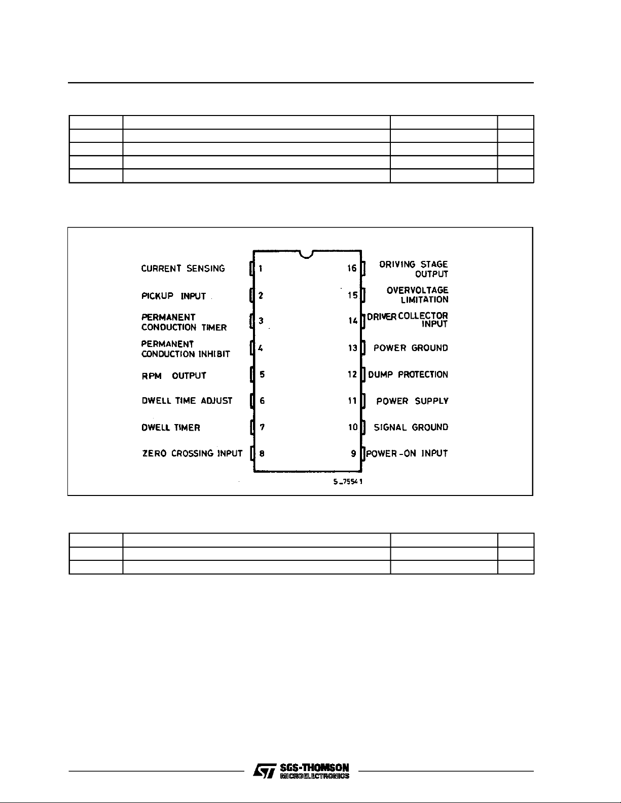
The L484 is an integratedcircuit designed for use
with an NPN darlington in breakerlessignition systemswithmagneticpickupsensorsand high energy ignitioncoils.
A keyfeatureofthe L484isflexibility.It canbeused
withawidevarietyof magneticsensorsthankstothe
BLOCK DIAGRAM
specialdesignwhichhastwoinputpinsfromthepickup ; the first is the zero crossing detector for the
ignitioncommandandthesecondpinisusedtocalculatethe dwelltime. Moreoveranotherpin is used
to adapt the L484 to variouspickup types.
Otherfeaturesof thedeviceincludedarlingtonovervoltageprotection,dump protection, a supply voltage rangeof 6-28 V.
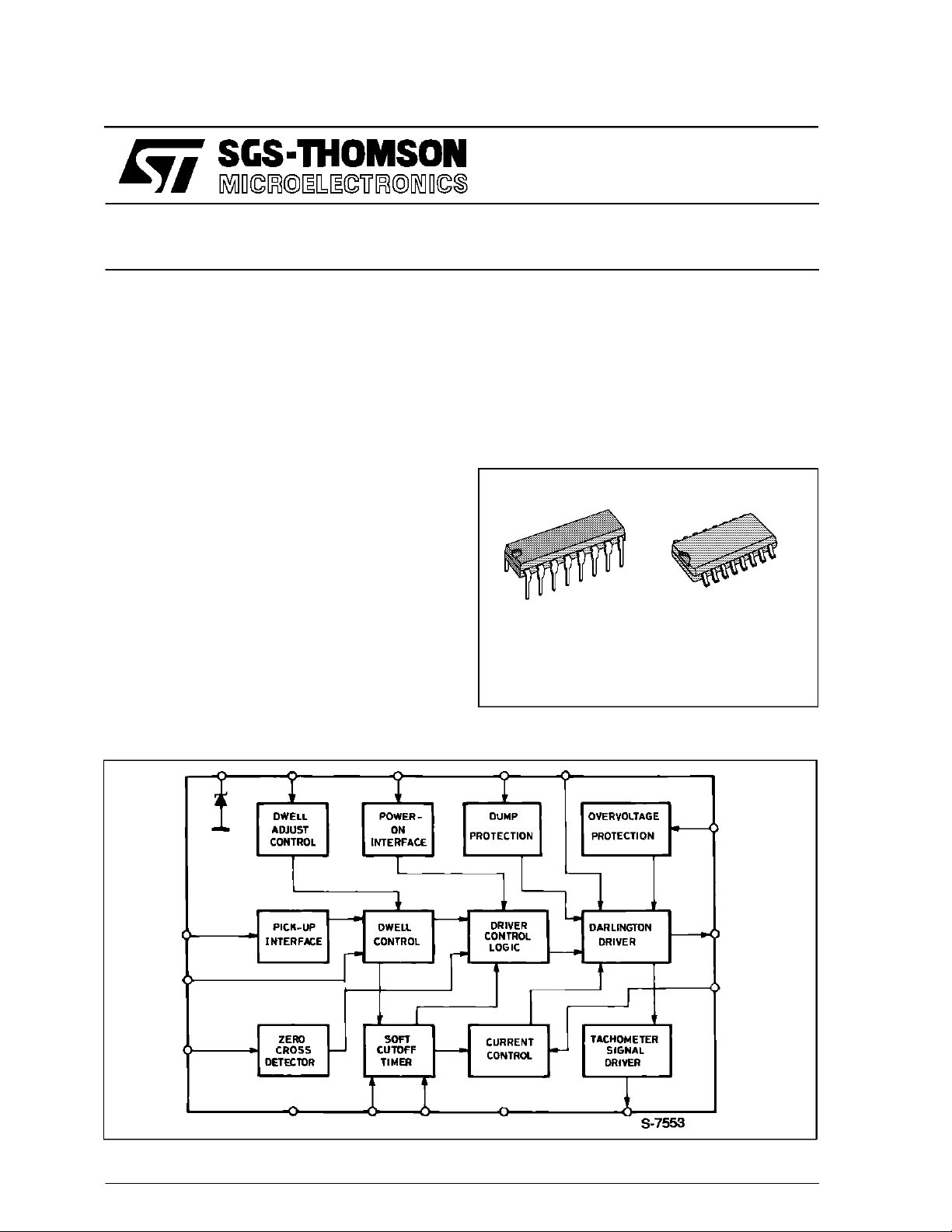
DIP16
ORDERING NUMBERS : L484 (DIP16)
L484D1 (SO16)
SO16
November 1991
1/11
Page 2
L484
ABSOLUTEMAXIMUM RATINGS
Symbol Parameter Value Unit
V
V
P
T
j,Tstg
PIN CONNECTION
Reverse Battery Voltage – 14 V
R
Dump Voltage 100 V
D
Power Dissipation at T
tot
=90°C 0.75 W
amb
Junction and Storage Temperature Range – 55 to 150 °C
THERMAL DATA
Symbol Parameter Value Unit
Thermal Resistance Junction-ambient (DIP16) Max 80 °C/W
Thermal Resistance Junction-alumina (SO16) Max 50 °C/W
2/11
R
th j-amb
R
th j-al
Page 3
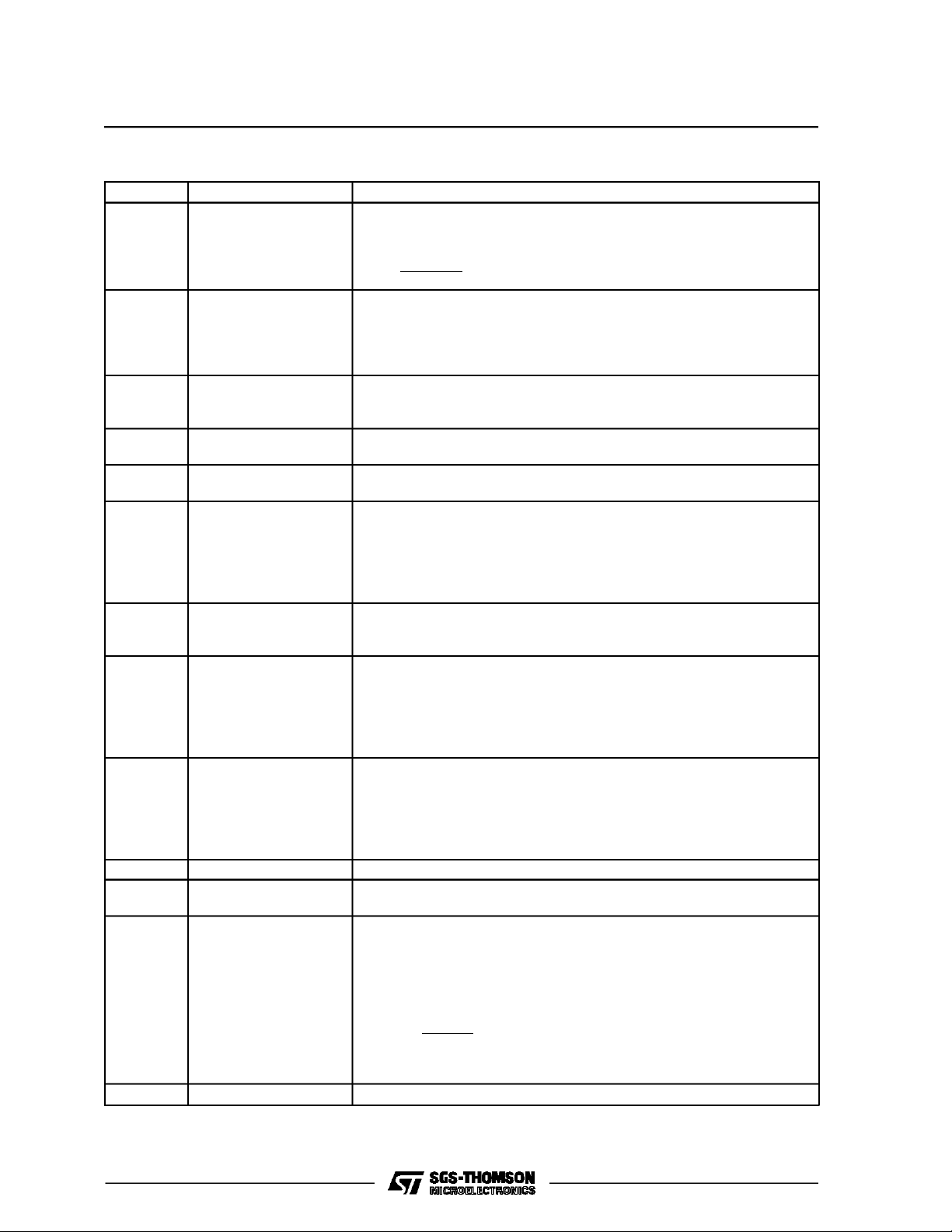
PINFUNCTIONS (refer to fig. 2)
N° Name Function
1 CURRENT SENSING
INPUT
2 PICKUP INPUT Magnetic Pickup Signal Input. This pin sets the dwell time, i.e. the max
3 PERMANENT
CONDUCT.
PROTECTION TIMER
4 PERMANENT CONDUCT.
PROTECTIONINHIBIT
5 RPM OUTPUT Open collector output signal which is at a low level when the final darlington
6 DWELL TIME ADJUST At high motor rotation speeds, i.e. when the peak value of the magnetic
7 DWELL CONTROL
TIMER
8 ZERO CROSSING
INPUT
9 POWER-ON INPUT A low level on this pin forces the external darlington into conduction
10 SIGNAL GROUND This pin must be connected to ground.
11 POWER SUPPLY Supply Voltage Input. A 7V (typ) zener is present at the input. The external
12 DUMP PROTECTION The device is protected against the load dump. In load dump condition an
Connection for Coil Current Limitation. The current is measured on the
sense resistor R
and divided on R1/R2. The current limitation value is
SENS
given by :
SENS
R
SENS
R2
R1 + R2
=
I
negative pickup voltage value starting from which the device can drive the
current into the coil. The real dwell time will be a function of the dwell
control logic. Increasing the resistor R11 the maximum conduction time
increases. The max input current foreseen is 2mA.
A capacitor C1 connected between this pin and ground sets the delay of the
permanent conduction protection in the coil current. Using a 50nF capacitor
the typical desaturation time delay for the protection is 75ms.
A low level on this input (max 0.7V) disables the protection, irrespective of
the state of pin 3. If the protection is used this pin must be left open.
is in ON status. The current is internally limited at 10mA.
pick-up signal exceedes 6V using R12 = 100KΩ, this pin may be used to
vary the dwell ratio. Adding a resistor in series R
between this pin and pin
a
11 the desaturation time is reduced. It is therefore possible to use this pin to
adapt the L484 to various pickup types. The maximum value of the resistor
is 200KΩ.
R
a
A capacitor C2 connected between this pin and ground sets the timing for
the dwell control. The recommended value is 100nF. The resistors R
provide an hysteresis to confirm ON state and avoid spurious sparks.
Zero cross detector input of the magnetic pickup signal for the ignition
actuation. At high motor rotation speeds, the external resistor R12 may be
used to vary the desaturation time ratio, to adapt the L484 to various
signal waveforms of time magnetic pick-up. Reducing the resistor value the
dwell time increases. Typically the range of values for resistor R12 is from
50KΩ to 150KΩ..
particularly useful in anti knock system. This function is particularly useful in
antiknock system because provides a spark time delay. Anyway the current
limitation, the permanent conduction protection and the dump protection
are operating even when pin 9 is at a low level. If this function is not used it
must be left open.
resistor R9 limits the current through the zener for higher supply voltages.
internal circuit, based on a zener diode and a darlington transistor,
switches off the external darlington and short circuits the supply.
By means of the external divider R8/R9 the protection threshold can be
changed and is given as first approximation by:
L484
b/Rc
Dth
R8+ R9
= 8.5
V
R9
+ 5 ⋅ 10
−4
R8
(the resistor R9 value must be higher than 4KΩ).
13 POWER GROUND This pin must be connected to ground.
* this function is particularly useful in antiknocksysteme because provides a spark time delay. anywaythe current limitation,the pemanent con
ductionprotection and the dump protectionare operating even when pin 9 is at a low level.
3/11
Page 4
L484
PINFUNCTIONS (continued)
N° Name Function
14 DRIVER COLLECTOR
INPUT
15 OVERVOLTAGE
LIMITATION
The collector current for the internal driver which drives the external
darlington is supplied through this pin. The external resistor R10 limits the
dissipation in the IC. The value this resistor depends on the darlington used
and on the limiting current in the coil.
The external darlington is protected against overvoltage by means of an
internal zener available at this pin. The external divider R5/R6 defines the
limitation value, typically given by :
30
+ 5 ⋅ 10
=
V
ovp
R5
−3
⋅
R6+ 30
16 DRIVING STAGE
OUTPUT
Current Driver for the External Darlington. To ensure stability on the current
limitation loop a capacitor C3 (typically 2.2nF, this value depending on the
darlington used) must be connected between this pin and the current
sensing input (pin 1).
ELECTRICAL CHARACTERISTICS (VS=14.4V ; TJ=- 40 to 125°C unlessotherwisespecified ; referred
to the test circuit)
Symbol Parameter Test Conditions Min. Typ. Max. Unit
V
V
V
V
SENS
V
V
I
I
I7D/I
I
I
TH
ZC
7C
7D
7C
7D
Operating Supply Voltage 6 28 V
S
Input Stage Voltage (pin 2 with
IS
160 200 240 mV
10KΩ resistor)
On Pick-up Thresh. Voltage at LOW RPM
VIS–30 VIS+30 mV
(pin 2)
Current Limitation Sensing Voltage (pin 1) VS= 6 to 16V 200 320 mV
Zero Crossing Thresh. Voltage (pin 8) 3 20 60 mV
Hysteresis Voltage (pin 8) 100 200 mV
H
C
D WELL
C
D WELL
Charge Current
Discharge Current
at LOW RPM
V
= 0.5V ;
pick-up
0.7
7
or pin 6 notconnected
7C
C
C
Charge Current
D WELL
Discharge Current
D WELL
(*) Note 1
at HIGH RPM
V
=9V
pick-up
7
8
13
30
15
33
44
3
µA
µA
µA
µA
4/11
I7D/I
V
V
V
V
pin3
I
3
V
Cp
CEsat
V
Z
OVZ
I
09
CH
I
CH
7C
Threshold Voltage
Output Current
Continuous Coil Current Protection Inhibit
(**) Note 2
T
=25°C
amb
(***) Note 3
0.7
0.85 4
0 0.7 V
LOW Voltage (pin 4).
Series Darlington Driver
Saturation Voltage (V
pin14 - 16
)
Zener Volt. Pin 11 I
External Darlington Overvoltage Protection
Zener Voltage
I
= 150mA
pin14
= 50mA
I
pin14
= 140mA 6.5 8.8 V
pin11
T
I
pin15
amb
=25°C;
= 5 to 15mA
25 35 V
0.4 1
Pin 9 Output Current in Low Status V9=0V 3 mA
Tachometer Signal Output LOW Voltage.
(pin5)
Output Leakage (pin 5)
ON Condition
= 0.5mA
I
sink
OFF Condition
=5V
V
pin5
3.2
3
0.6
0.7
10
V
µA
V
V
V
µA
Page 5

DUMPPROTECTION
Symbol Paramater Test Conditions Min. Typ. Max. Unit
V
DZ
(*)Note 1 : TD/T isgiven by the formula :
(**)Note 2 :
K value depends on thepick–up used in the application ; typically K = 0.1
(***)Note 3 : the permanent conduction protectionis guaranteed overthe full temperaturerange
Zener Dump (pin 12) I
TD 1
=
T 1 + I7D/I7C
TD K
=
T 1 + I7D/I7C
= 2mA 7.5 9.5 V
pin12
CIRCUI T OPERATI ON
The L484 controls the charging angle (dwell) and
thepeakvalueof theprimarycurrentin thecoilover
thefull range of operating conditions.
Thecoil current is limited to a predeterminedlevel
by meansof a negativefeedbackcircuit includinga
current sensing resistor, a comparator, the driver
stageand the power switch.
Thedwellcontrolcircuitkeepstheoutputstageinits
activeregionduring current limitation.The time the
outputstageis operatingin theactive region(desaturationtime), is sufficientto compensatefor possible variation in the energy stored due to the
accelerationof the motor ; moreoverthis time is limitedto avoid excessive power dissipation.
MAGNETICPICK–UPCHARACTERISTICS
Thetypical magneticpickupwaveformsare shown
in fig. 1,theamplitude of thesignalbeinga function
ofthe frequency.However on themarket thereare
manytypesof magneticpickup,of which the waveformsmay differ very much. Adjusting the valueof
theresistorR
onpin2 and/oraddingaresistor R
11
between the pin 6 (dwell adjust) and pin 11, as
shownintheapplicationcircuit,it ispossibletoadapt
theL484 toa widerangeof magneticpickupwaveforms.
Particularlyby means of the resistorR
onpin 2 it
11
is possibleto define the maximum advance of the
CONTROL OFTHE DWELLANGLE
The dwell angle control circuit defines the conduc-
tiontimeof the output darlington,versus thespeed
of rotation, the supply voltage and the characteristicsof thecoil.
In eachcyclethe timethetransistor operatesin the
activeregionis comparedwithareferencetimeand
the error signal amplifiedto advance or delay the
conductionin the next cycle.To limit the powerdissipation the desaturation time is typically fixed
to 10% of the periodT.
Atvery lowfrequenciestheON thersholdis fixedat
200mVofthe inputsignaland the desaturationtime
is mainly determined by the peak waveform. This
positivethresholdalsopreventspermanentconductionwhenthe motoris stopped.Whenthe inputfrequency increases the dwell control gradually sets
thedesaturationtimeto10%of theperiod.Athigher
frequenciesthe ON thresholdbecomesnegativeto
permitaconductionangleof morethan50%always
keepingdesaturationtime to 10%of the period.
a
CURRENT LIMITING
The currentin the coil is measured by means of a
voltagedropacrossa suitableresistorinthe emitter
lead of the power transistor. When the threshold
voltage(260mV typ) is reached,the coil current is
kept constantviaa feedbackloop.
conductionstart into the coil . Thisis veryuseful at
highpick–upfrequency.
L484
5/11
Page 6

L484
DARLINGTONOVERVOLTAGELIMITATION
The darlingtonis protected againstovervoltageby
meansofan externaldivider R
(pin15) andan
5/R6
internalzener.Thiszenerdrivestheexternaldarlingtonin order to limitthe collectorvoltage.
CHARGINGANGLESIGNAL OUTPUT
Thissignal is intended for tachometerapplications
(pin 5). It consists of an open collector stage with
current internallylimited at 10mA
PROTECTI O N CIRCUITS
PERMANENTCONDUCTIONPROTECTION
Thisfunctionisintendedto preventcontinuouscur-
rentconductioninthe finalstagewhenthemagnetic
pickupisopenorintermittent.Thedurationoftheinterventionis setby meansof a capacitor1 at pin 3.
Groundingpins 3 or 4, this protectionis eliminated.
The inhibit function at pin 4 is particularly useful
whenanexternallogiccontrolisused todisablethe
permanentconductionprotection.
REVERSEBATTERYAND DUMPPROTECTION
Dueto theexternalresistorsR
6,R7,R8,R10
thedevice is protectedagainst reverse battery. The load
dumpprotectionwithstandsupto100Vwithadecay
time ≤ 300ms. The intervention threshold for load
”POWERON” SIGNALINPUT
In the low statusthis input forces the externaldar-
lingtonintoconduction(pin9).Thiscontrolinputcan
be used togetherwith the conductiontime information coming from pin 5 to bypass the normal dwell
time calculation. When an external logic control is
usedto recognize particularengine condition (asin
antiKnock system).
dumpis fixed by means of an externaldivider connectedto pin 11.
OTHER APPLICATIONINFORMATION
If thesupplyis voltagedisconnected- or thebattery
wireis broken- whilethe currentis flowing through
the coil, theexternaldiodeD
keepsthe coilcurrent
1
fromrecirculatinginto the device: in this way both
deviceand darlingtonare protected.
ThezenerdiodeDz,connectedbetweenpin14and
GND,allowstowithstandpositivespikesupto200V.
Thedevice - usedin the recommended application
circuit - satisfies the ISO/DP 7637/1 overvoltage
standard.
Figure 1 : Typical Magnetic Pick–up Waveform and L484 Respon se at low and h igh
fequency.
6/11
Page 7

Figure 1 : TypicalMagneticPick-upWaveformand L484 Responseat Low and High Frequency
(continued).
L484
7/11
Page 8

L484
Figure 2 : Applic atio n Circuit.
8/11
Page 9

DIP16 PACKAGE MECHANICAL DATA
L484
DIM.
MIN. TYP. MAX. MIN. TYP. MAX.
a1 0.51 0.020
B 0.77 1.65 0.030 0.065
b 0.5 0.020
b1 0.25 0.010
D 20 0.787
E 8.5 0.335
e 2.54 0.100
e3 17.78 0.700
F 7.1 0.280
I 5.1 0.201
L 3.3 0.130
Z 1.27 0.050
mm inch
9/11
Page 10

L484
SO16 PACKAGE MECHANICAL DATA
DIM.
MIN. TYP. MAX. MIN. TYP. MAX.
A 1.75 0.069
a1 0.1 0.2 0.004 0.008
a2 1.6 0.063
b 0.35 0.46 0.014 0.018
b1 0.19 0.25 0.007 0.010
C 0.5 0.020
c1 45° (typ.)
D 9.8 10 0.386 0.394
E 5.8 6.2 0.228 0.244
e 1.27 0.050
e3 8.89 0.350
F 3.8 4.0 0.150 0.157
L 0.5 1.27 0.020 0.050
M 0.62 0.024
S8°(max.)
mm inch
10/11
Page 11

L484
Information furnished is believed to be accurate and reliable. However, SGS-THOMSON Microelectronics assumes no responsibility for
the consequences of use of such information nor for any infringement of patents or other rights of third parties which may result from its
use. No license is granted by implication or otherwise under any patent or patent rights of SGS-THOMSON Microelectronics. Specifications mentioned in this publication are subject to change without notice. This publication supersedes and replaces all information previously supplied. SGS-THOMSON Microelectronics products are not authorized for use as critical components in life support devices or
systems without express written approval of SGS-THOMSON Microelectronics.
1994 SGS-THOMSON Microelectronics - All Rights Reserved
Australia - Brazil - France - Germany - Hong Kong - Italy - Japan - Korea - Malaysia - Malta - Morocco - The Netherlands - Singapore-
SGS-THOMSON Microelectronics GROUP OF COMPANIES
Spain - Sweden - Switzerland - Taiwan - Thaliand - United Kingdom - U.S.A.
11/11
 Loading...