

Page 1
HALL–EFFECT PICKUP IGNITION CONTROLLER
.DIRECT DRIVING OF THE EXTERNAL PO-
WERDARLINGTON
.COILCURRENT CHARGING ANGLE(DWELL)
CONTROL
.COILCURRENT PEAK VALUELIMITATION
.CONTINUOUSCOILCURRENTPROTECTION
.CONDUCTION AND DESATURATION TIME
OUTPUT SIGNALS
.PERMANENT CONDUCTION PROTECTION
RESETOUTPUTSIGNAL
.OVERVOLTAGE PROTECTION FOR EXTER-
NALDARLINGTON
.LOADDUMP PROTECTION
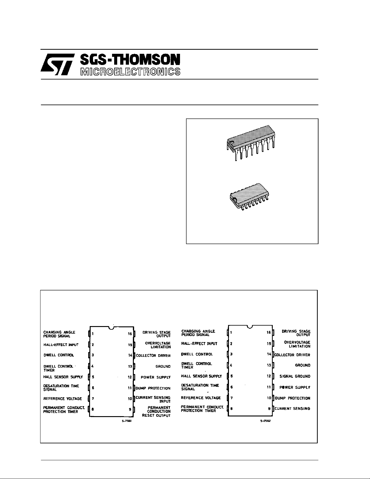
L482
DIP16
DESCRIP T IO N
The L482 is an integratedcircuit designed foruse
with an NPN darlington in breakerlessignition systemswithhall-effectpickupsensorsandhighenergy ignitioncoils.
It controls the energy stored in the ignition coil and
the desaturation time of the external darlingtonto
limit the power dissipation.
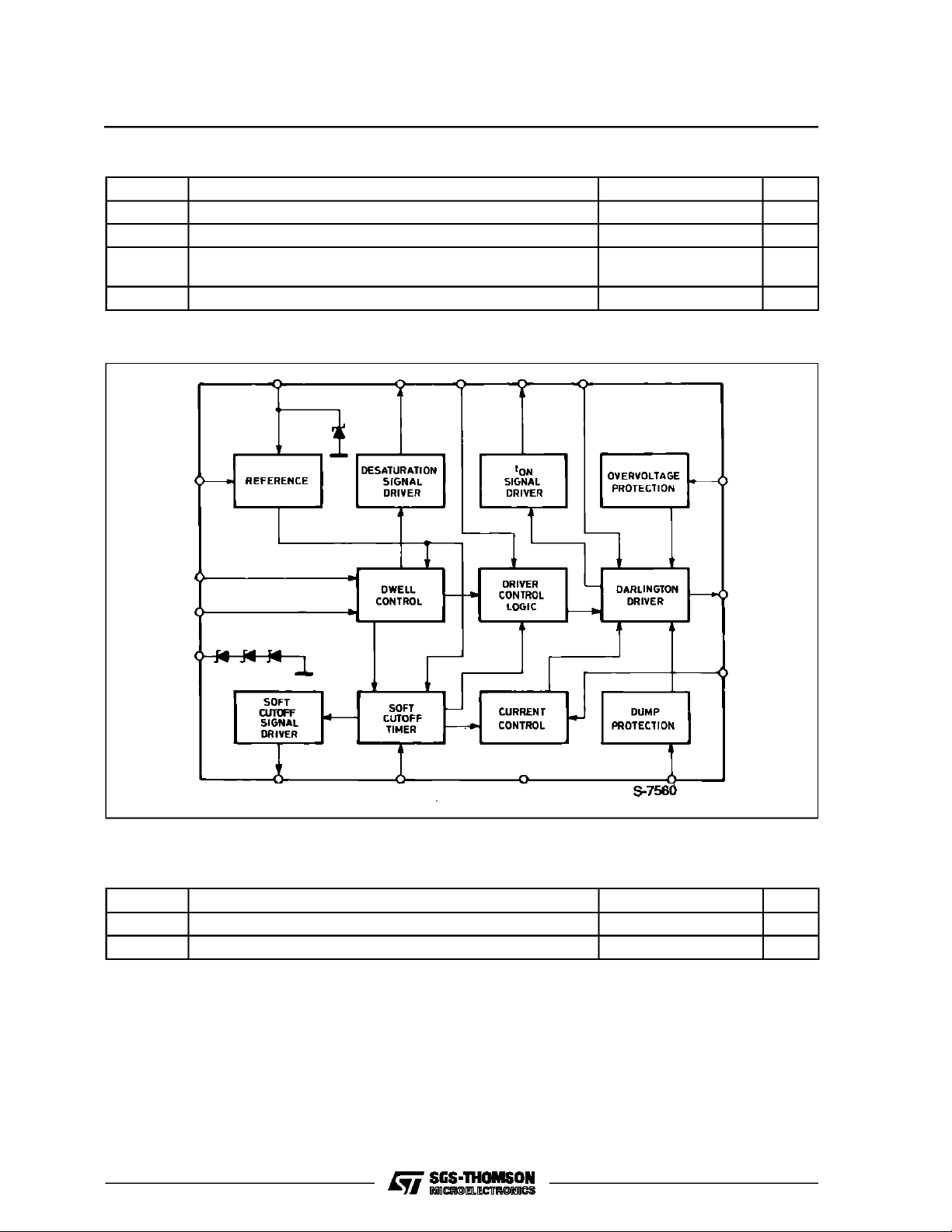
PI N CONNECTI ONS (top views)
DIP16
SO16
ORDERING NUMBERS : L482 (DIP16)
L482D1(SO16)
The L482isalsoparticularlysuitableforuseasignition controland driving stage in more sophisticated
car electronicsystems which employmicroprocessor cir cuits.
SO16
November 1991
1/11
Page 2
L482
ABSOLUTEMAXIMUM RATINGS
Symbol Parameter Value Unit
V
R
V
D
P
tot
T
j,Tstg
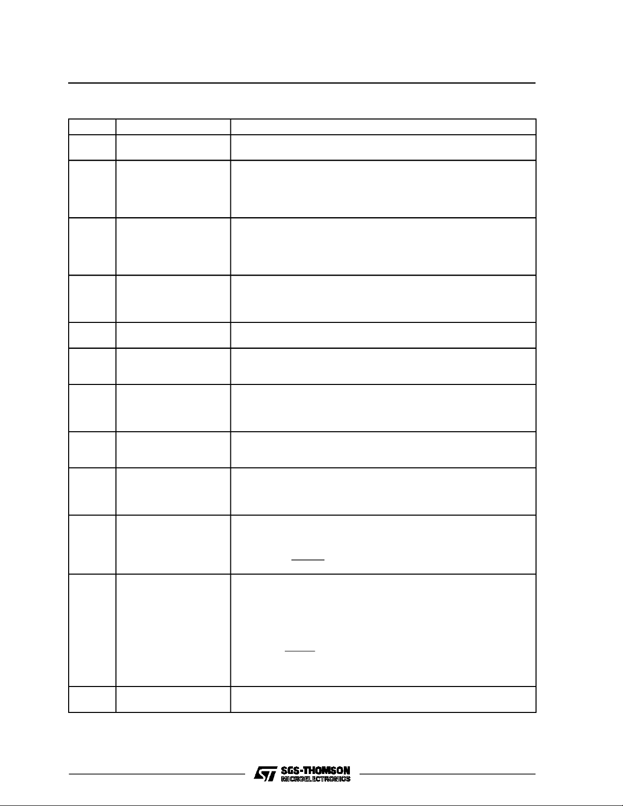
BLOCK DIAGRAM
Reverse Battery Voltage – 14 V
Dump Voltage 100 V
Power Dissipation at T
=90°C SO16
amb
DIP
1.2
0.65
Junction and Storage Temperature Range – 55 to 150 °C
W
W
THERMALDATA
Symbol Parameter Value Unit
R
th j-amb
R
th j-al
(*)Thermalresistance junction-aluminia with thedevice soldered onthe middle of an aluminiasupporting substrate measuring 15 x 20mm;
0.65mm thickness with infiniteheatsink.
2/11
Thermal Resistance Junction-ambient (DIP16) Max 90 °C/W
Thermal Resistance Junction-alumina (SO16) Max 50 °C/W
Page 3
PINFUNCTIONS (refer to fig. 3 for DIP16 package)
N° Name Function
1 CONDUCTION TIME
SIGNAL
2 HALL-EFFECT INPUT Hall-effect Pickup Input. A high level on this pin enables the current driving
3 DWELL CONTROL The average voltage on the capacitor C
4 DWELL CONTROL TIMER The capacitor C5 connected between this pin and ground is charged when
5 HALL SENSOR SUPPLY This pin can be used to project the Hall-effect pickup against the voltage
6 DESATURATION TIME
SIGNAL
7 REFERENCE VOLTAGE A resistor R11 connected between this pin and ground sets the internal
8 PERMANENT CONDUCT.
PROTECTION TIMER
9 PERMANENT CONDUCT.
RESET OUTPUT
(no available in
Micropackage) (*)
10 CURRENT SENSING
INPUT (*)
11 DUMP PROTECTION
(*)
A low level on this output signal indicates when the external darlington is in
the ON condition i.e. when the current flows through the coil (ton in fig.1)
into the coil. The effective coil charge will be a function of the dwell control
logic. A High to Low transition from the Hall-effect pickup is the signal for
ignition actuation. The input signal, supplied by the open collector output
stage of the Hall-effect sensor, has a duty cycle typically about 70%.
connected between this pin and
2
ground depends on the motor speed and the voltage supply. The
comparison between V
and VC5voltages determines the timing for the
C2
dwell control. The recommended value is 100nF using a 100KΩ resistor at
pin 7. For the optimized operation of the device, C2 = C5.
the Hall-effect output is high and is discharged at the High to Low transition
of the Hall-effect signal. The recommended value is 100nF using a 100KΩ
resistor at pin 7.
transients, The resistor R
limits the current into the internal zener.
a
Open Collector Output Signal. This output is high when the external
darlington is in desaturation condition (current limitation), see t
d
1.
current used to drive the external capacitors of the dwell control (C
) and permanent conduction protection (C1). The recommended value is
C
5
100KΩ.
A capacitor C1 connected between this pin and ground determines the
intervention delay of the permanent conduction protection, t
With a 1µF capacitor and 100KΩ resistorR
at pin 7 the typical delay is 1s.
11
of the figure 2.
pc
A low pulse on this output detects the intervention of the permanent
conduction protection, as shown in figure 2. Typically the duration of the
time t
is more than 100µs.
r
Connection for Coil Current Limitation. The current is measured on the
sense resistor R
and divided on R1/R2. The current limitation value is
S
given by :
I
SENS
= V
SENS
R1 + R2
⋅ R2
R
S
The device is protected against the load dump. In load dump condition an
internal circuit, based on a zener diode and a darlington transistor,
switches off the external darlington and short circuits the supply.
By means of the external divider R8/R9 the protection threshold can be
changed and is given as first approximation by:
L482
pulse in fig.
and
2
R8+ R
= 8.5 ⋅
V
Dth
9
R
9
+ 5 ⋅ 10
−4
⋅ R
8
(the resistor R9 value must be higher than 4KΩ).
12 POWER SUPPLY (*) Supply Voltage Input. A 7V (typ) zener is present at the input. The external
resistor R
limits the current through the Zener for high supply voltages.
7
3/11
Page 4
L482
PINFUNCTIONS (continued)
N° Name Function
13 GROUND This pin must be connected to ground.
14 DRIVER COLLECTOR The collector current for the internal driver which drives the external
15 OVERVOLTAGE
LIMITATION
darlington is supplied through this pin. The external resistor R
dissipation in the IC. The value of the resistor depends is a function of the
darlington used and on the limiting current in the coil.
The external is protected against overvoltage by means of an internal
zener available at this pin. The external divider R
defines the limitation
5/R6
value, given as first approximation by:
30
=
R
5
+ 5 ⋅ 10
V
ovp
−3
⋅ R6+ 30
10
limits the
16 DRIVING STAGE
OUTPUT
Current Driver for the External Darlington. To ensure stability and precision
of Tdesat C
and R3must be used. Recommended value for R3 is 2KΩ in
3
order not to change the open loop gain of the system.
may be added to C3to obtain greater flexibility in various application
R
C
situations.
and RC values ranges are 1 to 100nF and 5 to 30KΩ depending on the
C
3
external darlington type.
(*)These pins referonly tothe DIP package type.
For the SO16 version the permanent conduction reset output signal is not availableand the pin 9 becomes the current sensing input. Pin 10
replacesthe pin 11 function, pin 11 becomes thepower supply inputand pin 12 is usedas thesignal ground.
ELECTRICAL CHARACTERISTICS (VS=14V, –40°C≤Tj≤125°C referred to application circuit of
figure 3 regarding DIP-16 package version)
Symbol Parameter Test Conditions Min. Typ. Max. Unit
V
S
I
S
V
Z
V
I
I
I
V
Hz
I
HZ
V
CE sat
(V14–V16)
V
SENS
I
3D
I
3C
I3C/I
3D
V
OVZ
V
7
t
d
Operating Supply Voltage 6 28 V
Supply Current V12= 4.5V 25 mA
Zener Voltage (pin 12) IZ= 80mA 6.5 8.8 V
Sensor Input (pin 2)
LOW Voltage
HIGH 2.5
Sensor Input Current (pin 2) VI= LOW
= 6 to 16V
V
S
Hall-cell Supply Zener Voltage
IHz= 10mA 19 22 25 V
–12 –1 mA
0.5 V
V
(pin5)
Hall-cell Supply Zener Current
(pin5)
Series Darlington Driver Sat.
Voltage
Current Limit. Sensing Voltage
t = 10ms
=25°C
T
AMB
I
= 70mA
o
= 150mA 0.4
I
o
VS= 6 to 16V 200 400 mV
100 mA
0.6
1.0
V
V
(pin10)
C2 Discharge Current
C2 Charge Current
External Darlington Overvoltage
Protection Zener Voltage
VS= 6 to 16V
(*) Note 1
I
= 5mA to 15mA
OVZ
=25°C
T
AMB
0.2
5
6
3.4
20
35
25 30 35 V
µA
µA
Reference Voltage 2.5 3.5 V
Desaturation Time f = 40Hz VS= 14V 0.6 1.2 1.57 ms
4/11
Page 5

ELECTRICAL CHARACTERISTICS (Continued)
Symbol Parameter Test Conditions Min. Typ. Max. Unit
t
PC
V
1
V
6
I
6L
I
9L
Permanent Conduction
Protection Time (pin 8) (see fig.
2)
Charging Angle Output Voltage
LOW
HIGH
Desat. Time Output Low
Voltage
Desat. Time Leakage Current
(pin6)
Permanent Conduction Reset
Leakage Current (pin9)
VI=H
=1µF
C
I
=0
I
SINK
I
= 1mA
SINK
I
I
I
= 1.5mA
SOURCE
= 2.5mA
SOURCE
= 0.5mA 0.7 V
6 (sink)
V6= 5V 10.5 µA
V9= 5V 10.5 µA
135s
0.5
1.2
3
5
L482
V
V
V
V
APP LICATION INFO RMATION
Figure 1 : Main Wa v ef o rms.
5/11
Page 6

L482
Figure 2 : Low Frequency Condition an d Permanent Conduction Protection.
Figure 3 : Application circuit (DIP–16).
6/11
Page 7

Figure 4 : App lic a tion Circuit (SO –16 ).
L482
CIRCUIT OP ERA TI ON
TheL482controltheconductiontime(dwell)andthe
peakvalueof theprimarycurrentin thecoiloverthe
full rangeof operatingconditions.
The coil current is limited to a predeterminedlevel
by meansof a negativefeedbackcircuitincludinga
current sensing resistor, a comparator, the driver
stageand the powerswitch.
The dwell controlcircuit maintainstheoutputstage
in itsactiveregionduringcurrentlimitation.Thetime
the outputstageisintheactiveregion(desaturation
time) is sufficient to compensatefor possiblevariationsin the nergy storeddue to the accelerationof
the motor; moreoverthistimeislimitedtoavoidexcessivepower dissipation.
CONTROL OF THE DWELLANGLE (fig.1 and 4)
The dwell angle control circuit calculates the con-
ductiontime Dfor the outputtransistorin relation to
the speedof rotation,to the supply voltageand to
the characteristicof thecoil.
On the negativeedgeof the Hall-effect inputsignal
the capacitorC
currentI
3D
beginsdischargingwitha constant
2
. When theset peakvalue of thecoilcurrent is reached,this capacitorcharges with a constant current I
=13.3 x I3Dand the coil current is
3C
kept constantby desaturatingthe driverstage and
the externaldarlington.
The capacitor C
starts charging on the positive
5
edgeof the Hall-effect input signal with a constant
currentI
4C
.
Thedwellangle,andconsequentlythestartingpoint
ofthecoilcurrentproduction,isdecidedby thecomparisonbetweenV
andVC5. A positivehysteresis
C2
isaddedto the dwell comparatorto avoid spurious
effectsand C
israpidlydischargedon the negative
5
edgeof Hall-effectsinput signal.
In this way the averagevoltage on C
increases if
2
the motorspeed decreasesand viceversain order
to maintainconstanttheratiotdatany motorspeed.
T
td is kept constant (andnot d = cost) to control the
power dissipation and to have sufficient time to
avoidlow energy sparksduring acceleration.
The chargingtime D – td dependson the coil and
the voltagesupply.
DESATURATION TIMES IN STATIC CONDITIONS.Instaticconditions,if C
2=C5
asrecommendedand if the valuesof the applicationcircuitof fig.
3, 4 are used.
td 1
=
T1+I
3C/I3D
7/11
Page 8

L482
DESATURATIONTIMESINLOWANDHIGHFREQUENCYOPERATION.Duetotheupperlimitofthe
voltagerangeof pin3,if thecomponentsof fig.3, 4
areused, below10Hz(300RPMfor a4 cylinder engine) the OFF time reaches its maximum value
(about50ms)andthenthecircuitgraduallylosesthe
controlof the dwellangle becauseD = T – 50ms
Over200Hz (6000RPMfora 4 cylinderengine)the
availabletimefortheconductionislessthan3.5ms.
If theused coil is6mH, 6A,the OFFtime isreduced
to zero andthe circuitlosesthe dwellanglecontrol.
TRANSIENT RESPONSE. The ignition system
must deliverconstant energy even during the conditionof accelerationand decelerationof the motor
below 80Hz/s. These conditions can be simulated
by means of a signal generator with a linearly modulated frequency between 1Hz and 200Hz (this
correspondstoachangebetween30and6000RPM
for a 4 cylindersengine.
CURRENT LIMIT.The currentin thecoil is monitored by measuring the I
sensingresistorR
lington.I
WhenthevoltagedropacrossRsreachesthe internalcomparatorthresholdvaluethefeedbackloopis
activatedand I
externaldarlingtonin theactive region. In this condition:
WhenaprecisepeakcoilcurrentisrequiredR5must
be trimmedor an auxiliaryresistor divider (R
added :
Icpeak(A) = ( + 1)
sense
ontheemitteroftheexternaldar-
s
is givenby :
I
sense=Icoil+I16
keptconstant(fig. 1)forcingthe
sense
I
sense=Icoil
V
SENS
R
S
current flowing in the
sense
R
1
R
2
1,R2
DARLINGTONOVERVOLTAGELIMITATION
The darlingtonis protectedagainst overvoltageby
meansof an externaldividerR
internalzener.Thiszenerdrives theexternaldarlingtonin orderto limit the collectorvoltage.
REVERSEBATTERY PRTOTECTION. Due to the
presenceof externalimpedanceatpin5, 10,11,14,
15, L482 is protectedagainstreverse battery voltage.
DUMPPROTECTION.
The load dump protection withstands up to 100V
with a decaytime ≤ 300ms. The interventionthresholdforloaddumpisfixedbymeansof anexternal
divider connected to pin 11 (DIP-16 package version)or to pin 10 using a Micropackagetype.
NEGATIVESPIKEPROTECTION.If correctoperationis requestedalso duringshort negativespikes,
thediode DS and capacitorC
USEOF THE IC ELECTRONICADVANCE SYSTEM
When the device is digitally controlled the control
unit transmits a suitable input signal to the power
module, receivingin turninformationthat allowsthe
controlof thedwell and theontime of thefinaltransistor.
ForthisreasonL482providesthefollowingoutputs:
(pin15) and an
5/R6
mustbe used.
s
.a time signal equal to the time in which the final
)
Darlingtonis intheactiveregioni.e.whenthecoil
current islimited (V
signalmust be TTL compatible.
) as shown in figure1.This
ds
PROT ECT IO N CIRCUIT
PERMANENTCONDUCTION PROTECTION
The batteryvoltageis applied to ignitionmoduleby
meansof theignitionkey. In these conditions, with
the motor stopped, it is necessarythat there is no
permanentconductionin the ignitioncoil irrespective of the polarity of the input signal.
The L482incorporatesa timing circuitto implement
thisprotection; thedurationoftheinterventionisset
by means of a capacitor C
=100kΩ, whenthe inputsignalis highfor more
R
11
than1 s, the coilcurrent graduallydecreasesdown
to zero to avoid spurious sparks (seefig. 2).
This timing allows normal operation of the module
above30RPM.
8/11
at pin 8 = 1µF, and
1
.a TTL compatibleoutput from the timing circuit
in figure2). Thispulse,availableonly using
(V
rs
the DIP-16packageversion is present after the
protectionagainstcranking transients.
.a time signal equal to the time in which the final
Darlington,is in”on” condition(V
current flows throughthe coil, see fig. 1.
OTHER APPLICATIONINFORMATION
Ifthe supplyvoltageisdisconnected- or thebattery
wireis broken- whilethe current is flowing through
thecoil,the externaldiodeD
fromrecirculating into the device : in this way both
deviceanddarlington are protected.
keepsthe coilcurrent
1
)i.e.whenthe
on
Page 9

DIP16 PACKAGE MECHANICAL DATA
L482
DIM.
MIN. TYP. MAX. MIN. TYP. MAX.
a1 0.51 0.020
B 0.77 1.65 0.030 0.065
b 0.5 0.020
b1 0.25 0.010
D 20 0.787
E 8.5 0.335
e 2.54 0.100
e3 17.78 0.700
F 7.1 0.280
I 5.1 0.201
L 3.3 0.130
Z 1.27 0.050
mm inch
9/11
Page 10

L482
SO16 PACKAGE MECHANICAL DATA
DIM.
MIN. TYP. MAX. MIN. TYP. MAX.
A 1.75 0.069
a1 0.1 0.2 0.004 0.008
a2 1.6 0.063
b 0.35 0.46 0.014 0.018
b1 0.19 0.25 0.007 0.010
C 0.5 0.020
c1 45° (typ.)
D 9.8 10 0.386 0.394
E 5.8 6.2 0.228 0.244
e 1.27 0.050
e3 8.89 0.350
F 3.8 4.0 0.150 0.157
L 0.5 1.27 0.020 0.050
M 0.62 0.024
S8°(max.)
mm inch
10/11
Page 11

L482
Information furnished is believed to be accurate and reliable. However, SGS-THOMSON Microelectronics assumes no responsibility for
the consequences of use of such information nor for any infringement of patents or other rights of third parties which may result from its
use. No license is granted by implication or otherwise under any patent or patent rights of SGS-THOMSON Microelectronics. Specifications mentioned in this publication are subject to change without notice. This publication supersedes and replaces all information previously supplied. SGS-THOMSON Microelectronics products are not authorized for use as critical components in life support devices or
systems without express written approval of SGS-THOMSON Microelectronics.
1994 SGS-THOMSON Microelectronics - All Rights Reserved
Australia - Brazil - France - Germany - Hong Kong - Italy - Japan - Korea - Malaysia - Malta - Morocco - The Netherlands - Singapore-
SGS-THOMSON Microelectronics GROUP OF COMPANIES
Spain - Sweden - Switzerland - Taiwan - Thaliand - United Kingdom - U.S.A.
11/11
 Loading...