

Page 1
DRIVESDIRECTLY300 mAALARMLOAD
.
PROGRAMMABLEINPUTPOLARITYTO
.
ACTIVATETHEOUTPUT STAGE
PROGRAMMABLEDELAYTIME
.
PROGRAMMABLEOUTPUTDUTY CYCLE
.
OUTPUTSHORTCIRCUITPROTECTION
.
OVERVOLTAGEANDTHERMAL
.
PROTECTION
L4620
LIQUIDLEVEL ALARM
Minidip
DESCRIPTION
The L4620is anintegratedcircuit,designedforthe
liquid level control in automotiveapplications. The
liquid level is indicated by an attenuationbetween
transmittedand receivedsignalacrossa sensortip
in thelquid. If the attenuationexceedesan internal
threshold- sensortipoutsidetheliquidorliquidtemperaturehigherthana determinedvalue- asquarewave alarm output indicates an unsufficient liquid
condition.Iftheliquidlevelisrestoredbeforetheend
of a delaytime the alarmis notactivated.
Throughtwopinsitis possibletoprogram:thedelay
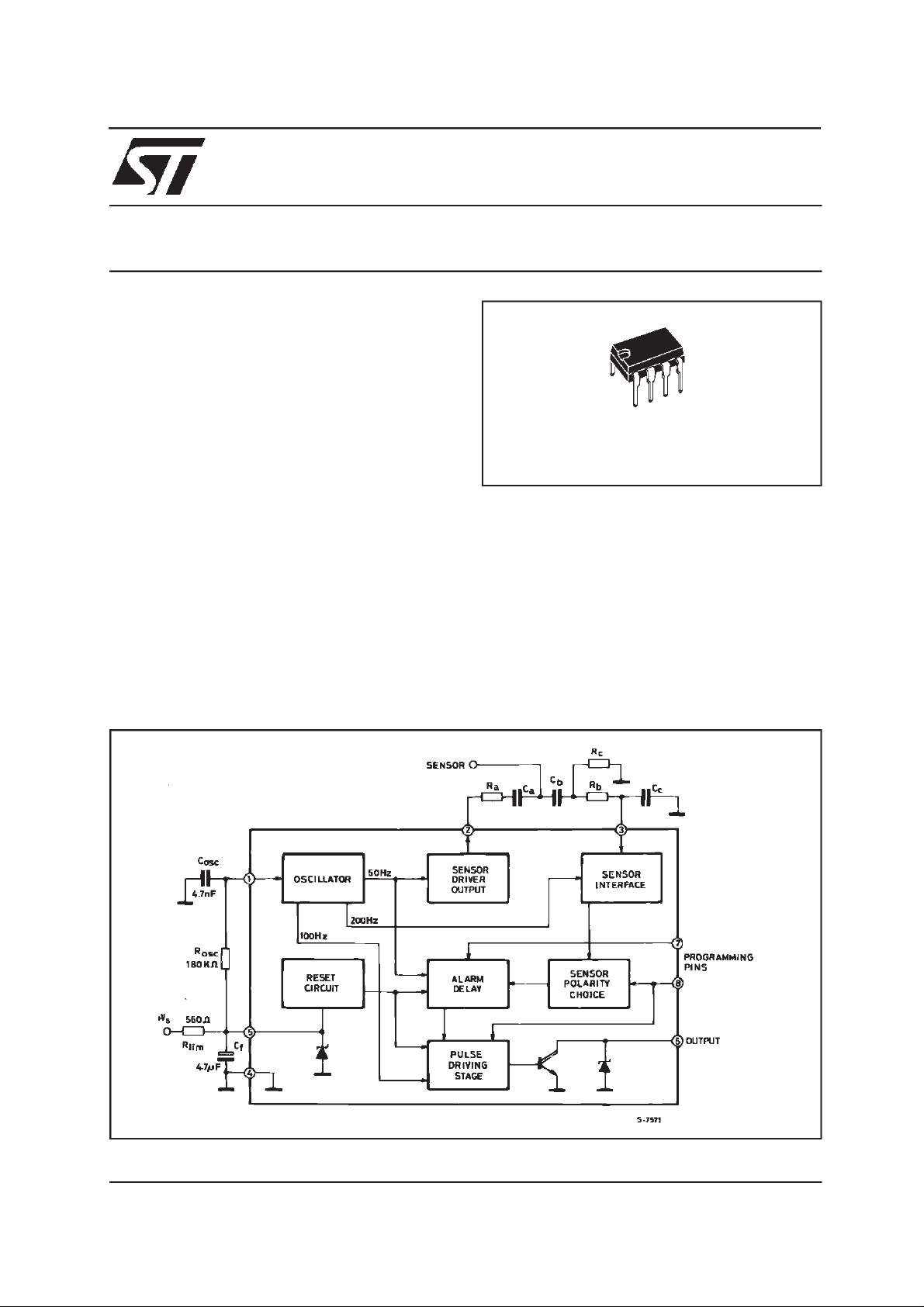
BLOCK DIAGRAM
ORDERING NUMBER : L4620
time to activate thealarm, the duty cycleof the
output squarewave,the polarity ofthe input thresholdof thesensorfor alarmactivation.
TheabovefeaturesmaketheL4620particularlyversatilefor many applicationsand givethe possibility
tousevarioussensor types.
Internal circuits prevent spurious indications from
the liquid sensor and a latch keeps the alarmactivateduntilthesupplyvoltageisswitchedoff.Thedeviceincludesthermalshutdownprotections.
December 1999
1/9
Page 2
L4620
ABSOLUTE MAXIMUM RATINGS
Symbol Parameter Value Unit
I
V
I
out
P
T
j,Tstg
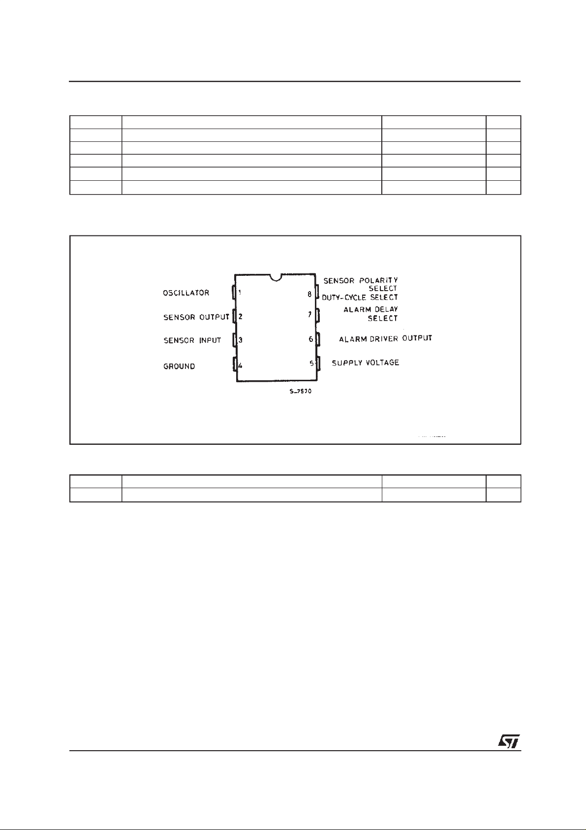
PI N CONNE CTION (top view)
Supply Current (VS>VZ) 200 mA
S
Sensor Input Voltage (V2High) 7 V
3
Output Current 500 mA
Power Dissipation at T
tot
amb
=70°C
0.8 W
Junction and Storage Temperature Range – 55 to 150
°C
THERMAL DATA
Symbol Parameter Value Unit
Thermal Resistance Junction-ambient Max 100 °
2/9
R
th j-amb
C/W
Page 3

PIN FUNCTION (BlockDiagram)
L4620
N
°
1 Oscillator A capacitor C
Name Function
connected to ground and a resistor R
osc
voltage) set the frequency of the internal oscillator. The period is given by: T
+ 5000) C
(R
osc
osc
connected to pin 5 (supply
osc
osc
= 0.693
2 Sensor Output A squarewave is available at this pin to drive the external sensor. The output
frequency is 1/32 of the internal oscillator fosc, i.e. 50Hz using the values of
= 180kΩand C
R
osc
= 4.7nF for the external components.
osc
3 Sensor Input Connection for liquid level sensing. During the zero level of the squarewave signal at
pin 2, the internal sensing circuit is disabled. During the high level of the wave shape
the input is compared with a threshold which depends on the output sensor volta
= 0.4V2(typ). If the input voltage becomes higher than the above V
V
SENSH
value is reduced to V
V
sens
= 0.22V2(typ), providing an hysteresis available with
SENSL
SENSH
, the
both the programmable polarities.
4 GND This pin must be connected to ground.
5 Supply Voltage Supply voltage input. A 4.5V (typical) zener is present at the input. The external
resistor limits the current through the zener for high supply voltages. Moreover when
the voltage at this pin is down 2.5V (typical) the internal reset circuit is activated
6 Alarm Driver
Output
7 Alarm Delay
Select
An internal open collector stage is available at this pin to drive the external alarm
indicator by a rectangular waveshape. The output period depends on the external
component R
osc
and C
. Using the recommended values of block diagram th
osc
This program pin selects the alarm delay to activate the output stage after a low liquid
level indication of the sensor. The delay depends on the internal oscillator frequency.
Refer to application circuit, if this pin is kept low the typical delay is 10.
8 Sensor Polarity
Select Output
Duty-cycle
Select
Through this pin it is possible to program both the sensor polarity with respect to the
internal threshold and the duty-cycle of the output waveform which drives the alarm.
When this pin is kept low the output rectangular wave duty cycle is 1:64
(T = 320ms, t = 5ms in fig. 2) and the output is activated, after the delay time, if the
voltage at pin 3 is higher than V
. When the voltage at this pin is high the output
SENS
duty cycle is 50% (t = 160ms) and the output goes on, after the delay
3/9
Page 4

L4620
ELECTRICAL CHARACTERISTICS (T
=25°C, unless otherwise specified. Refer to block diagram
amb
for externalcomponent values)
Symbol Parameter Test Conditions Min. Typ. Max. Unit
V
I
f
osc
V
7,V8
I
7,I8
V
I
V
SENSH/V2
V
sens
_____
V
V
clamp3L
V
clamp3H
I
sens
Internal Zener Voltage (pin 5) IS= 24 mA 4 4.5 5 V
Z
Supply Current (pin 5) VS= 3.8 V 6.5 11 mA
S
Oscillator Frequency (pin 1)
Programming Pins Input
Voltage (pin 7, 8)
Programming Pins Input Current
(pin 7, 8)
Sensor Drive Output Voltage, (*) V2= Low,
2
Sensor Driver Output Current – 1 1 mA
2
Sensor Input High Threshold
Voltage Versus V
(pin 3)
2
Sensor Input Low Threshold
Voltage Versus V
2
(pin 3)
2
Sensor Input Clamping Voltage
(pin 3)
= 180 kΩ,C
R
osc
osc
= 4.7 nF
Low State 0.3 V
High state 2 V
V7=V8=0V –1
V
7=V8=VZ
=1mA
I
2
= High,
V
2
=1mA
I
2
V
= High
2
V
pin 3<VSENSL
V
= High
2
V
pin 3>VSENSH
– 100µA<I
= Low
V
2
sens
< 100µA
V2= High
= – 100 µA
I
3
I
= + 100µA
3
Sensor Input Bias Current (pin3)V
= High 1.2
sens
1.45 1.6 1.75 kHz
V
–1 VZ–0.4 V
Z
0.33 0.4 0.47
0.15 0.22 0.29
– 0.1 0.1 V
– 0.8 – 0.6 – 0.4 V
V
Z
150
0.4 V
VZ+0.8 V
µA
µA
µA
10.24 sec
V
out(sat)
T
Delay Time f
d
Output Stage Saturation
= 1.6 kHz
osc
= Low
V
7
V
= High 20.48 sec
7
I
= 200 mA 1.3 V
out
Voltage (pin 6) (**)
V
out(clamp)
Output Stage Overvoltage
I
=70mA 19 21 23 V
out
Protection (pin 6)
I
LEAK
*) This is a squarewave signal.The frequencyis given by : f = f
**) The output squarewave signal frequency is given by f = fosc.
The duty cycle depends on the state of the pin 8 and can be or 1 : 2 or 1 : 64, i.e. refer to figure 2, T = 320 ms, t = 160 or 5 ms when
the oscillator frequency f
Leak Current (pin 6) P6 = 15V; P7 = P8 = GND 100 µ
= 1.6 KHz.
osc
512
1
32
1
osc
.
A
4/9
Page 5

CIRCUI T OPERAT ION
L4620
TheL4620liquid levelalarm isdesignedto operate
witha varietyof sensortypeswhichchangeimpedancedependingon whetherthesensoris aboveor
belowthelevelofaliquid.Iftheimpedancevariation
of ther liquid itselfis sensed,a very simple sensor
(two electrodes) can be used. The output stage
drivesdirectlythealarmindicatorwitha 300mArectangularwavesignal,thedutycycleofwhichisprogrammable.
SENSORINTERFACE.
Asshownintheapplicationcircuit,thesensoriscon-
nectedso thatit variesthe attenuationofa squarewavesignalbetweenpin 2and pin3 whereitspositivehalfcycleiscomparedwiththereferencethreshold(withhysteresis).
Thisfrequency,generatedinternallyby a 50%duty
cycle oscillator, is 50Hz in the typical application
(R
osc
= 180KΩ C
=4.7nF).
osc
Thethresholdofthesensorinputis afunctionofthe
outputvoltageatpin2.Thehysteresisisprovidedby
a Schmitttriggercomparator.As shownin figure1,
this gives hysteresis with either threshold polarity
selected.
TheACdrivingof thelevel sensorallowsthe useof
a capacitive filter (C
A,CB,CC
in block diagram)
which acts as a bandpass filter at the frequency
used.TheresistorR
intheapplicationcircuitbiases
C
the sensorinputstage. In this waytheinterference
problemstypicalof automotiveapplicationsare reducedconsiderably.If,however,itis not necessary
to decoupleand filter the sensor a simple resistive
networkmaybe used,eliminatingthecapacitors.
SPURIOUSINDICATION PROTECTION.
Topreventspuriousalarmsignalswhentheliquidis
agitatedor in the presence of interference,the deviceincludestwo protectionmechanism:
Firstly,thesensorinterfacewhichsamplesthepositivehalfcycleofthesensorsignalactivatesitsoutput
onlyiftherearefourconsecutivealarmconditionindications.Secondly,the alarm outputstage is only
activated after an externally programmable delay.
During this delay if the alarm conditionceases the
alarmoutputwill not be activated.
Usingthe values C
= 4.7nF and R
osc
= 180KΩ,
osc
whichgive a typicaloscillatorfrequencyof1.6KHz,
delaysofabout10s (programmingpin7 low)or20s.
INTERNALMEMORY.
Whenthealarm outputhasbeenactivatedaninter-
nal latch holds it in the active state until the power
supply is removed. This feature ensures that the
alarmwillnotbeinterruptedifthesensorconnection
breaks.
OUTPUTSTAGE.
Throughpin8 itispossibleto programthedutycycle
of the alarmsignal waveform(see figure2). When
pin8ishightheoutputsignalhasa dutycycleof50%
; ifpin 8 is low thedutycycle is 1 : 64.The periodof
theoutputsignalisalways320msusingthecomponentvaluesindicatedin block diagram.
Theoutputstagecandeliverupto300mAandisprotectedinternallyagainstovervoltages(bya zener).
A thermalshutdowncircuit providesadditionalprotection.
5/9
Page 6

L4620
SENSOR INPUT WAVEFORM
Figure1a : Pin8 Low; Alarmwith InputVoltage> Threshold.
Figure1b : Pin8 High; AlarmwithInput Voltage< Threshold.
6/9
Page 7

L4620
Figure2a : OutputAlarm Waveformwith Pin8 High:t = T.
1
2
1
Figure2b : OutputAlarmWaveformwithPin 8 Low: t = T.
64
7/9
Page 8

L4620
DIM.
MIN. TYP. MAX. MIN. TYP. MAX.
A 3.32 0.131
a1 0.51 0.020
B 1.15 1.65 0.045 0.065
b 0.356 0.55 0.014 0.022
b1 0.204 0.304 0.008 0.012
D 10.92 0.430
E 7.95 9.75 0.313 0.384
e 2.54 0.100
e3 7.62 0.300
e4 7.62 0.300
F 6.6 0.260
I 5.08 0.200
L 3.18 3.81 0.125 0.150
Z 1.52 0.060
mm inch
OUTLINE AND
MECHANICAL DATA
Minidip
8/9
Page 9

L4620
Information furnished is believed to be accurate and reliable. However, STMicroelectronics assumes no responsibility for the consequences of use of such information nor for any infringement of patents or other rights of third parties which may result from its use. No
license is granted by implication or otherwise under any patent or patent rights of STMicroelectronics. Specification mentioned in this
publication are subject to change without notice. This publication supersedes and replaces all information previously supplied. STMicroelectronics products are not authorized for use as critical components in life support devices or systems without express written
approval of STMicroelectronics.
The ST logo is a registered trademark of STMicroelectronics
1999 STMicroelectronics – Printed in Italy – All Rights Reserved
STMicroelectronics GROUP OF COMPANIES
Australia - Brazil - China - Finland - France - Germany - Hong Kong - India - Italy - Japan - Malaysia - Malta - Morocco -
Singapore - Spain - Sweden - Switzerland - United Kingdom - U.S.A.
http://www.st.com
9/9
 Loading...