

Page 1
查询L3235N 供应商
L3234
®
HIGHLY INTEGRATED SLIC KIT TARGETED TO PABX
AND KEY SYSTEM APPLICATIONS
HIGHLY INTEGRATED SUBSCRIBER LINE
INTERFACE KIT FOR PABX AND KEY SYSTEM APPLICATIONS
IMPLE MENTS AL L KEY ELEMEN TS OF T HE
BORSCHT FUNCTION
INTEGRATED ZERO CROSSING BA LANCED
RINGING INJECTION ELIMINATES EXTERNAL RELAY AND CENTRALISED RINGING
GENERATOR
ZERO NOISE INJECTED ON ADJACENT
LINES DURING RINGING SEQUENCE
LOW POWER IN STANDBY AND ACTIVE
MODES
BATTERY FEED WITH PROGRAMMABLE
LIMITING CURRENT
PARALLEL LATCHED DIGITAL INTERFACE
SIGNALLING FUNCTIONS (OFF HOOK,
GND-KEY)
LOW NUMBER OF EXTERNAL COMPO-
NENTS
INTEGRATED THERMAL PROTECTI ON
INTEGRATED OVER CURRENT PROTEC-
TION
0°C TO 70°C: L3234/L3235N
-40°C TO 85°C: L3234T/L3235NT
DESCRIPTION
The L3234/L3235N is a highly integrated SLIC
KIT targeted to PABX and key system applications
The kit integrates the majority of functions required to interface a telephone line. The
L3234/L3235N implements the main features of
the broths function:
- Battery Feed (Balanced Mode)
- Ringing Injection
- Signalling Detection
- Hybrid Function
L3235N
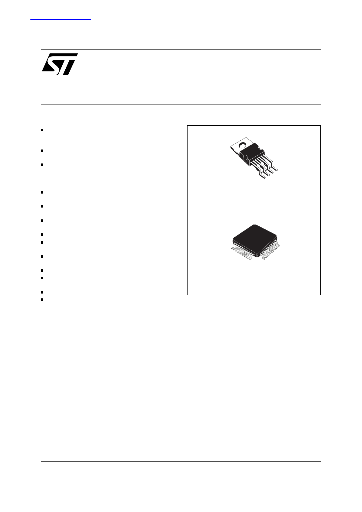
HEPTAWATT
ORDERING NUMBER:
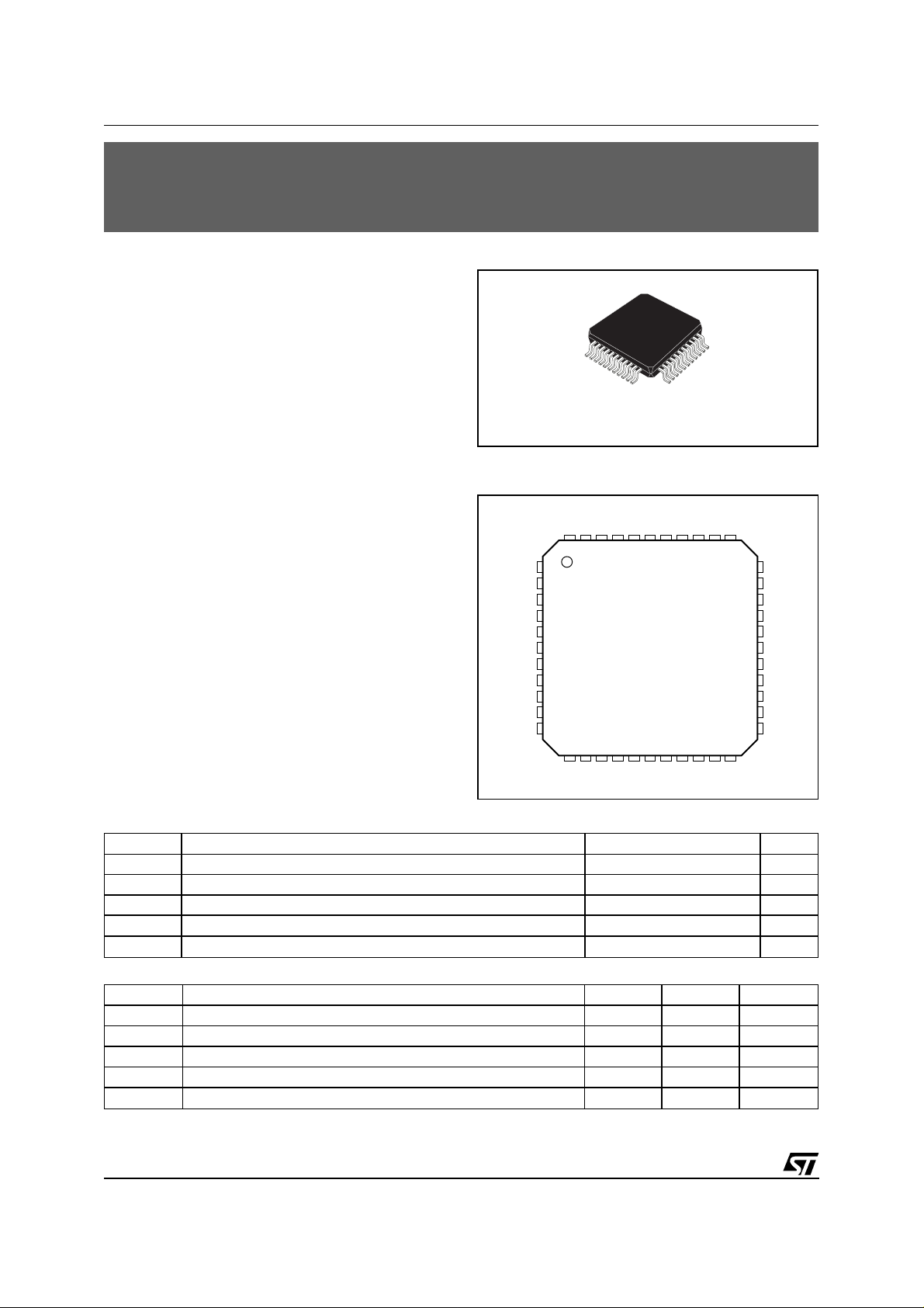
TQFP44
ORDERING NUMBER:
The Kit comprises 2 devices, the L3234 ringing
injector fabricated in Bipolar in 140V Technology.
Its function is to amplify and inject in balanced
mode with zero crossing the ringing signal. The
device requires an external positive supply of
100V and a low level sinusoid of approx.
950mVrms. The L3235N Line Feeder is integrated in 60V Bipolar Technology. The L3235N
provides battery feed to the line with programmable current limitation. The two to four wire voice
frequency signal conversion is implemented by
the L3235N and line terminating and balance impedances are externally programmable. The
L3234/L3235N kit is designed for low power dissipation. In a short loop condition the extra power is
dissipated on an external transistor. The Kit is
controlled by five wire parallel bus and interfaces
easily to all the STLC5046 and STLC5048
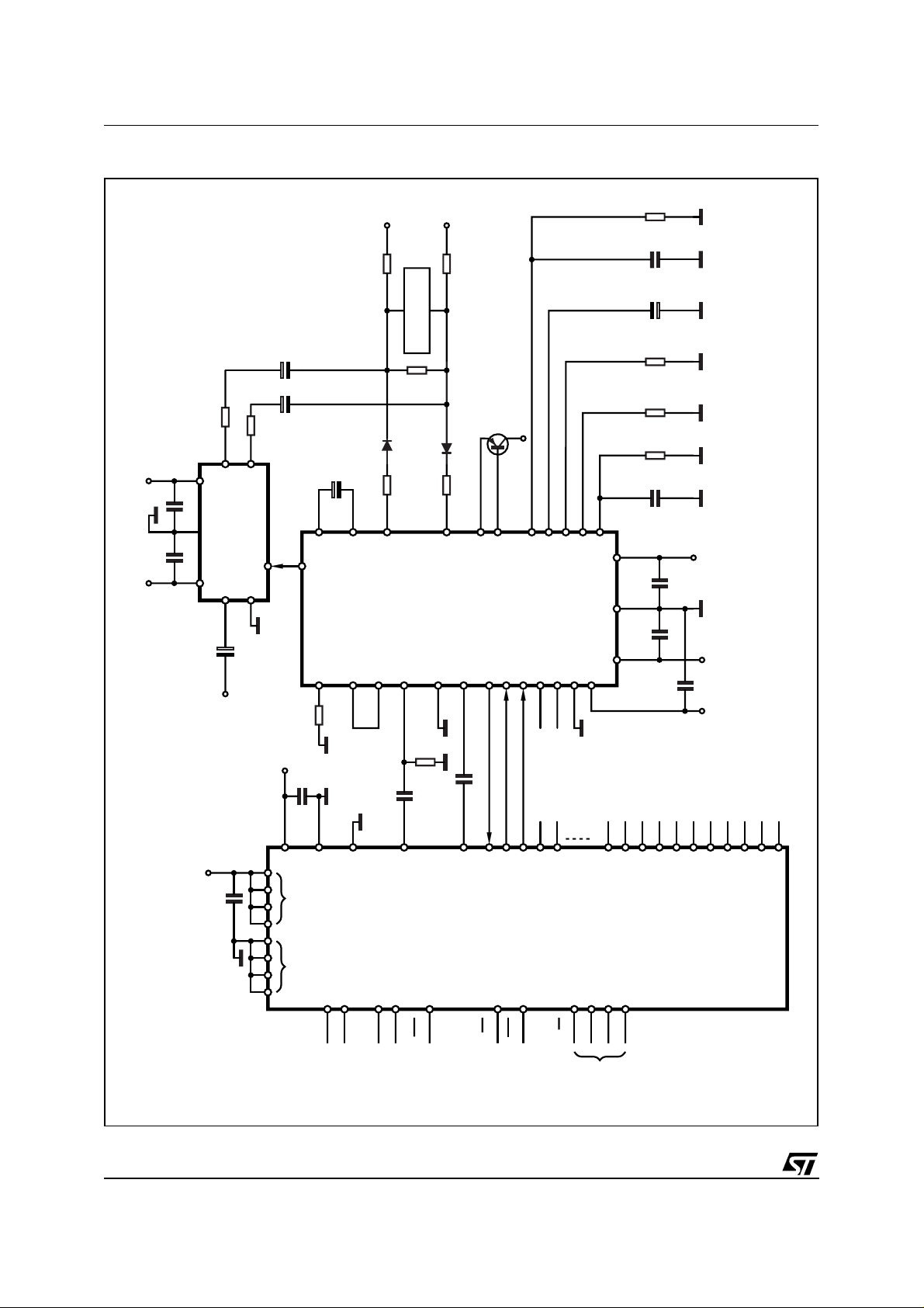
CODECs. In Kit with STLC5048 (see fig 1) the
line impedance synthesis and echo canceling are
performed inside the CODEC.
L3234
L3235N
December 2001
1/25
Page 2
L3234 - L3235N
ABS TYPICAL LINE CARD APPLICATION
CC
V
GND
V100
10µF
82Ω
82Ω
10µF
5
7
0.1µF0.1µF
L3234
2
63
1
4
VA
GND
CS
CAC
CS
29
D1
CAC
100µF
IL
6
18
4.7µF
7
43
ZAC
VRING
ZS=4100Ω
DD
V
0.1µF
DD
V
VSSSUB
CC
CC
V
CC
0.1µF
V
20Ω
P2
R
1N4007
30Ω
TIP
11
ZA
TIP
38
PROTECTION
OVERVOLTAGE
RT
1MΩ
D2
1N4007
P1
R
30Ω
RING
10
12
ZB
RX
100K
100µF
VFRO0
RING
20Ω
P2
R
P1
R
40
L3235N
9
TX
VFXI0
TEXT
VREG
BASE
44
22
31
OH
RNG
CTX 100nF
IO0
IO1
MJE350
V
RTF
25
27
SBY
IO2
BAT
VPOL
34
28
PUNEG
IO3
LIM
20
32
GDK
IO4
REF
GKF
241435
3
13
CC
V
BGND
BAT
AGND V
17239
SS
V
IO11
IO12(CS0)
RF
39K
CF
390nF
CR
4.7µF
9.1K
RLIM
RR
51K
39K
RGF
CGF
390nF
CVSS CVB
IO13(CS1)
IO14(CS2)
to 35K
0.1µF0.1µF
CVCC
IO15(CS3)
VFRO1
BAT
V
SS
V
0.1µF
CC
V
VFXI1
VFRO2
VFXI2
VFRO3
VFXI3
D98TL381
2/25
TSX
STLC5048
INT
RES
CS
CO
CCLK
SERIAL
CONTROL
CI
PORTS
EE
V
GND V
DX
DR
FS
MCLK
Page 3
L3234
Solid State Ringing Injector
DESCRIPTION
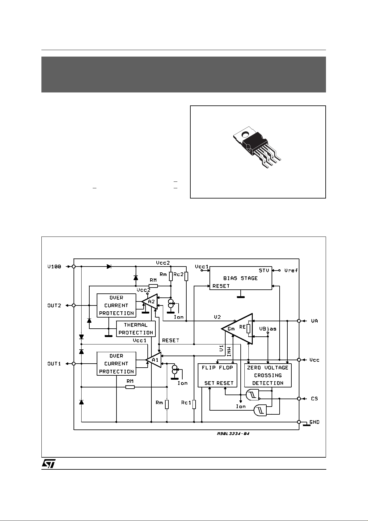
The L3234 is a monolithic integrat ed circuit which
is part of a kit of solid state devices for the subscriber line interface. The L3234 sends a ringing
signal into a two wires analog telephone line in
balanced mode. The AC ringing signal amplitude
is up t o 60Vrms, and for that purpose a positive
supply voltage of +100V shall be available on the
subscriber card.
The L3234 receives a low amplitude ringing signal (950mVrms) and provide the voltage/current
amplification (60Vrms/70mA) when the enable input is active (CS
0.8V) the power consumption of the chip is very
low (<14mW).
The circuit is designed with a high voltage bipolar
technology (V
> 2V). In disable mode (CS <
> 140V / V
CEO
> 250V).
CBO
L3234 - L3235N
HEPTAWATT
The package is a moulded plastic power package
(Heptawatt) suitable also for surface mounting.
BLOCK DIAGRAM
3/25
Page 4
L3234 - L3235N
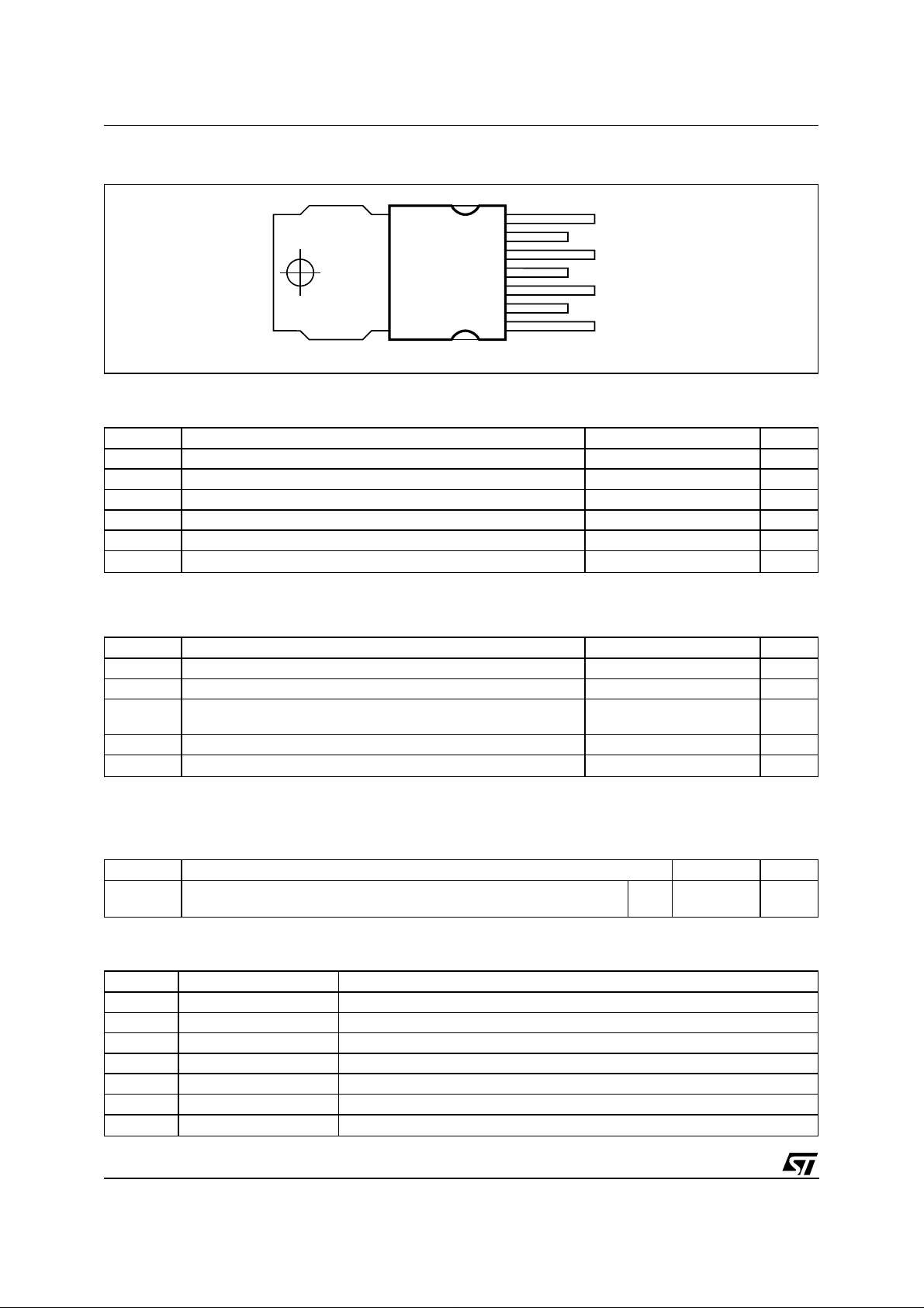
PIN CONNECTION (Top view)
7
6
5
4
3
2
1
D94TL131
OUT2
V100
OUT1
GND
VCC
CS
VA
ABSOLUTE MAXIMUM RATINGS
Symbol Parameter Value Unit
V100 Positive Power Supply Voltage +120 V
V
V
CS Logical Ring Drive Input V
T
T
5V Power Supply Voltage 5.5 V
CC
Low Voltage Ringing Signal (with V100 = 120Vdc) 1.4 Vrms
A
CC
Max. Junction Temperature 150
j
Storage Temperature -55 to +150
stg
OPERATING RANGE
Symbol Parameter Value Unit
V100 High Power Supply Voltage 95 to 105 V
V
V
T
T
Low Power Supply Voltage 5 ±5% V
CC
Low Voltage Ringing Signal
A
Operating Temperature for
op
Max. Junction Operating Temperature (due to thermal protection) 130
jop
L3234
600 to 950
within 10Hz - 100Hz
0 to 70
o
C
o
C
Vrms
C
°
C
°
Note:
Operating ranges define those limits between which the functionality of the device is guaranteed.
THERMAL DATA
Symbol Description Value Unit
R
th j-case
R
th j-amb
Thermal Resistance Junction-case
Thermal Resistance Junction-ambient
Max.
Max.
4
50
PIN DESCRIPTION
Pin Name Description
1 VA Low Voltage Ringing Signal Input
2 CS Logical Ring Drive Input
3V
CC
4 GND Common Analog-Digital Ground
5 OUT1 Ringing Signal Output
6 V100 +100V High Power Supply
7 OUT2 Ringing Signal Output in Opposite Phase with Out1
4/25
+5V Low Power Supply
o
C/W
o
C/W
Page 5
L3234 - L3235N
OPERATION DESCRIPTION
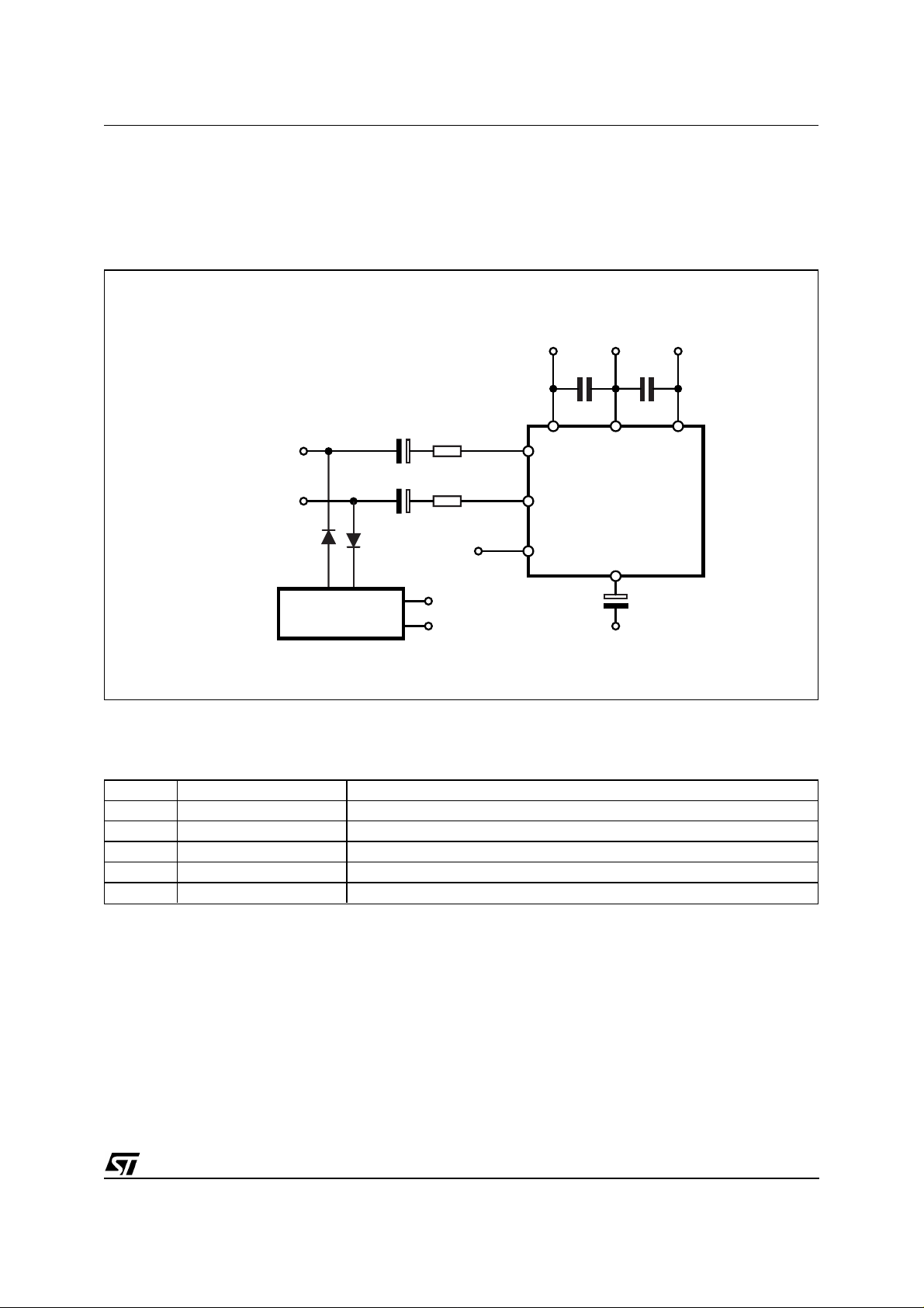
The Fig. 1 show the simplified circuit configuration
Figure 1: L3234/L3235N Circuit Configuration
TIP
A
LINE TERMINALS
RING
LINE FEEDER
CO1
CO2
B
L3235N
of the L3234 Solid State Ringing injector when
used with the L3235N Line Feeder.
+5VGND+100V
C100 CVCC
VCCGNDV100
RO1
OUT1
RO2
OUT2
CS
CS
GND
-VBAT
643
5
RINGING INJECTOR
7
L3234
2
1
VA
CA
D94TL-L3235N
VA
EXTERNAL COMPONENTS LIST
In the following table are shown the recommended external components values for L3234.
Ref. Value Involved Parameter or Function
R01, R02 82
C01, C02 10µF - 160V Ringing Feeding De coupling Capacitors
CA 4.7µF - 10V Low Level Ringing Signal De coupling Capacitor
C100 100nF - 100V Positive Battery Filter
CV
CC
Ω
100nF +5V Supply Filter
When the ringing function is selected by the subscriber card, a lo w level sig nal is contin uously applied to pin 1 t hr o ugh a de cou pling ca pacitor . T h en
the logical rin g drive sign al CS provide d by L3235N
is applied to pin 2 with a cadenced mode.
The rin ging cycles a re synchronis ed by the L3234
in such a way that the r inging start s and stops always when the analog input signal crosses zero.
When the ringing injection is enabled (CS = "1"),
an AC ringing signal is injected in a balanced
Ringing Feeding Series Resistors
mode into the telephone line.
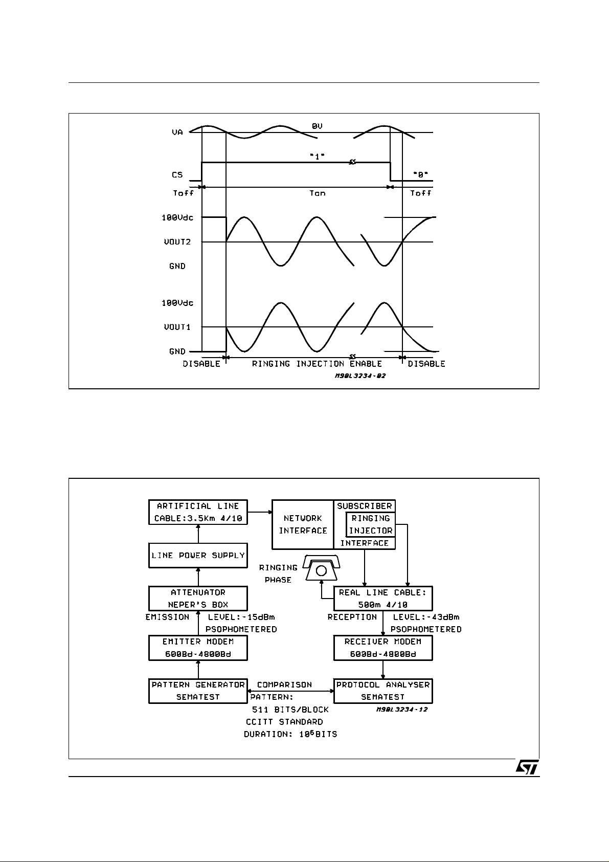
When the ringing injection is disabled (CS = "0"),
the output voltage on OUT2 raises to the high
power supply, whereas on OUT1, it falls down to
ground.
The L3234 has a low output impedance when
sending the signal, and high output impedance
when the ringing signal is disabled
In fig. 2 the dynamic features of L3234 are
shown.
5/25
Page 6
L3234 - L3235N
Figure 2: Dynamic Features of L3234
DATA TRANSMISSION INTERFERENCE TEST
The L3234 meet the requirements of the technical
specification ST/PAA/TPA/STP/1063 from the
CNET. The test circuit used is indicated below.
The measured error rate for data transmission is
lower than 10
This test measures if during the ringing phase the
circuit induce any noise to the closer lines.
Figure 3: Test Circuit Data Transmission Interference Test
-6
during the ringing phase.
6/25
Page 7
L3234 - L3235N
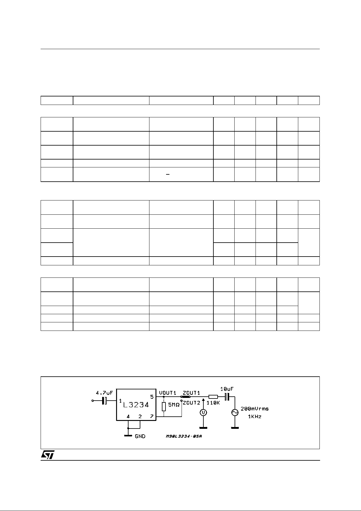
ELECTRICA L CHARA CTERI STI CS (Test conditions: V100 = +100V, V
= +5V, T
CC
= 25°C, unless oth-
amb
erwis e s pecifi ed)
Note: Testing of all parameter is performed at 25°C. Characterisation, as well as the design rule used al-
low correlation of tested performance with actual performances at other temperatures. All parameters listed here are met in the range 0°C to +70°C.
Symbol Parameter Test Condition Min. Typ. Max. Unit Fig
STAND BY MODE: CS = "0"
IS (V100)
I
(VCC)
S
V
SOUT1
V
SOUT2
Z
SOUT1
Z
SOUT2
THD Harmonic Distortion During
Consumption VA = 950mVrms; 50Hz 45
560
100
800
DC Output Voltage VA = 950mVrms; 50Hz
92
Output Impedance 70
70
Z
Matching 15 %
OUT
< 6dBm; f = 1kHz -46 -40 dB 5
V
LINE
Emission
A
µ
A
µ
6V
V
k
Ω
k
Ω
4
RINGING PHASE: CS = "1"
DC OPERATION
IR (V100)
I
(VCC)
R
V
ROUT1
V
ROUT2
V
IH
IIH (CS = 0)
V
IL
IIL (CS = 0)
I
lim
Consumption Z
DC Output Voltage VA = 0V 44
Threshold Voltage on the
Logical Input CS
DC Line Current Limitation VA = 0V 70 150 mA 12
=
∞
LINE
VA = 950mVrms; 50Hz
44
VA = 950mVrms; 50Hz 2.0
2.5
2.2
5
3
56
56
1
0.8
1
mA
mA
V
V
V
µ
V
µ
A
6
A
AC OPERATION
V
/VA
OUT1
V
/VA
OUT2
V
OUT1 -VOUT1
Ringing Gain Z
Ringing Signal ZLINE = 2.2µF + 1k
= 2.2µF + 1k
LINE
VA = 0dBm
Ω
29.5
29.5
Ω
57 60 Vrms
30
30
VA = 950mVrms; 50Hz
THD V
(VA) Input Impedance VA = 950mVrms; 50Hz 40 k
Z
IN
Z
OUT
Harmonic Distortion VA = 950mVrms; 50Hz 5 %
LINE
Differential Output Impedance I
< 50mArms 20
LINE
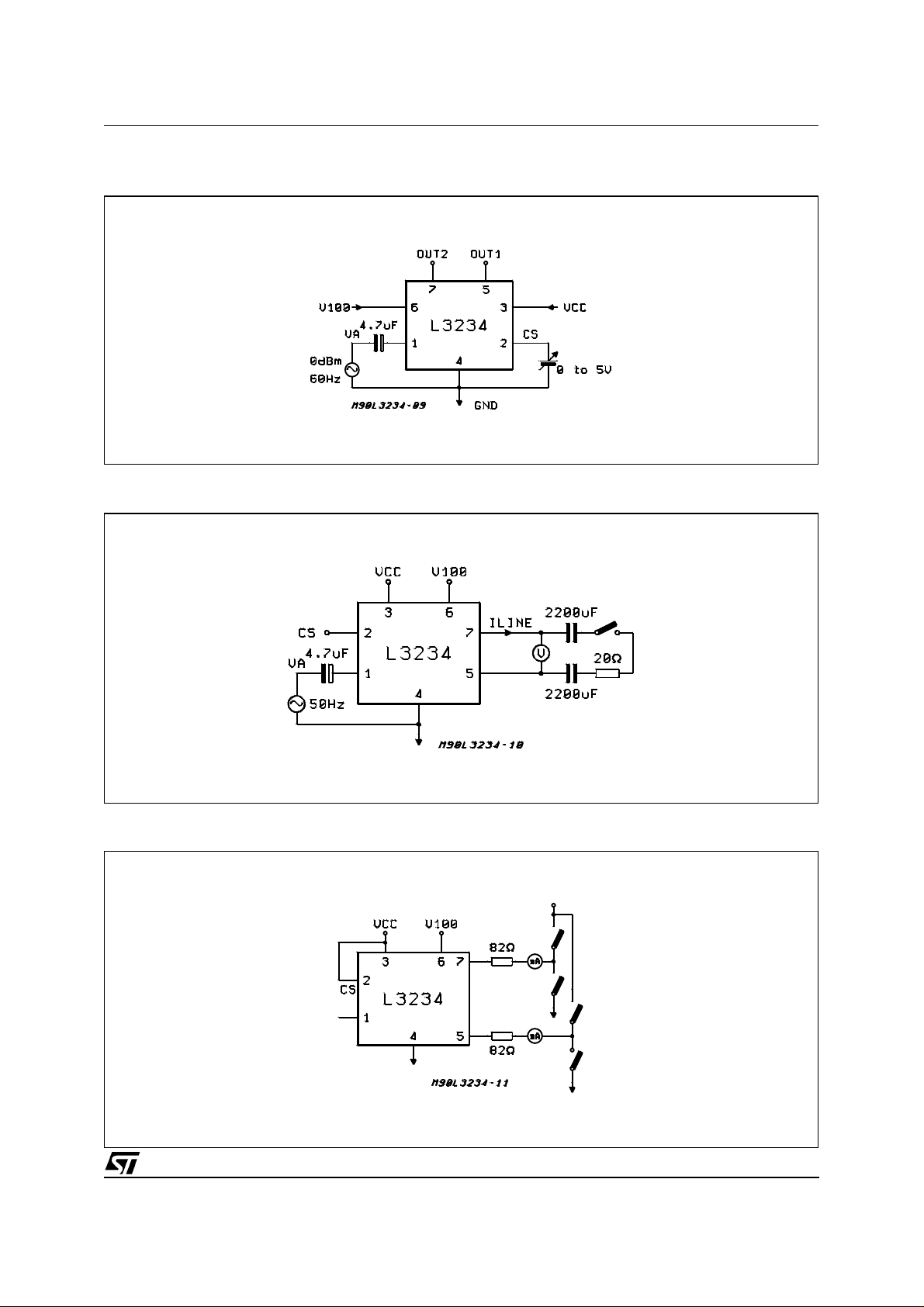
TEST CIRCUITS
Figure 4.
dB
dB
Ω
7
7
Ω
8
9
7/25
Page 8
L3234 - L3235N
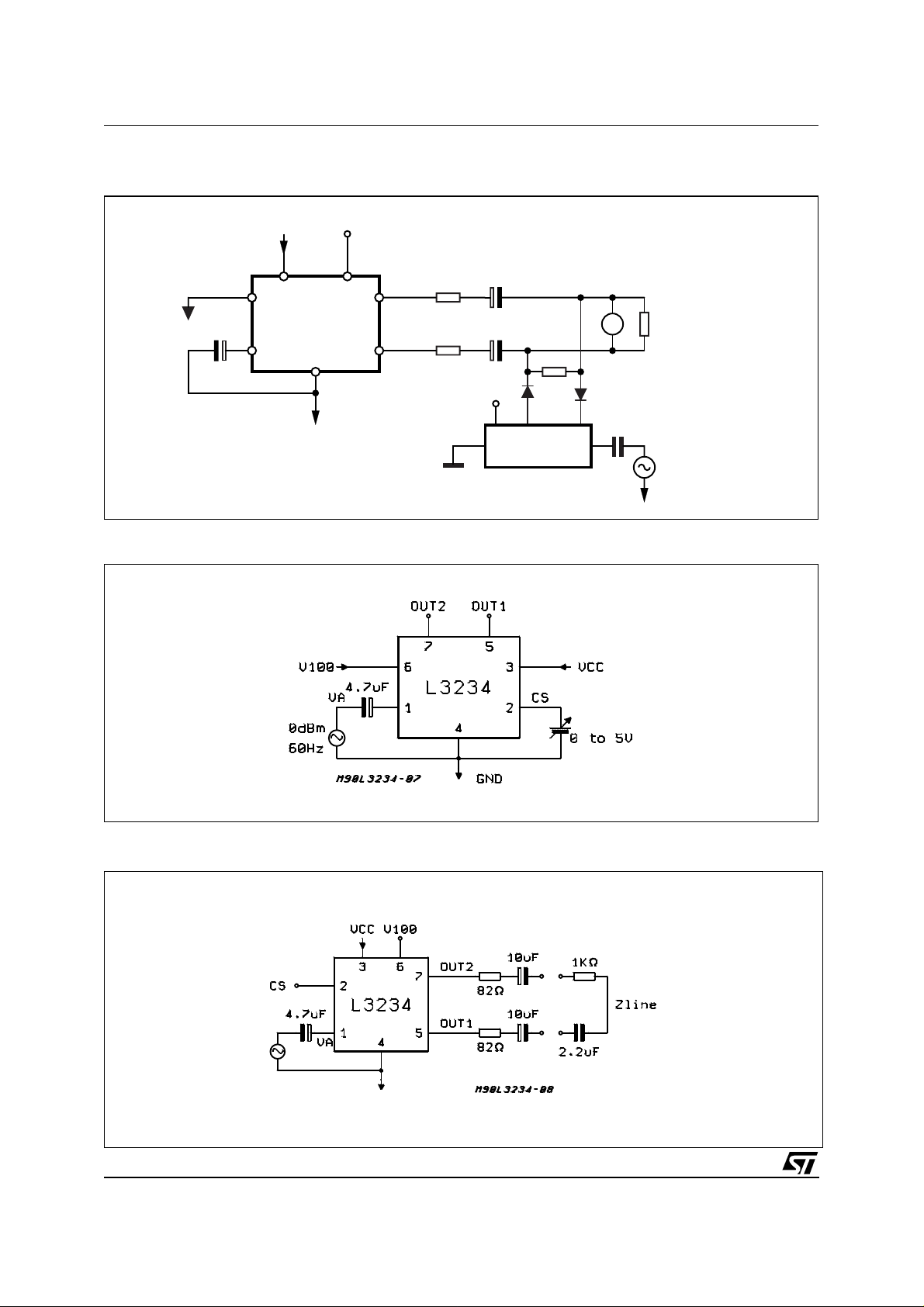
TEST CIRCUITS (continued)
Figure 5.
VCC V100
Figure 6.
4.7µF
CS
2
1
L3234
4
GND
D94TL133
VOUT2
63
7
VOUT1 A
5
82Ω
82Ω
10µF/160V
10µF/160V
-VBAT
LINE FEEDER
1MΩ
B
V
ZLINE=600Ω
VE 1KHz
Figure 7.
8/25
Page 9
TEST CIRCUITS (continued)
Figure 8.
Figure 9.
L3234 - L3235N
Figure 10.
9/25
Page 10
L3234 - L3235N
L3235N
Subscriber Line Interface Circuit
DESCRIPTION
Circuit description
The L3235N Subscriber Line Interface Circuit
(SLIC) is a bipolar integrat ed circuit in 60V technology optimized for PABX application.
The L3235N supplies a line feed voltage with a
current limitation which can be modified by an external resistor (RLIM).
The SLIC incorporates loop currents, ground key
detection functions with an externally programmable constant time.
The two to four wires and four t o two wires voice
frequency signal conversion is performed by the
L3235N and the line terminating and the balancing impedances are externally programmable.
The device integrates an automatic power limitation circuit. In short loop condit ion the extra power
is dissipated on one external transistor (Text).
This aproach allows to assembly the L3235N in a
low cost standard plastic TQFP44 package.
The c hip is protec ted b y ther mal prot ecti on at
Tj = 150°C.
The SLIC is able to give a power up command for
Combo in off hook condition and an enable logic
for solid state ringing injector L3234.
The L3235N package is 44 pin plastic TQFP.
The L3235N has been designed to operate
togheter with L3234 performing complete
BORSHT function without any electromechanical
ringing relay (see the application circuit fig. 16).
PIN CONNECTION
ZAC
VREG
44 43 42 41 3940 38 37 36 35 34
1
N.C.
2
AGND
3
BGND
4
N.C.
5
N.C.
6
CAC
7
RPC
8
N.C.
9
TX
ZB
10
ZA
12 13 14 15 16
CC
RX
V
N.C.
REF
N.C.
N.C.
TQFP44
RING
N.C.
bat
TIP
V
171118 19 20 21 22
IL
SS
V
N.C.
N.C.
N.C.
VPOL
GKF
N.C.
RTF
33
32
31
30
29
28
27
26
25
24
23
BASE
N.C.
GDK
OH
N.C.
CS
PU
SBY
N.C.
RNG
LIM
N.C.
D99TL456
ABSOLUTE MAXIMUM RATINGS
Symbol Parameter Value Unit
V
BAT
V
CC
V
SS
T
T
stg
Battery Voltage -54 V
Positive Supply Voltage 5.5 V
Negative Supply Voltage -5.5 V
Max. Junction Temperature 150 °C
j
Storage Temperature -55 to +150 °C
OPERATING RANGE
Symbol Parameter Min. Max. Unit
V
BAT
V
CC
V
SS
T
op
T
Note:
Operating ranges define those limits between which the functionality of the device is guaranteed.
10/25
Battery Voltage -52 -24 V
Positive Supply Voltage 4.75 5.25 V
Negative Supply Voltage -5.25 -4.75 V
Operating Temperature for
Max Junction Operating Temperature 130 °C
j
L3235N
070°C
Page 11
L3234 - L3235N
THERMAL DATA
Symbol Description Value Unit
R
th j-amb
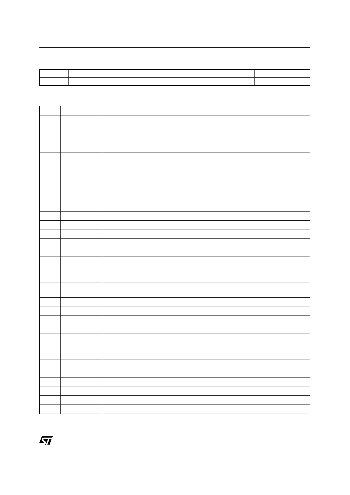
PIN DESCRIPTION
N° Name Description
1,4,5,8,
15,16,19
,21,23,
26,30,33
,36,37,
41,42
2 AGND Analog/Digital Ground.
3 BGND Battery Ground. This is the Reference for the Battery Voltage (note 1).
6 CAC AC Current Feedback Input.
7 RPC External Protection Resistors AC Transmission Compensation.
9 TX Four Wire Transmitting Amplifier Output.
10 ZB Non Inverting Operational Input Inserted in the Hybrid Circuit for 2W to 4W Conversion.
11 ZA VRX Output Buffer 2W to 4W Conversion.
12 RX High Impedance Four Wire Receiving Input.
13 V
14 REF Voltage Reference Output; a Resistor Connected to this pin sets the Internal Bias Current.
17 V
18 IL Transversal Line Current Feedback Divided by 50.
20 VPOL Non Inverting Operational Input to Implement DC Character.
22 BASE Driver for External Transistor Base.
24 LIM Voltage Reference Output; a Resistor Connected to this Pin Sets the Value of Line
25 RNG Ringing Logic Input from Line Card Controller.
27 SBY Stand by Logic Input (SBY = 1 Set Line Current Limitation at 3mA).
28 PU Power u.p Logic Output for the Codec Filter. (PU = 0 means Codec Filter Activated)
29 CS Ring Injector Enable for L3234 Output. (CS = 1 means L3234 Ringing Injection Enable).
31 OH Hook Status Logic Output (OH = 0 means off hook).
32 GDK Ground Key Status Logic Output (GDK = 0 means Ground Key on).
34 RTF Time Constant Hook Detector Filter Input.
35 GKF Time Constant GK Detector Filter Input.
38 TIP Tip Wire of 2 Wire Line Interface.
39 V
40 RING RING wire of 2 Wire Line Interface.
43 ZAC Non Inverting Input of the AC Impedance Synthesis Circuit.
44 VREG Emitter Connection for the External Transistor.
Thermal Resistance Junction-ambient Max 60 °C/W
NC Not Connected
The Network Connected from this Pin to Ground shall be a copy of the Line Impedance.
CC
SS
Positive 5V Supply Voltage.
Negative 5V Supply Voltage.
Current Limitation.
bat
Negative Battery Supply Input.
Note 1:
AGND and BGND pins must be tied together at a low impedance point (e.g. at card connector level).
11/25
Page 12
L3234 - L3235N
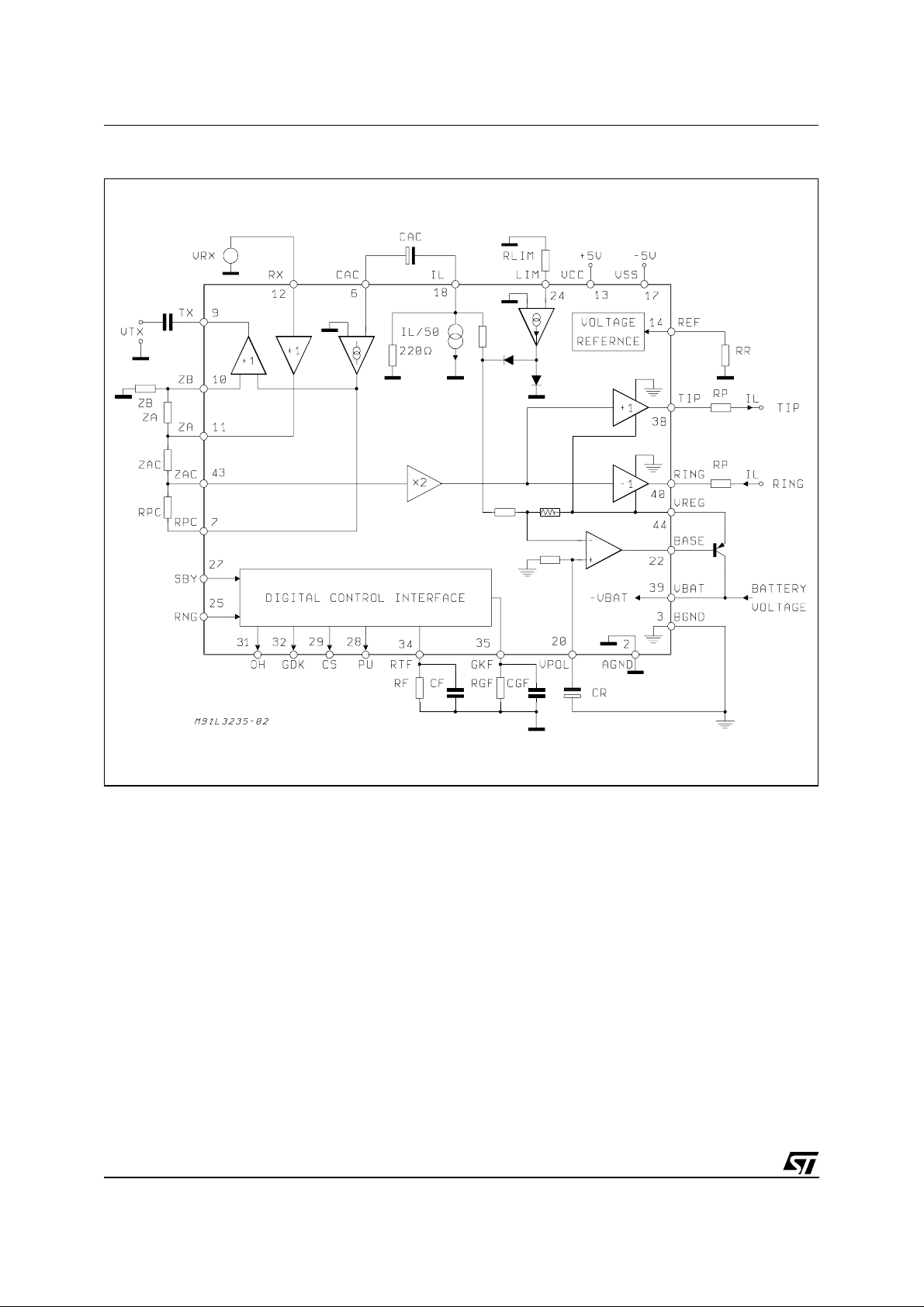
L3235N FUNCTIONAL DIAGRAM
FUNCTIONAL DESCRIPTION
DIGITAL INTERFACE
The different operating modes of the L3235N are
programmed through a digital inter face based on
two input pins:
1)SBY input programs the stand-by or Active/Ringing modes.
2)RNG input programs the ringing ON/OFF activation condition for the L3234.
The L3235N digital interface has four output pins :
1)OH provides the on hook/off hook or ring trip
informations (active low).
2)GDK provides the ground key on/off information (active low).
3)PU must be connected to the enable input pin
of CODEC/FILTER devices like ETC 5054/57
12/25
and automatically activates this device when
in active mode off-hook is detected or when
ringing mode is selected.
4)CS output must be connected to the CS enable input of the solid state ringing injector
L3234.
In this way the L3234 will be enabled when ringing mode is programmed and will be automatically disabled when the ring trip condition will be
detected reducing the ringing signal disconnection time after ring trip.
The table 1 here below resumes the dif ferent operation modes and the relative logic output signals.
The two current detection (hook and GND key)
have internal fixed threshold. Externally it is possible to program their time costant through two R-C
components connected respectively to pin 26
(RTF) and pin 27 (GKF).
Page 13
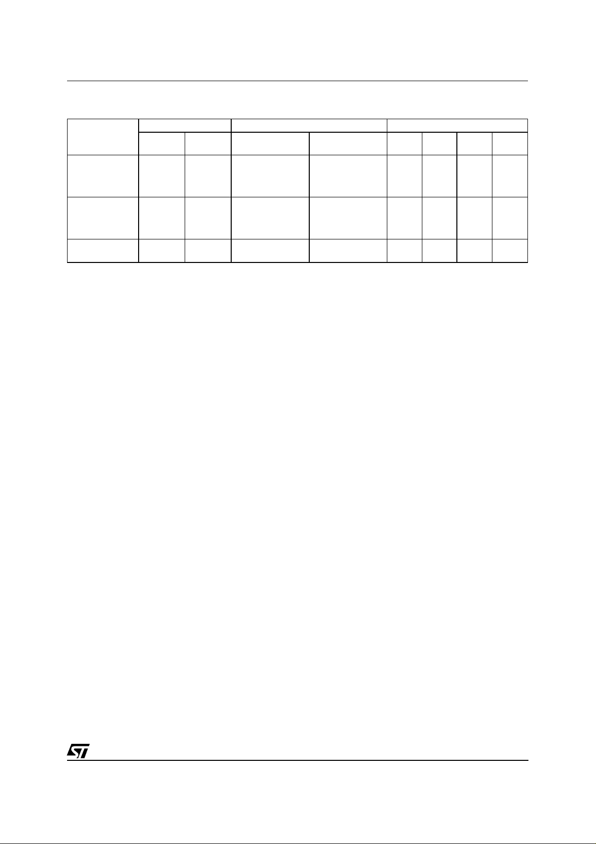
Table 1.
L3234 - L3235N
OPERATING
MODE
ACTIVE
RINGING
STAND-BY
(*)This status is latched and doesn’t change until RNG turn to 0
INPUT PIN LINE STATUS OUTPUT PIN
SBY RNG
0
0
0
0
0
0
0
0
1
1
0
0
0
0
1
1
1
1
0
1
0: ON HOOK
1: OFF HOOK
0
0
1
1
0
0
1
1
X
X
OPER A TING MODES
Stand-B y
(SBY = 1 and RNG = 0)
In Stand-By mode the L3235N limits the DC Loop
current to 3 mA.
In this mode all the AC circuits are active and all
the AC characteristics are the same as in Active
Mode.
Also the two Line Current detectors (hook and
GND key) are active but due to the loop current
limited to 3 mA they will not be activated.
This mode is useful in emergency condition when
it is very important to lim its the system power dissipation.
Ringing Mode
(SBY = 0 and RNG = 1)
When ringing mode is selected "CS" pin is set to
1 in order to activate the L3234 ringing injector.
See L3234 for detailed description.
Ring trip is detected by means of the same inter-
nal circuitry used for off-hook detection.
1
⁄
F
An off-hook delay time lower than
2
RING
should
be selected. (see ext. components list).
When ring trip is detected "CS" is automatically
set to "0" allowing in this way a quick ringing disconnection.
After Ring trip detection the Card Controller must
set the L3235N in active mode to remove the internal latching of the "CS" information.
0: NO GND KEY
1: GND KEY ON
0
1
0
1
0
1
0
1
X
X
Active mode
OH GDK PU CS
1
0
0
0
1
0
0
0
1
1
1
0
1
0
1
0
1
0
1
1
(SBY = 0 and CS1 = 0)
1
0
0
0
0
0
0
0
1
0
0
0
0
0
1
0(*)
0(*)
0(*)
0
1
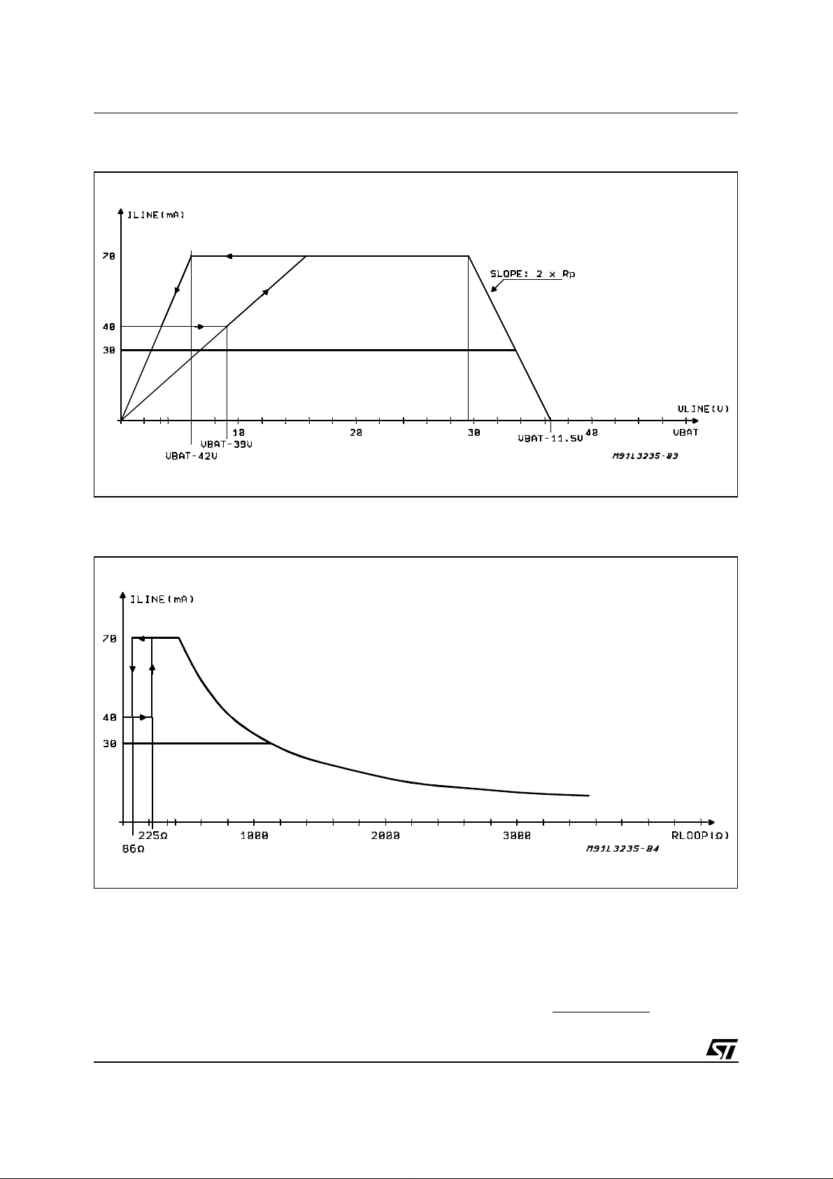
In Active mode the L3235N has the DC characteristic show in Fig.13
The DC characteristics of L3235N has two different feeding conditions:
1)Current Limiting Region : (short loop) the DC
impedance of the SLIC is very high (>20
Kohm) therefore the system works as a current generator. By the ext. r esistor RLIM connected at pin 19 it is possible to program limiting current values from 20 mA to 70 mA.
2) Voltage source region (long loop).
The DC impedance of the L3235N is almost
equal to zero therefore the system works like
a voltage generator with in series the two external protection resistors Rp.
When a limiting current value higher than 40 mA
is programmed the device will automatically reduce to 40 mA the loop current for very short
loop.
This is done in order to lim it the maximum power
dissipation in very short loop to values lower than
2W for the external transistor and lower than
0.5W for the L3235N itself.
This improve the system reliability reducing the
L3235N power dissipation and therefore the internal junction temperature.
13/25
Page 14
L3234 - L3235N
Figure 11:
Figure 12:
DC characteristic in Active Mode with two different values of limiting current (30mA and 70 mA).
Line current versus loop resistance with two different values of limiting current (30mA and
70mA)
AC transmission circuit stability
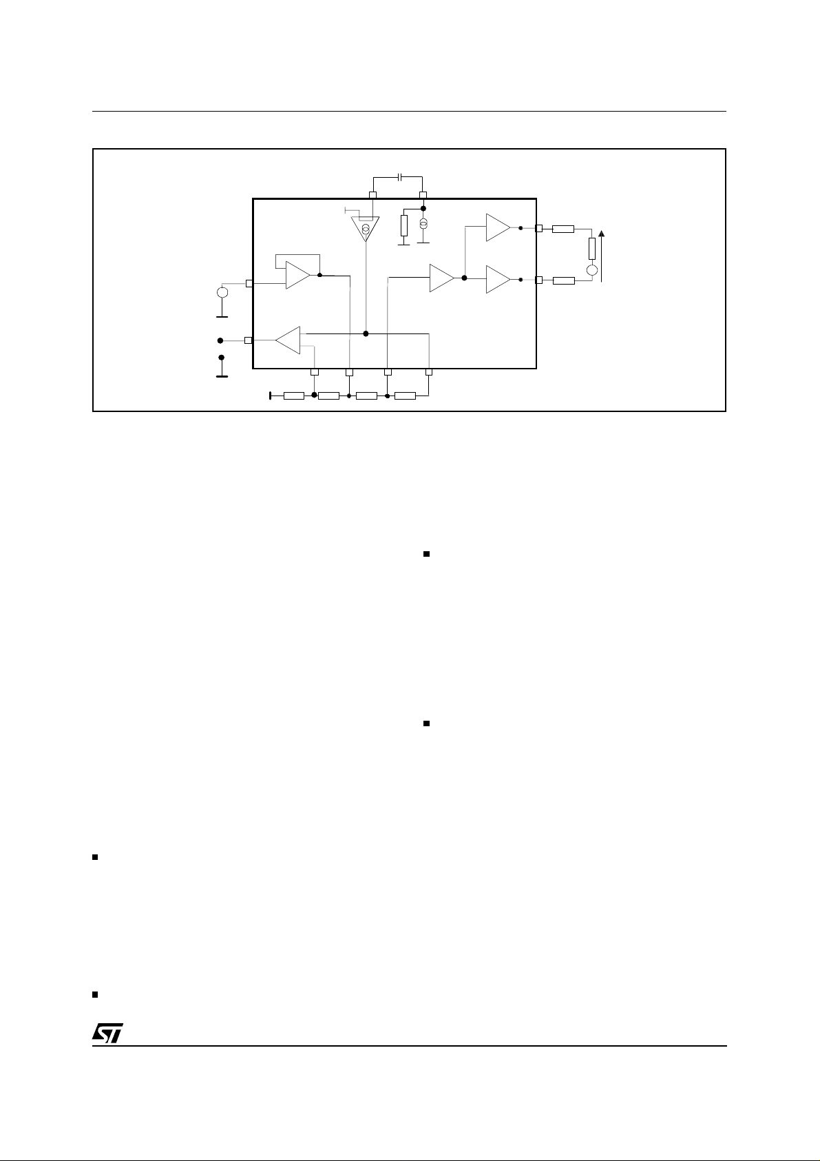
To ensure stability of the feedback loop shown in
block diagram form in figure 13 two capacitors are
required. Figure 14 includes these capacitors Cc
and Ch.
14/25
AC - DC separation
The high pass filter capacitor C
provides the
AC
separation between DC circuits and AC circuits. A
CAC value of 100mF will position the low end frequency response 3dB break point at 7Hz,
fsp =
2
π
⋅
220
1
Ω ⋅
C
AC
Page 15
g
Figure 13.
L3234 - L3235N
Cac
Cac
6
IL'/50
RX
Vrx
TX
Vtx
-
12
+
+
9
1
-
ZB
11
10
ZA
43
ZAC
AC Characteristic
A simplified AC model of the t ransmission circuits
is shown in figure 13
Where:
V
V
V
E
Z
R
is the received signal
rx
is the transmitted signal
tx
is the AC transversal voltage in line
l
is the line open circuit AC voltage
G
is the line impedance
L
are the protection resistors
P
ZB is the line impedance balancing network
Z
Z
is the SLIC impedance balancing network
A
programmable AC line termination
AC
impedance
R
used for external protection resistors
PC
insertion loss compensation
/50 is the AC transversal current divided by 50
I
l
CAC AC feedback current decoupling
AC behavior
The AC path simplified formulas, that are valid
when Il/50’ is equal to Il/50, are the following :
Two wire impedance
The impedance presented to the two wire by
the SLIC including the protection resistors RP
and defined as Zs is equal to :
Zs = ZAC/12.5 + 2RP
i.e. with ZAC = 6250 W and Rp = 50 W
Zs = 600 W
Two wire to four wire gain
The transmission gain , Gtx, of the SLIC is
RPC
IL
18
IL/50
X2
7
+1
-1
L3235N
TIP
RP
38
Zl
RING
40
RP
Vl
E
equal to :
GTX = Vtx / Vl
GTX = 0.25 * (RPC + ZAC) / (25RP + ZAC)
using RPC = 25RP , as recommended to
compensate the protection resistor RP,
GTX = 0.25 (-12 dB)
Four wire to two wire gain
The receiver gain , Grx, of the SLIC is equal to:
GRX = Vl / Vrx
GRX = 50Zl / (ZAC +12.5(Zl + 2RP))
using ZAC = 12.5(Zs - 2RP) and assuming
Zl = Zs we have the following gain:
GRX = 2 (+6 dB)
Hybrid function
The transybrid loss, Thl, is equal to:
Thl = V
tx
/ V
rx
Thl = ZB / (ZA + ZB)-(ZAC +RPC) / (ZAC +
+ 12.5(2R
using Z
= 12.5(ZS - 2RP) and RPC = 25R
AC
+ Zl))
P
we have the following relation:
Thl = Z
/ (ZA + ZB) - Zl / (Zl + Zs)
B
To maximize the hybrid attenuation the impedance must be matched, Z
/ ZB = ZS / Zl, to
A
guarantee Thl = 0.
From th e ab ove rela tion i t is e vident that if Z
equal to the Z
Z
can be substituted by two equal resistors.
B
in Thl test the impedance ZA and
l
P
is
s
15/25
Page 16
L3234 - L3235N
External components list for L3235N
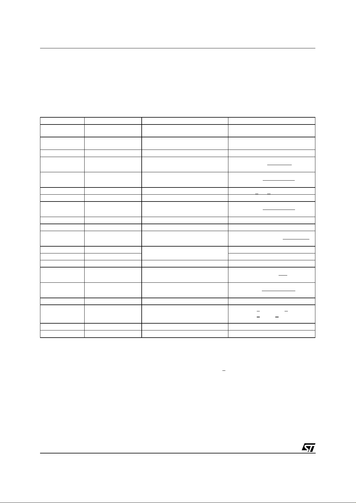
To set the SLIC into operation the following parameters have to be defined:
- The AC SLIC impedance at line terminals "Zs" to which the return loss measurements is referred. It can
be real (typ. 600Ω) or complex.
- The equivalent AC impedance of the line "Zl" used for evaluation of the trans-hybrid loss performance
(2/4 wire conversion). It is usually a complex impedance.
- The value of the two protection resistors Rp in series with the line termination.
Once, the above parameters are defined, it is possible to calculate all the external components using the
⋅ 39KΩ
564
− 3mA
1
Ω ⋅
1
Ω ⋅
=
C
2πf1 ⋅ 25R
Z
AC
Z
AS
1
> 60V
CEO
f
load
Ω
fp
sp
1
P
following table. The typical values has been obtained supposing: Zs = 600Ω; Zl = 600Ω; Rp = 50
Name Suggested Value Function Formula
R
F
C
F
R
GF
C
GF
R
R
R
LIM
39KΩ
390nF
39KΩ
390nF
51KΩ Bias Set
8.4KΩ to 33KΩ Ext. Current Limit. Progr.
CR 4.7µF
6.3 V 30%
R
P
R
T
C
AC
50 Protection Resistors 47 < RP < 100Ω (2)
1MΩ 20% Termination Resistor
100µF
6.3V 20%
R
PC
Z
AC
C
C
Z
AS
R
AS
ZB 15K
C
H
C
TX
1250Ω 1% RP insertion loss compensation RPC = 12.5 ⋅ (2RP)
6250Ω 1% 2W AC Impedance programmation ZAC = 12.5 ⋅ (ZS - 2RP)
470pF 20% AC Feedback compensation
12500Ω 1% Slic Impedance Balancing Net. ZAS = 25 ⋅ (ZS - 2RP)
2500Ω 1% RAS = 25 ⋅ (2RP)
1% Line impedance Balancing Net. ZB = 25 ⋅ Zl
Ω
220pF 20% CC Transybrid loss Compensation
4.7µF 30% DC Decoupling Tx Output
D1, D2 1N4007 Line Rectifier
Text (3) External Transistor P
CV
; CV
SS
DD
C
VB
Notes:
1) For proper operation Cf should be selected in order to verify the following conditions:
A) cf > 150nF
B) τ < 1/2 • f
f
RING
2) For protection purposes the RP resistor is usually splitted in two part R
3) ex: BD140; MJE172; MJE350.... (SOT32 or SOT82 package available also for surface mount). For low power application (reduced battery
voltage) BCP53 (SOT223 surface mount package) can be used. Depending on application envirom ent an heatsink could be neces sary.
RING
: Ringing signal frequency
100nF ±5V supply filter
100nF/100V V
Delay Time
On-hook Off-hook
Delay Time
GK Detector
Negative Battery
Filter
DC/AC current feedback splitting
supply filter
BAT
and RP2, with RP1 > 30Ω.
P1
τ = 0.69 ⋅ C
⋅ 39KΩ (1)
F
τ = 0.69 ⋅ C
R
=
LIM
I
LIM
C
=
AC
2π ⋅
=
C
AC
2π ⋅
f1 = 300KHz C
C
= CC ⋅
H
=
C
TX
6.28 ⋅ fp ⋅ Z
> 2W, V
Diss
H
> 40, IC > 100mA
FE
V
< 0.8V @ 100mA
BE
GF
16K
220
16/25
Page 17
L3234 - L3235N
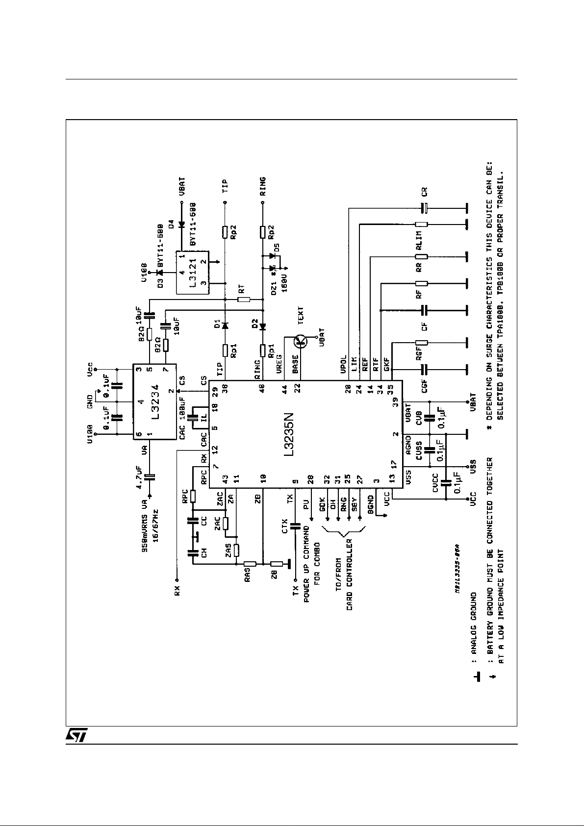
Figure 13:
Typical Appication Circuit Including L3234 and Protection
17/25
Page 18
L3234 - L3235N
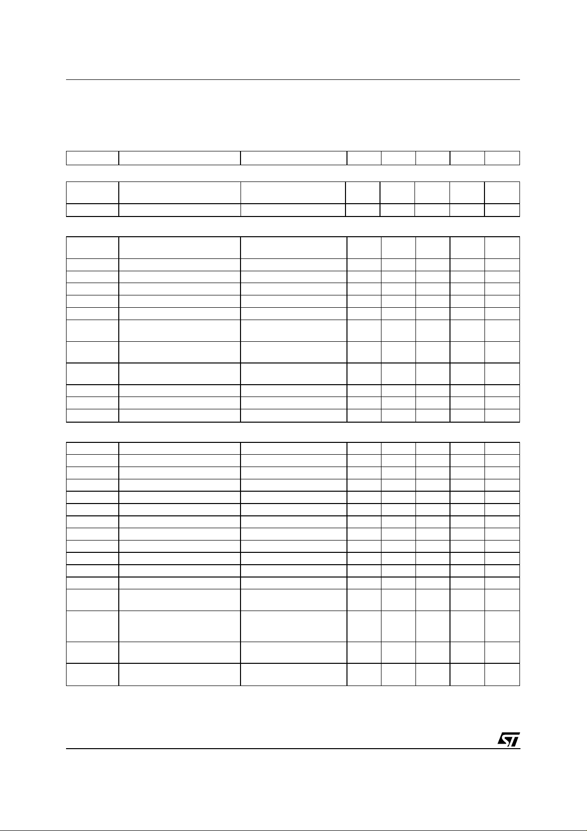
ELECTRICAL CHARACTERISTICS
= -5V, V
V
SS
Note:
Testing of all parameters is performed at 25°C. Characterization, as well as the design rules used
= -48V, T
bat
= 25°C, unless otherwise specified)
amb
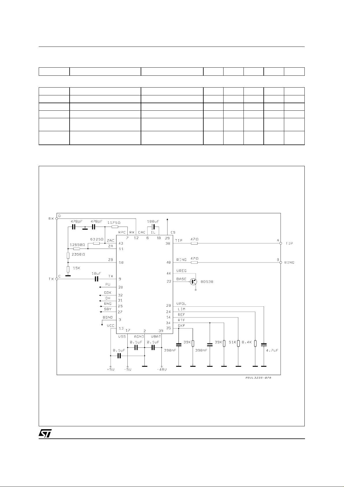
(Test condition: refer to the test circuit of the fig. 16; V
CC
= 5V,
allow correlation of tested performance with actual performance at other temperatures. All parameters listed here are met in the range 0°C to +70°C.
Symbol Parameter Test Condition Min. Typ. Max. Unit Fig.
STAND-BY
I
V
LCC
ls
Output Voltage at TIP/RING
I
= 0 35.7 39 V
LINE
pins
Short Circuit Current Stand-by, SBY = 1 2 3 4 mA
DC OPERATION
V
lP
I
lim
I
lim
I
O
I
f
I
lgk
Gklim Ground Key Current
Gkov Ground Key Threshold
I
max
IV
CC
IV
SS
IV
bat
Output Voltage at TIP/RING
pins
Current Progr. I
Current Progr. 8.4KΩ < R
I
= 0
LINE
I
= 50mA
LINE
Prog. = 70mA 63 70 77 mA
lim
< 33KΩ 20 70 mA
LIM
35.7
35.2
39
39
V
V
On-hook Threshold 5 mA
Off-hook Threshold 10 mA
GK Detector Threshold 10 17 mA
RING to BGND 13 22 mA
Limitation
Gklim-Ilgk 1 mA
Overloap
Max. Output Current at
I
= 70mA 90 140 mA
lim
TIP/RING
Supply Current from V
Supply Current from V
Supply Current from V
CC
SS
bat
I
= 0 6.2 8 mA
line
Iline = 0 1.6 2.1 mA
Iline = 0 2.8 3.6 mA
AC OPERATION
Z
tx
Z
rx
R
l
Sending Output Impedance pin 9 (Tx) 10 Ω
Receiving Input Impedance pin 12 (Rx) 1 MΩ
2W Return Loss f = 300 to 3400Hz 22 36 dB A1
Thl Trans Hybrid Loos f = 300 to 3400Hz 22 36 dB A2
G
s
G
sf
G
sl
G
r
G
rf
G
rl
Sending Gain f = 1020Hz Il = 20mA -11.9 -12.1 -12.3 dB A3
Flatness f = 300 to 3400Hz -0.2 0.2 dB
Linearity -20dB to 10dBm -0.2 0.2 dB
Receiving Gain f = 1020Hz Il = 20mA 5.8 6 6.2 dB A4
Flatness f = 300 to 3400Hz -0.2 0.2 dB
Linearity -20dBm to +4dBm -0.2 0.2 dB
Np4W Psoph. Noise at Tx -90 -78 dBmp
Np2W Psoph. Noise at Line -82 -70 dBmp
S
vrr
S
vrr
Relative to V
versus Line
bat
Terminal versus Tx Terminal
Relative to Vcc and V
ss
versus Line Terminal versus
f = 1020Hz
V
= 100mVpp
S
f = 1020Hz
VS = 100mVpp
-30
-24
-20
-14
Tx Terminal
L
tc
L/T Conversion measured at
line Terminals
T
lc
T/L Conversion Measured at
Line Terminals
(*) Selected parts L3235NC
f = 300 to 3400
I
= 20mA
line
f = 300 to 3400
I
= 20mA
line
49
53(*)
46(*) dB A7
dB
dB
dB
dB
dB
dB
A5
A6
18/25
Page 19
L3234 - L3235N
ELECTRICAL CHARACTERISTICS
(continued)
Symbol Parameter Test Condition Min. Typ. Max. Unit Fig.
DIGITAL STATIC INTERFACE
V
il
V
ih
I
il
I
ih
V
ol
V
oh
Figure 14:
Input Voltage at Logical "0" Input SBY, CS1 0 0.8 V
Input Voltage at Logical "1" Input SBY, CS1 2 5 V
Input Current at Logical "0" Input SBY, CS1 10 µA
Input Current at Logical "1" Input SBY, CS1 10 µA
Output Voltage at Logical "0" I
Output Voltage at Logical "1" I
= 1mA
out
I
= 10µA
out
= 10µA
out
I
= 1mA
out
0.5
0.4
4
2.7
Test Circuit
V
V
V
V
L3235N
19/25
Page 20
L3234 - L3235N
APPENDIX A
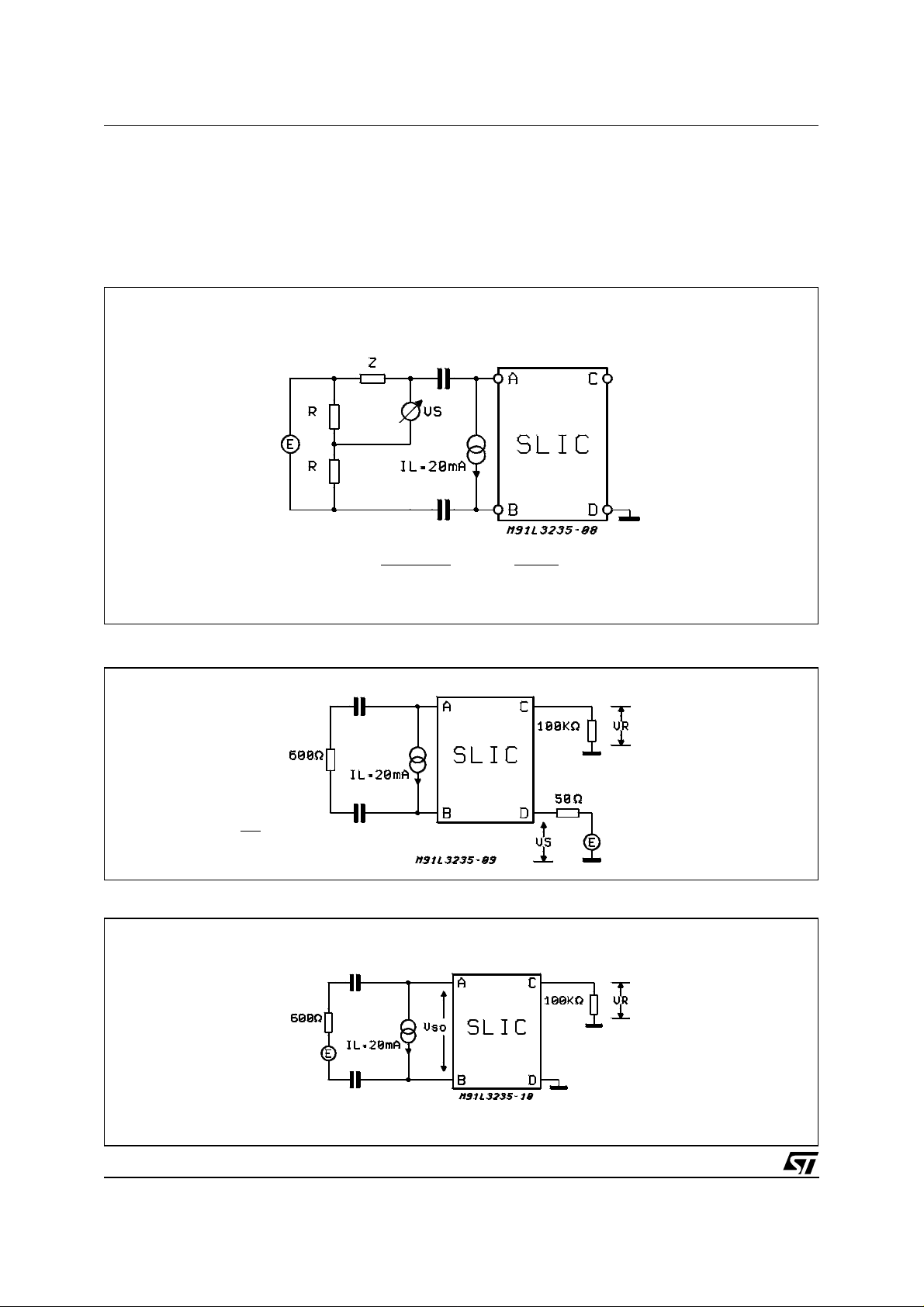
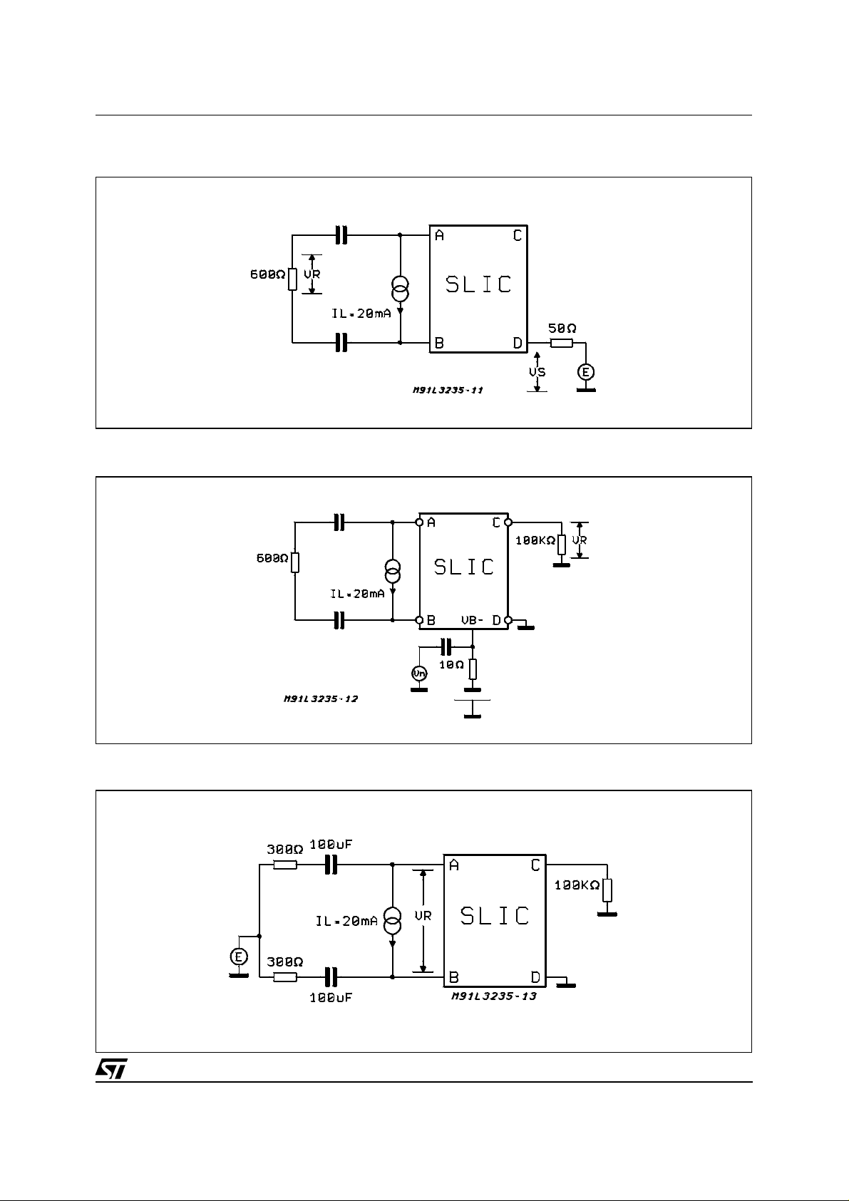
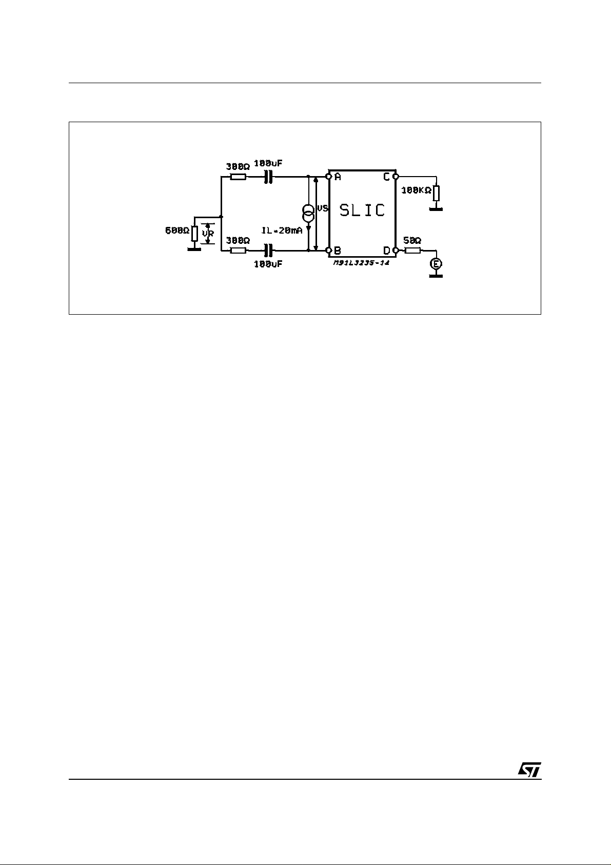
L3235N TEST CIRCUITS
Referring to the test circuit reported in fig 16 you
can find the proper configuration for the main
measurements.
Figure A1:
2W Return Loss
= 20 log
R
L
| Z
| Z
ML
ML
100µF
100µF
− Z |
+ Z |
In particular:
A-B: Line terminals
C: Tx sending output on 4W side
D: Rx receiving input on 4W Side
| 2V
|
= 20 log
| E
S
|
Figure A2:
T
HL
Figure A3:
Trans-hybrid Loss
V
= 20log
S
V
R
Sending Gain
100µF
100µF
100µF
20/25
100µF
Page 21
L3234 - L3235N
TEST CIRCUITS
Figure A4:
Figure A5:
Receiving Gain
SVRR Relative to Battery Voltage VB
(continued)
100µF
100µF
100µF
Figure A6:
100µF
Longitudinal to Transversal Conversion
21/25
Page 22
L3234 - L3235N
Figure A7:
Transversal to Longitudinal Conversion
APPENDIX B
LAYOUT SUGGESTIONS
Standard layout rules should be followed in order
to get the best system performances:
1) Use always 100nF filtering capacitor close to
the supply pins of each IC.
2) The L3235N bias resistor (RR) should be connected
close to the correspondin g pins of L3235N
(REF and AGND).
22/25
Page 23
L3234 - L3235N
DIM.
MIN. TYP. MAX. MIN. TYP. MAX.
A 4.8 0.189
C 1.37 0.054
D 2.4 2.8 0.094 0.110
D1 1.2 1.35 0.047 0.053
E 0.35 0.55 0.014 0.022
F 0.6 0.8 0.024 0.031
F1 0.9 0.035
G 2.41 2.54 2.67 0.095 0.100 0.105
G1 4.91 5.08 5.21 0.193 0.200 0.205
G2 7.49 7.62 7.8 0.295 0.300 0.307
H2 9.2 10.4 0.362 0.409
H3 10.05 10.4 0.396 0.409
L 4.6 5.05 0.181 0.198
L1 3.9 4.1 4.3 0.153 0.161 0.170
L2 6.55 6.75 6.95 0.253 0.265 0.273
L3 5.9 6.1 6.3 0.232 0.240 0.248
L5 2.6 2.8 3 0.102 0.110 0.118
L6 15.1 15.8 0.594 0.622
L7 6 6.6 0.236 0.260
M 0.17 0.32 0.007 0.012
V2 8°(max)
Dia 3.65 3.85 0.144 0.152
mm inch
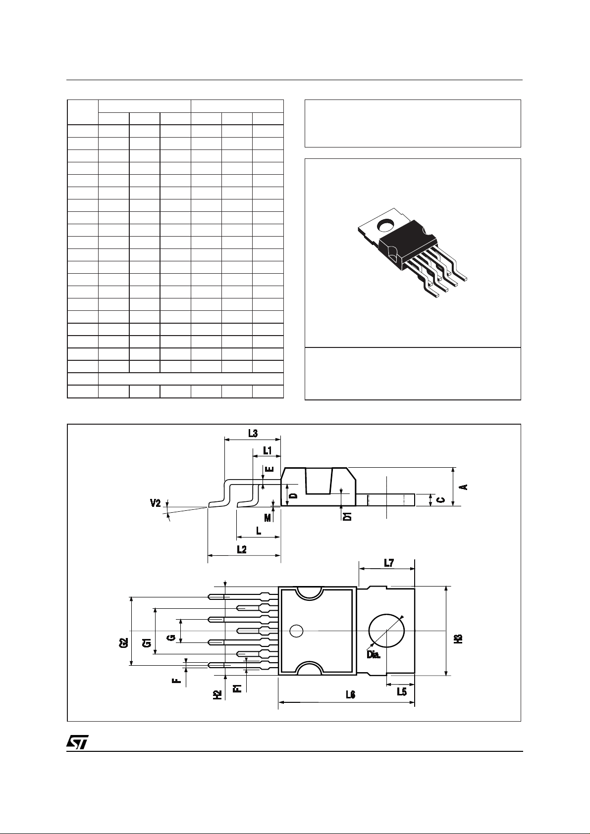
OUTLINE AND
MECHANICAL DATA
Heptawatt (Surface Mount)
April 1999
23/25
Page 24
L3234 - L3235N
DIM.
mm inch
MIN. TYP. MAX. MIN. TYP. MAX.
A 1.60 0.063
A1 0.05 0.15 0.002 0.006
A2 1.35 1.40 1.45 0.053 0.055 0.057
B 0.30 0.37 0.45 0.012 0.014 0.018
C 0.09 0.20 0.004 0.008
D 12.00 0.472
D1 10.00 0.394
D3 8.00 0.315
e 0.80 0.031
E 12.00 0.472
E1 10.00 0.394
E3 8.00 0.315
L 0.45 0.60 0.75 0.018 0.024 0.030
L1 1.00 0.039
K 0°(min.), 3.5˚(typ.), 7°(max.)
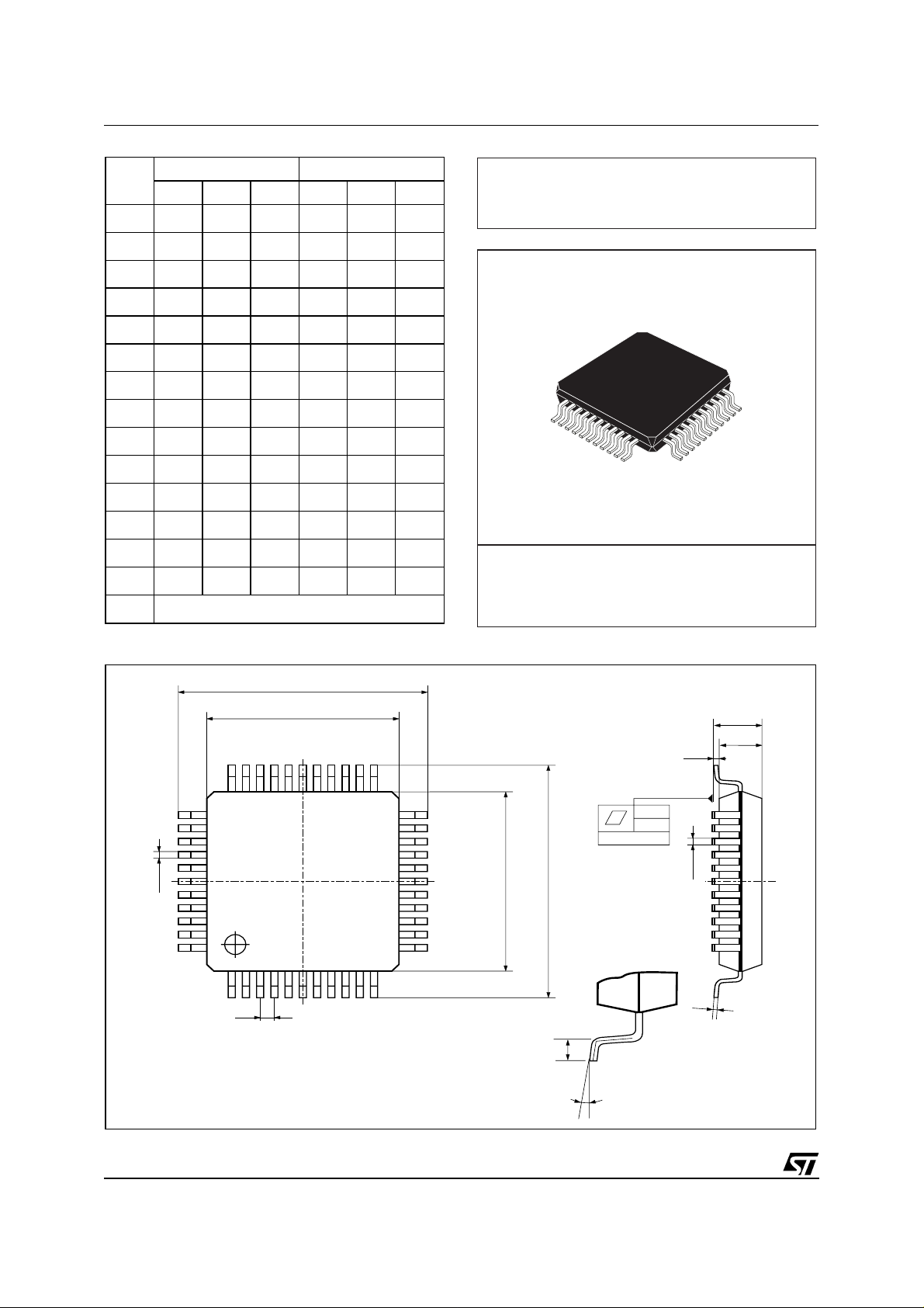
OUTLINE AND
MECHANICAL DATA
TQFP44 (10 x 10)
D
D1
A1
2333
34
B
44
1
e
22
E
E1
12
11
0.10mm
.004
Seating Plane
B
A
A2
C
L
K
TQFP4410
24/25
Page 25

L3234 - L3235N
Information furnishe d is beli eved to be accu rate and reliable. However, STMicroelec tronics assumes no res ponsibility for the consequences
of use of such i nformation nor for any i nfringement of patents or ot her rights of third par ties which may result from its use. No license i s
granted by impli cation or otherwis e under any patent or patent righ ts of STMicroelect ronics. Specifica tion mentioned in this publication are
subject to change without notic e. This public ation supers edes and replaces all information prev iously supplied. STMic roelec tronic s products
are not authorized for use as critical components in life support devices or systems without express written approval of STMicroelectronics.
The ST logo is a registered trademark of STMicroelect roni cs
© 2001 STMicroelectronics – Printed in Italy – All Rights Reserved
STMicroelectronics GROUP OF COMPANIES
Australia - Brazil - Canada - China - Finland - France - Germany - Hong Kong - India - Israel - Italy - Japan - Malaysia - Malta - Morocco -
Singapore - Spain - Sweden - Switzerland - United Kingdom - United States.
http://www.st.com
25/25
 Loading...