

Page 1
L3121B
ApplicationSpecific Discretes
A.S.D.
FEATURES
BIDIRECTIONALFUNCTIONWITH VOLTAGE
PROGRAMMABILITYIN BOTH POSITIVEAND
NEGATIVEPOLARITIES.
PROGRAMMABLE BREAKDOWN VOLTAGE
UP TO100 V.
HOLDINGCURRENT = 150mA min.
HIGHSURGE CURRENTCAPABILITY.
IPP= 100A, 10/1000µs
DESCRIPTION
This device has been especially designed to protect a subscriber line interface circuit (SLIC) with
anintegratedring generator.
Used with the recommended application circuit,
eachline(TIPand RING)is protectedagainstpositive and negative surges. In the positive polarity,
the breakdownvoltage is referenced to the + VB ,
andinthe negativepolarity,the breakdownvoltage
isreferencedto the -Vbat .
TM
PROGRAMMABLE TRANSIENT VOLTAGE
SUPPRESSORFOR SLIC PROTECTION
SIP4
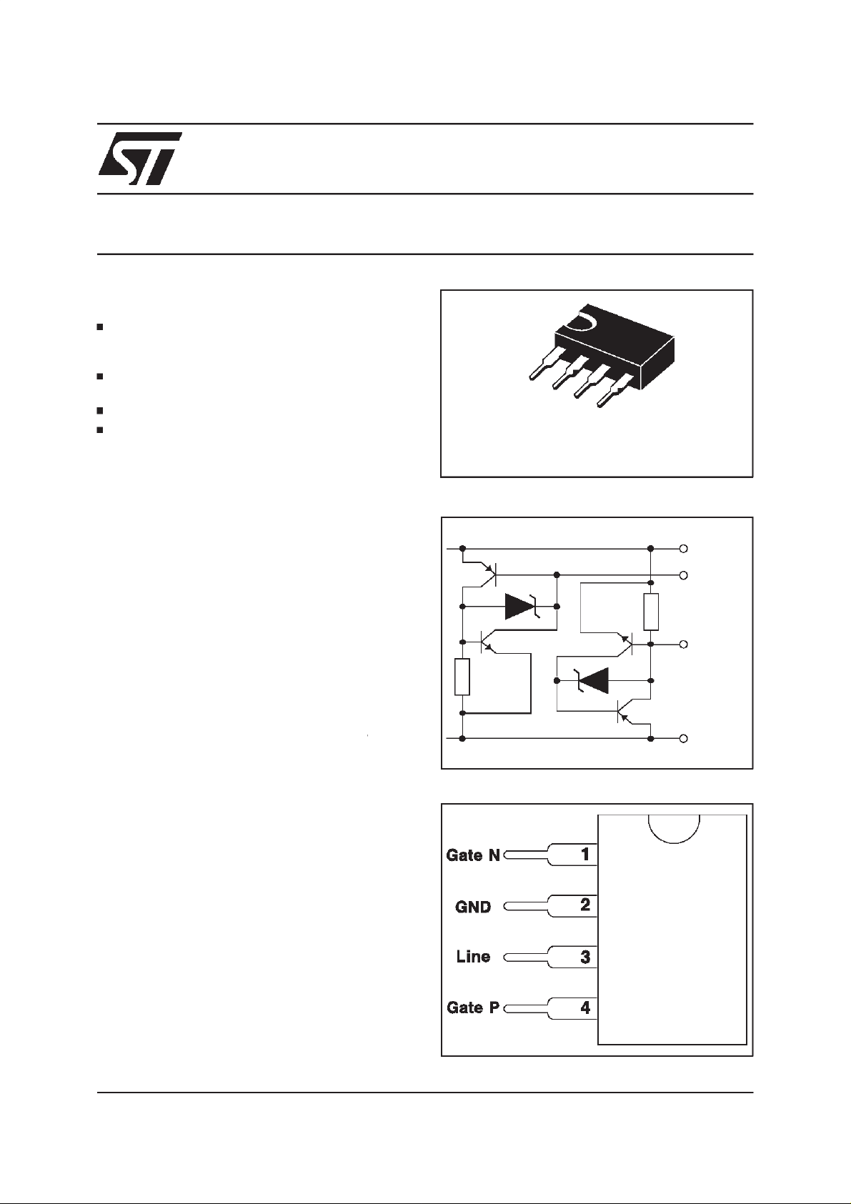
SCHEMATIC DIAGRAM
Line
Gate P
Gate N
Itshigh surgecurrentcapabilitymakesthe L3121B
areliableprotectiondevicefor veryexposedequipment,or when series resistorsare very low.
May 1999 - Ed:4A
GND
CONNECTION DIAGRAM
1/7
Page 2
L3121B
COMPLIESWITHTHE
Peak Surge
FOLLOWING STANDARDS:
ITU-T K20
VDE0433
VDE0878
IEC1000-4-5
FCC Part 68, lightning surge
type A
FCC Part 68, lightning surge
type B
BELLCORE TR-NWT-001089
First level
BELLCORE TR-NWT-001089
Second level
ABSOLUTE MAXIMUM RATINGS
Voltage
(V)
4000 10/700 5/310 100 4000 10/700 5/310 100 4000 1.2/50 1/20 100 -
level4
level4
1500
800
1000 9/720 5/320 25 2500
1000
5000 2/10 2/10 250 10
(Tamb= 25°C)
Voltage
Waveform
(µs)
10/700
1.2/50
10/160
10/560
2/10
10/1000
Current
Waveform
(µs)
5/310
8/20
10/160
10/560
2/10
10/1000
Admissible
Ipp
(A)
100
100
200
100
250
100
Necessary
Resistor
(Ω)
Symbol Parameter Value Unit
I
PP
I
TSM
V
MLG
V
MGL
T
stg
T
j
T
L
Top
Note 1: Variation ofelectrical parameters is given by curves.
Peak pulse current
Non repetitive surge peak on-state
current
Maximum voltage LINE/GND.
Maximum voltage GATE/LINE.
Storage temperature range
Maximum operating junction temperature
Maximum lead temperature for soldering during 10s
Operating temperature range (see note 1)
10/1000µs
2/10µs
100
250
tp = 10 ms 50 A
100
80
- 40 to +150
+ 150
260 °C
-40to+85 °C
-
-
-
-
-
-
A
V
V
°
C
°C
Pulsewaveform10/1000µs
%I
PP
100
50
0
t
r
t
p
THERMAL RESISTANCE
Symbol Parameter Value Unit
Junction-to-ambient
2/7
R
th (j-a)
t
80 °C/W
Page 3

L3121B
ELECTRICALCHARACTERISTICS
Symbol Parameter
V
RM
I
RM
V
BR
V
BO
I
H
I
BO
I
PP
V
GN
I
GN,IGP
C
Stand-off voltage
Reverseleakagecurrent
Breakdown voltage
Breakover voltage
Holding current
Breakover current
Peak pulse current
Gate voltage
Triggeringgate current
Capacitance
1- OPERATIONWITHOUT GATE
I
RM
Type
max. min. max. typ. max. min. max.
(T
@V
amb
RM
=25°C)
VBR@I
R
I
IPP
I
BO
IH
V
BO
@I
BO
I
note1 note 1 note2
VRM
VBO
VBR
H
C
µA V V mA V mA mA mA pF
L3121B
5
8
60
90
2- OPERATIONWITH GATE
@IGN= 200mA IGN@VAC= 60V IGP@VAC= 60V
V
GN
Type
min. max. min. max. max.
V V mA mA mA
L3121B
Note 1 :
See the reference testcircuits for IH,IBOand VBOparameters.
Note 2 :VR= 5 V, F = 1MHz.
0.6 1.8 80 200 180
100 1 180 200 500 150 200
3/7
Page 4

L3121B
REFERENCETEST CIRCUIT FOR IBOand VBOparameters:
tp=20ms
Auto
Transformer
220V/2A
220V
Transformer
220V/800V
5A
TESTPROCEDURE:
PulseTest duration (tp = 20ms):
- For Bidirectionaldevices= SwitchK is closed
- For Unidirectionaldevices= SwitchK isopen.
V
Selection
OUT
- Device with V
-V
- Devicewith V
-V
BO
OUT
BO
OUT
< 200 Volt
= 250V
≥
200 Volt
=480 V
,R1=140 Ω.
RMS
RMS,R2
static
relay.
V
out
= 240 Ω.
K
I,I
BO H
measure
R1
140
R2
240
D.U.T
V
BO
measure
FUNCTIONALHOLDING CURRENT (IH) TEST CIRCUIT= GO- NOGOTEST.
R
D.U.T.
V
= - 48 V
BAT
This isa GO-NOGO Test which allows to confirm the holding current (IH)level in a functionaltest circuit.
This testcan be performed ifthe referencetest circuitcan’t be implemented.
TEST PROCEDURE :
1) Adjust the currentlevel at the IH value by short circuiting the line andGND pinsof the D.U.T.
2) Fire the D.U.T with a surgeCurrent : Ipp = 10A , 10/1000µs.
3) The D.U.T will come back to the OFF-State within a duration of 50 ms max.
-V
P
Surge generator
4/7
Page 5

L3121B
Fig. 1:
Surge peak current versus overload
duration(typicalvalues).
I (A)TSM
40
35
30
25
20
15
10
5
0
1E-2 1E-1 1E+0 1E+1 1E+2 1E+3
Fig. 3:
t(s)
Typical relative variation of breakdown
F=50H z
Tj initial=25°C
voltageversusambient temperature.
V[T]
BR amb
BR amb
V[T =25°C]
2.04
I=1mAR
2.00
Fig. 2:
Typical relative variation of holding current
versusambienttemperature.
H amb
I[T ]
H amb
I[T =25°C]
1.45
1.30
1.15
1.0
0.85
T(°C)amb
0.70
-40 -20 0 20 40 60 80 85
Fig. 4:
Junction capacitance versus reverse
appliedvoltage.
1.06
1.02
0.98
0.94
0.90
Fig.5:
-40 -20 0 20 40 60 80
Typicalrelative variationof leakagecurrent
T(°C)amb
versusambienttemperature.
IR[Tj] / IR [Tj=25°C]
1E+5
1E+4
1E+3
1E+2
1E+1
Tj(°C)
1E+0
25 50 75 100 125
85
Fig. 6:
Typical relative variation of peak pulse
current(10/1000µs) versusambient temperature.
Ipp[Tamb] / Ipp [25°C]
1.10
1.05
1.00
0.95
Tamb(°C)
0.90
-40 -30 -20 -10 0 10 20 30 40 50 60 70 80
5/7
Page 6

L3121B
TypicalSlic ProtectionConcept.
LINE
-Vbat
LINE
R1
GND
R2
G
G
N
N
L3121B
L3121B
G
G
P
P
R3
220nF
220nF
R4
+VB
-Vbat
TIP
SLIC
L3000N
RING
GND
+VB
ORDERCODE
L3121B
DEVICECODE
MARKING : Logo, Date Code, PartNumber
6/7
Page 7

PACKAGEMECHANICAL DATA
SIP4(Plastic)
REF.
L3121B
DIMENSIONS
Millimetres Inches
B
C
Min. Typ. Max. Min. Typ. Max.
A 7.10 0.280
a1 2.80 0.110
I
A
B 10.15 0.400
b1 0.50 0.020
a1
b1
b2
Z
e
L
c1
c2
e3
b2 1.35 1.75 0.053 0.069
C 3.18 3.43 0.125 0.135
c1 0.38 0.50 0.015 0.020
c2 1.30 0.051
e 2.54 0.100
e3 7.62 0.200
I 10.50 0.413
L 3.30 0.130
Z 1.50 0.059
Ordrecode Marking Package Weight Base qty Deliverymode
L3121B SIP4 0.55g
Informationfurnishedis believed to be accurateand reliable.However, STMicroelectronics assumes no responsibility for the consequences of
use of suchinformation nor forany infringement of patents or other rights of thirdparties which may result from its use. No license is grantedby
implicationor otherwise under any patent or patent rights of STMicroelectronics.Specifications mentioned in this publication are subject to
change without notice. This publication supersedes and replaces all informationpreviously supplied.
STMicroelectronicsproducts are not authorized foruse as critical components in life support devices or systems without express written approval of STMicroelectronics.
The ST logo is a registered trademark of STMicroelectronics
1999 STMicroelectronics- Printed in Italy- All rights reserved.
STMicroelectronics GROUP OF COMPANIES
Australia - Brazil - Canada - China - France - Germany - Italy - Japan - Korea - Malaysia - Malta - Mexico - Morocco -
The Netherlands - Singapore - Spain - Sweden - Switzerland - Taiwan - Thailand - United Kingdom - U.S.A.
http://www.st.com
7/7
 Loading...